JP2005168221A - PWM circuit device - Google Patents
PWM circuit device Download PDFInfo
- Publication number
- JP2005168221A JP2005168221A JP2003405280A JP2003405280A JP2005168221A JP 2005168221 A JP2005168221 A JP 2005168221A JP 2003405280 A JP2003405280 A JP 2003405280A JP 2003405280 A JP2003405280 A JP 2003405280A JP 2005168221 A JP2005168221 A JP 2005168221A
- Authority
- JP
- Japan
- Prior art keywords
- output
- output voltage
- circuit
- voltage
- oscillator
- Prior art date
- Legal status (The legal status is an assumption and is not a legal conclusion. Google has not performed a legal analysis and makes no representation as to the accuracy of the status listed.)
- Pending
Links
Images
Landscapes
- Dc-Dc Converters (AREA)
Abstract
Description
本発明は、PWM制御する回路装置に係り、特に、スイッチング電源装置などのコイル負荷を駆動するPWM回路装置に関するものである。 The present invention relates to a circuit device that performs PWM control, and more particularly to a PWM circuit device that drives a coil load such as a switching power supply device.
近年、ディジタル回路技術の進歩により、電源装置をPWM制御することで、装置全体の省電力化が図られるようになってきた。
降圧型スイッチング電源の場合、出力電圧Voutは入力電圧Vinと出力デューティーDを用いると式(1)のように表される。
In recent years, due to the advancement of digital circuit technology, power control of the power supply device has been achieved by the PWM control of the power supply device.
In the case of a step-down switching power supply, the output voltage Vout is expressed as shown in Expression (1) when the input voltage Vin and the output duty D are used.
Vout = D × Vin ‥‥(1)
出力電圧Voutを大きくするには、入力電圧Vinを大きくするか、出力デューティーDを大きくする必要がある。一般に入力電圧Vinが制限されている場合が多いため、出力デューティーDを可能なかぎり大きくする。また、出力デューティーDを大きくすることで、後述するように、過渡応答性の改善が測れる。従って、PWM制御する装置では、一般に出力デューティーを向上させることが目指されている。
Vout = D × Vin (1)
In order to increase the output voltage Vout, it is necessary to increase the input voltage Vin or increase the output duty D. In general, since the input voltage Vin is often limited, the output duty D is increased as much as possible. Further, by increasing the output duty D, the transient response can be improved as will be described later. Therefore, in an apparatus that performs PWM control, it is generally aimed to improve the output duty.
しかし、このような装置では、コイル負荷を駆動するため、PWM制御のデューティーを100%とする(すなわち、DC出力を印加する)と、駆動するコイル負荷が等価的に小さな抵抗値を有する抵抗となる。その結果、大電流が流れ、かかるコイル負荷を破壊してしまう。この問題を防止するため、PWMの最大デューティーを100%としないように制限する方法が一般的に用いられている。 However, in such a device, in order to drive the coil load, when the duty of PWM control is set to 100% (that is, the DC output is applied), the driving coil load is equivalent to a resistor having a small resistance value. Become. As a result, a large current flows and destroys the coil load. In order to prevent this problem, a method of limiting the maximum PWM duty not to be 100% is generally used.
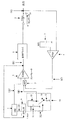
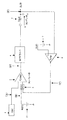
このような従来装置について、以下にその事例を挙げて説明する。図5は従来のPWM回路装置である。
図5において、1は発振器、2はコンパレータ、3は2入力の最小値を出力する最小値回路、4はPWM駆動される出力ドライバ、5はコイル負荷、6はコンデンサ、7は基準電圧源、8は出力電圧(E)と基準電圧源7とを比較してその差を取り出すエラーアンプ、11は基準電圧源である。
Such a conventional apparatus will be described below with examples. FIG. 5 shows a conventional PWM circuit device.
In FIG. 5, 1 is an oscillator, 2 is a comparator, 3 is a minimum value circuit that outputs a minimum value of 2 inputs, 4 is an output driver driven by PWM, 5 is a coil load, 6 is a capacitor, 7 is a reference voltage source,
次に、従来のPWM回路装置の動作について、以下、図5、図6を参照しながら詳しく説明する。
はじめに、図5の各部ごとの動作について説明する。
Next, the operation of the conventional PWM circuit device will be described in detail with reference to FIGS.
First, the operation of each part in FIG. 5 will be described.
エラーアンプ8は基準電圧源7の出力電圧と本回路の出力電圧(E)とを比較し出力(C)とする。ここで基準電圧源7の出力電圧が出力電圧(E)より高いとき、エラーアンプ8の出力電圧は、基準電圧源7の出力電圧と出力電圧(E)との差に比例した分だけ高い出力電圧(C)を出力する。逆に、基準電圧源7の出力電圧が出力電圧(E)より低いとき、エラーアンプ8の出力電圧は、基準電圧源7の出力電圧と出力電圧(E)との差に比例した分だけ低い出力電圧(C)を出力する。
The
最小値回路3は基準電圧源11の出力電圧(B)と前記エラーアンプ8の出力電圧(C)とを比較し、両者のうち低い方の電圧を出力する。後述するが、本最小値回路の入力となる(B)は本回路における最大デューティーを制限するための制限電圧であり、通常動作時には最小値回路3の出力はエラーアンプ8の出力(C)となる。
The minimum value circuit 3 compares the output voltage (B) of the
発振器1は本回路のPWM周波数を決定しており、前記発振器1から作成された三角波(A)をコンパレータ2へと出力する。
コンパレータ2は最小値回路3の出力電圧と前記発振器1によって作成された三角波(A)の電圧を比較し、出力電圧(D)とする。コンパレータ2は、発振器1から作成された三角波(A)の電圧が最小値回路3の出力電圧より低いときに出力ドライバ4をオンする。逆に、発振器1から作成された三角波(A)の電圧が最小値回路3の出力電圧より高いときに出力ドライバ4をオフする。
The
The
出力ドライバ4では、前記コンパレータ2の出力電圧(D)に従い、オン・オフ動作を繰り返す。出力ドライバ4がオンとなる期間には、コイル負荷5を介してコンデンサ6を充電し、出力電圧(E)は徐々に増加していく。逆に、前記出力ドライバ4がオフとなる期間には、コンデンサ6に蓄積された電荷が放電していき、出力電圧(E)は低下する。
The output driver 4 repeats the on / off operation according to the output voltage (D) of the
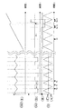
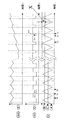
図6(i)(ii)(iii)は従来回路における各部の動作波形のタイミングチャートを示すものであり、横軸を時間tとして以下に示す各部の動作波形を示している。図6(i)にコンパレータ2の入力である発振器1の出力から作成された三角波(A)、最小値回路3の入力となる最大デューティー制限電圧である基準電圧源11の出力電圧(B)、エラーアンプ8の出力電圧(C)を示している。図6(ii)に出力ドライバ4のオン・オフ状態(D)を示している。図6(iii)に出力電圧(E)を示す。
FIGS. 6 (i), (ii), and (iii) are timing charts of the operation waveforms of the respective parts in the conventional circuit, and show the operation waveforms of the following parts with the horizontal axis as time t. FIG. 6 (i) shows a triangular wave (A) created from the output of the
次に、この図6(i)(ii)(iii)のタイミングチャートを用いて、 通常時と電源投入時、あるいは(E)点での負荷電流が急増した時など出力電圧(E)が低下した場合に分けて従来回路の動作説明をする。 Next, using the timing charts of FIGS. 6 (i), (ii), and (iii), the output voltage (E) decreases when the load current at point (E) suddenly increases during normal operation and when the power is turned on. The operation of the conventional circuit will be described separately.
まず通常時の場合について従来回路の動作説明をする。
図6での時間T0からT1のときを考える。
図6(i)において、この区間では、基準電圧源11の出力電圧(B)よりエラーアンプ8の出力電圧(C)が低いので、最小値回路3はエラーアンプ8の出力電圧(C)を出力する。この最小値回路3の出力電圧となる(C)と発振器1から作成された三角波信号(A)とをコンパレータ2で比較する。この区間(時間T0からT1)では、発振器1から作成された三角波(A)が最小値回路3の出力電圧より低いので、コンパレータ2の出力電圧(D)がハイレベルとなることで、出力ドライバ4をオンさせる(図6(ii)参照)。そして、出力ドライバ4がオンとなるので、出力電圧(E)が上昇する(図6(iii)参照)。
First, the operation of the conventional circuit will be described in the normal case.
Consider the time from T0 to T1 in FIG.
In FIG. 6 (i), since the output voltage (C) of the
次に時間T1からT2のときを考える。
この区間でも、基準電圧源11の出力電圧(B)よりエラーアンプ8の出力電圧(C)が低いので、最小値回路3はエラーアンプ8の出力電圧(C)を出力する。この最小値回路3の出力電圧となる(C)と発振器1から作成された三角波信号(A)とをコンパレータ2で比較する。発振器1から作成された三角波(A)が最小値回路3の出力電圧より高くなり、コンパレータ2の出力電圧(D)がローレベルとなることで、出力ドライバ4をオフさせる(図6(ii)参照)。
Next, consider the time from T1 to T2.
Even in this section, since the output voltage (C) of the
そして、出力ドライバ4がオフとなるので、出力電圧(E)が低下する(図6(iii)参照)。以後この動作を繰り返す。
次に電源投入時あるいは、(E)点での負荷電流が急増した時など出力電圧(E)が低下した場合について本従来回路の動作説明をする。
Since the output driver 4 is turned off, the output voltage (E) decreases (see FIG. 6 (iii)). Thereafter, this operation is repeated.
Next, the operation of the conventional circuit will be described in the case where the output voltage (E) is lowered, such as when the power is turned on or when the load current at the point (E) increases rapidly.
図6での時間T3からT4のときを考える。
図6(i)において、この区間では、出力電圧(E)が低いため、基準電圧源7との差が大きく、エラーアンプ8の出力電圧(C)が上昇する。エラーアンプ8の出力電圧(C)が基準電圧源11の出力電圧(B)より高くなり、最小値回路3は基準電圧源11の出力電圧(B)を出力する。前述のように、デューティーはこの最小値回路3の出力電圧から決定されるため、本基準電圧源11の出力電圧(B)が本PWM動作での最大デューティーを決定する制限回路の制限電圧となっている。この区間では、発振器1から作成された三角波(A)が基準電圧源11の出力電圧(B)より低くなり、前述のように、出力ドライバ4をオンさせる(図6(ii)参照)ので、出力電圧(E)が上昇する(図6(iii)。
Consider the time T3 to T4 in FIG.
In FIG. 6 (i), since the output voltage (E) is low in this section, the difference from the
次に時間T4からT5の区間では、発振器1から作成された三角波(A)が基準電圧源11の出力電圧(B)より高くなり(図6(i)参照)、基準電圧(B)によって最大デューティーが制限されるので、この区間では出力ドライバ4をオフさせる(図6(ii)参照)。その結果、出力電圧(E)が下降する(図6(iii)。
Next, in a period from time T4 to T5, the triangular wave (A) generated from the
この従来装置では、デューティーを上げるためには最大デューティーを決定する、基準電圧源11の出力である(B)と発振器1から作成された三角波(A)の最大値(デューティー100%に相当)との差(図6(i)中のXに示す)を小さくすれば良いことになる。しかし、発振器1から作成される三角波(A)のピーク電圧のばらつきが考えられるため、前記Xを十分に小さくできない。
In this conventional device, in order to increase the duty, the maximum duty is determined (B) which is the output of the
このばらつきの原因としては、コンパレータ2での遅延、基準電圧のばらつき、その他回路での遅延などが考えられる。そのため、ばらつきがあっても決してデューティーが100%とならないようにするため、前記Xを大きくする必要がある。
Possible causes of the variation include a delay in the
また、最大デューティーを100%とすることができないため、PWM1周期ごとに前記最大デューティーを制限する電圧(B)と発振器1から作成される三角波(A)で決定される期間にオフとなる。そのため、負荷電流の急増などにより、出力電圧が下がってしまうと、出力ドライバ4がオン・オフを繰り返しながら電圧上昇していく。そのため十分な過渡応答性が得られない、という課題がある。
Further, since the maximum duty cannot be set to 100%, the duty is turned off during a period determined by the voltage (B) that limits the maximum duty and the triangular wave (A) generated from the
本発明は上記欠点を鑑み、ばらつきに対して安定に、最大デューティーを上げ、かつ、急激な入出力の変動への応答性・電流能力を改善したPWM回路装置を提供することを目的とする。 In view of the above-described drawbacks, an object of the present invention is to provide a PWM circuit device in which the maximum duty is stably increased with respect to variations, and the responsiveness / current capability to a sudden input / output fluctuation is improved.
本発明のPWM回路装置は、コイル負荷をPWM駆動して出力電圧を出力するPWM回路装置であって、基準電圧と前記出力電圧を比較するエラーアンプと、前記エラーアンプの出力と他の入力を比較して両者のうち低い方の電圧を出力する最小値回路と、基準周波数を出力する発振器と、前記最小値回路の出力と前記発振器の出力を比較するコンパレータと、前記コンパレータの出力と前記発振器の出力を用いて前記コンパレータの出力を数えるカウンタと、前記カウンタの出力に応じて出力電圧を変える基準電圧源作成回路とを設け、前記基準電圧源作成回路の出力を最小値回路の前記他の入力として印加し、前記コンパレータの出力側の信号で前記コイル負荷を駆動することを特徴とする。 The PWM circuit device of the present invention is a PWM circuit device that outputs an output voltage by PWM driving a coil load, an error amplifier that compares a reference voltage with the output voltage, an output of the error amplifier, and other inputs. A minimum value circuit that outputs the lower voltage of the two in comparison, an oscillator that outputs a reference frequency, a comparator that compares the output of the minimum value circuit with the output of the oscillator, the output of the comparator, and the oscillator A counter that counts the output of the comparator using the output of the comparator, and a reference voltage source creation circuit that changes an output voltage according to the output of the counter, and outputs the reference voltage source creation circuit to the other of the minimum value circuit It is applied as an input, and the coil load is driven by a signal on the output side of the comparator.
本発明は、ばらつきに対して安定に、最大デューティーを上げ、かつ、急激な入出力の変動への応答性・電流能力を改善できる。 The present invention can increase the maximum duty in a stable manner against variations, and improve the responsiveness and current capability against sudden input / output fluctuations.
以下、本発明の実施の形態を図1〜図4に基づいて説明する。
図1に本発明による回路の一例を示す。
1は発振器、2はコンパレータ、3は2入力の最小値を出力する最小値回路、4はPWM駆動される出力ドライバ、5はコイル負荷、6はコンデンサ、7は基準電圧源、8は出力電圧(E)と基準電圧源7とを比較して、その差を取り出すエラーアンプ、9は発振器1の出力パルス(F)の立ち上がりを計測するカウンタ、10はカウンタ9の出力に従い、オン・オフを繰り返すスイッチ、11は基準電圧源、12は前記基準電圧源11と前記スイッチ10の間に接続された抵抗、13は前記スイッチ10とグラウンドとの間に接続された抵抗、14は基準電圧源作成回路である。
Hereinafter, embodiments of the present invention will be described with reference to FIGS.
FIG. 1 shows an example of a circuit according to the present invention.
1 is an oscillator, 2 is a comparator, 3 is a minimum value circuit that outputs a minimum value of 2 inputs, 4 is an output driver driven by PWM, 5 is a coil load, 6 is a capacitor, 7 is a reference voltage source, and 8 is an output voltage (E) is an error amplifier that compares the
次に、本発明によるPWM回路装置の動作について、図1〜図4を参照しながら詳しく説明する。
はじめに、図1の各部ごとの動作について説明する。ただし、既に図5を用いて従来方式のPWM回路装置の動作として説明した部分と共通する部分は省略する。
Next, the operation of the PWM circuit device according to the present invention will be described in detail with reference to FIGS.
First, the operation of each part in FIG. 1 will be described. However, the parts common to those already described as the operation of the conventional PWM circuit device with reference to FIG. 5 are omitted.
図5と異なる要素として、最小値回路3に入力する基準電圧源による制限電圧(B)を作成する回路要素について説明する。
図5に示した従来回路では、基準電圧源11の出力のみで決まる1つの電圧値であるが、本発明によるPWM回路装置では図1に示すようにその値を2つとする。それらはスイッチ10をオフとすることで基準電圧源11の出力電圧を抵抗12を介して出力電圧(B)として出力する値と、スイッチ10をオンとし、基準電圧源11の出力電圧を抵抗12と抵抗13によって分圧した値の2通りである。
As a different element from FIG. 5, a circuit element for creating the limit voltage (B) by the reference voltage source input to the minimum value circuit 3 will be described.
In the conventional circuit shown in FIG. 5, the voltage value is determined only by the output of the
ここで基準電圧源11の出力電圧を抵抗12を介して(B)として出力する場合の電圧値を、発振器1から作成された三角波(A)の最大値よりも高くする。一方、基準電圧源11の出力電圧を抵抗12と抵抗13によって分圧した値は発振器1から作成される三角波(A)の最大値より低くする。
Here, the voltage value when the output voltage of the
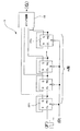
前記スイッチ10をオン・オフ制御するためカウンタ9を用いる。本カウンタの動作について図4を用いて説明する。
このカウンタ9は、D型フリップフロップFF1〜FFnと、各フリップフロップの出力の出力に基づいて設定値になったことを検出するロジック回路15とで構成されている。
A
The
前記カウンタ9は発振器1の出力パルス(F)の立ち上がりを計測する。ただし、このカウンタ9はコンパレータ2の出力(D)がオフであるとき(電圧がローレベルである)はリセットされるため、コンパレータ2の出力(D)がオンであるときにカウンタ9が動作し、設定したあるカウント数(これをn回とする)をカウントした場合にスイッチ10をオンする(出力(G))。すなわち、コンパレータ2の出力が連続して100%デューティーを出した回数を数えて、その回数が設定した値(n回)になると基準電圧源作成回路14の出力を低くして、コンパレータの出力を100%以下の値にする。
The
図2(i)(ii)(iii)は本発明によるPWM回路装置における各部の動作波形のタイミングチャートを示すものであり、横軸を時間tとして以下に示す各部の動作波形を示している。図2(i)にコンパレータ2の入力である発振器1の出力から作成された三角波(A)、最小値回路3の入力となる基準電圧源作成回路14の出力電圧(B)、エラーアンプ8の出力電圧(C)を示している。図2(ii)に出力ドライバ4のオン・オフ状態(D)を示している。図2(iii)に出力電圧(E)を示す。
FIGS. 2 (i), (ii), and (iii) are timing charts of the operation waveforms of the respective parts in the PWM circuit device according to the present invention, and show the operation waveforms of the following parts with the horizontal axis as time t. FIG. 2 (i) shows a triangular wave (A) created from the output of the
図2(i)(ii)及び(iii)に示すタイミングチャートを用いて、通常時と電源投入時あるいは、(E)点での負荷電流が急増した時など出力電圧(E)が低下した場合に分けて動作を説明をする。 When the output voltage (E) decreases using the timing chart shown in FIGS. 2 (i), (ii), and (iii), such as when the power is turned on at normal times and when the load current at point (E) increases rapidly. The operation will be described separately.
まず、通常時の本発明によるPWM回路装置の動作説明をする。
図2(i)での時間T0からT1のときを考える。
カウンタ9は設定した回数までカウント・アップされないので、スイッチ10はオフである。このため、基準電圧源作成回路14の出力電圧(B)は基準電圧源11の出力電圧が抵抗12を介して、最小値回路3へと入力される。基準電圧源作成回路14の出力電圧(B)がエラーアンプ8の出力電圧(C)より高いので、最小値回路3はエラーアンプ8の出力電圧(C)を出力する。この最小値回路3の出力電圧となる(C)と発振器1から作成された三角波信号(A)とをコンパレータ2で比較する。このとき、発振器1から作成された三角波(A)が最小値回路3の出力電圧(C)より低くなり、コンパレータ2の出力電圧(D)がハイレベルとなり出力ドライバ4をオンさせる(図2(ii)参照)。そして、出力ドライバ4がオンするので、出力電圧(E)が上昇する(図2(iii)参照)。
First, the operation of the PWM circuit device according to the present invention during normal operation will be described.
Consider the time from T0 to T1 in FIG.
Since the
次に図2(i)での時間T1からT2のときを考える。
このときでもカウンタ9は設定した回数までカウント・アップされず、スイッチ10はオフであり、基準電圧源作成回路14の出力電圧(B)は基準電圧源11の出力電圧が抵抗12を介して現われる。このとき、基準電圧源作成回路14の出力電圧(B)がエラーアンプ8の出力電圧(C)より高いので、最小値回路3はエラーアンプ出力電圧(C)を出力する。発振器1から作成された三角波(A)が最小値回路3の出力電圧より高くなり、コンパレータ2の出力電圧(D)がローレベルとなり、出力ドライバ4をオフさせる(図2(ii)参照)。そして、出力ドライバ4がオフとなるので、出力電圧(E)が低下する(図2(iii)参照)。
Next, consider the time T1 to T2 in FIG.
Even at this time, the
次に電源投入時あるいは、(E)点での負荷電流が急増した時など出力電圧(E)が低下した場合の動作説明をする。
図2(i)での時間T3からT4のときを考える。
Next, an operation will be described when the output voltage (E) decreases, such as when the power is turned on or when the load current at point (E) suddenly increases.
Consider the time T3 to T4 in FIG.
このとき、エラーアンプ8の出力は最大値まで上昇している。一方、カウンタ9はカウント・アップを続けているが、この区間では、カウンタ9のカウント値が予め設定したカウント回数にまで達しておらず、スイッチ10はオフのままで基準電圧源作成回路14の出力電圧(B)は基準電圧源11の出力が抵抗12を介して出力される。エラーアンプ8の出力電圧(C)が基準電圧源作成回路14の出力電圧(B)より小さいので、最小値回路3はエラーアンプ8の出力電圧(C)を出力する。時間T3からT4の期間では発振器1から作成された三角波(A)がエラーアンプ8の出力電圧(C)より小さい。前述のように、この区間では出力ドライバ4をオンさせる(図2(ii)参照)ので、出力電圧(E)が上昇する(図2(iii)参照)。
At this time, the output of the
次に時間T4になったときに、前記カウンタ9がカウント・アップし、所望の特性を満たすように予め設定した回数に到達したとする。このとき、スイッチ10がオンとなり、基準電圧源作成回路14の出力電圧(B)は基準電圧源11の出力を抵抗12及び抵抗13にて分圧した電圧となる。このとき、エラーアンプ8の出力電圧(C)が基準電圧源作成回路14の出力電圧(B)より大きくなる。よって時間T5になり、発振器1から作成された三角波(A)が最小値出力回路の出力電圧(C)より大きくなり(図2(i)参照)、出力ドライバ4をオフさせる(図2(ii)参照)ので、出力電圧(E)が下降する(図2(iii)参照)。
Next, it is assumed that when the time T4 comes, the
次に時間T6になり、発振器1から作成された三角波(A)が最小値回路の出力電圧より小さくなり(図2(i)参照)、再び、出力ドライバ4をオンさせ(図2(ii)参照)、コイル負荷5を介してコンデンサ6を充電し、出力電圧(E)が上昇する(図2(iii)参照)。時間T7となり、出力ドライバ4の入力(D)がオフとなり(図2(ii)参照)、再び、カウンタ9がリセットされて、スイッチ10がオフとなり、基準電圧源作成回路14の出力電圧(B)が基準電圧源11の出力を抵抗12を介して出力した値となる(図2(i)参照)。ここから再び、カウンタ9がカウント・アップする。
Next, at time T6, the triangular wave (A) generated from the
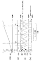
図3を用いてカウンタのカウント回数と抵抗12および抵抗13の値によってスイッチ10がオンとなったときに(B)に出力される電圧を設定することで、任意のデューティーを実現する原理について説明する。
The principle of realizing an arbitrary duty by setting the voltage output to (B) when the
図3に示すように発振器1の出力パルスの立ち上がりをn回カウンタ9がカウントするごとに、スイッチ10を一度オンさせる。このとき、抵抗12および抵抗13によって決定したこのときのデューティーをm[%]とする、このときのデューティーDは次式(2)にて表現される。
As shown in FIG. 3, every time the
D = 100[%] × (n−1)/n + m[%] × 1/n ‥‥(2)
上記の式(2)の変数、m,nを任意に決定することで、デューティーを調整することが出来る。
D = 100 [%] × (n−1) / n + m [%] × 1 / n (2)
The duty can be adjusted by arbitrarily determining the variables m and n in the above equation (2).
このように、カウンタ9のカウント回数と基準電圧源作成回路14の出力である、抵抗12および抵抗13の値によってスイッチ10がオンとなったときに(B)に出力される電圧を任意に調整することで、電源投入時あるいは、(E)点での負荷電流が急増した時など出力電圧(E)が低下した場合において、従来方式と比較して、必ず1周期に一度の休止期間を含まないため、出力電圧が早く所望の値となり、かつ抵抗12及び抵抗13の値を決定することで自由に式(2)中のmを決定することができ、また、この値を比較的大きくすることができ、かつ、デューティーが必ず100%とはならない、所望の最大デューティー制御のPWM回路装置を実現できる。
Thus, the voltage output to (B) when the
本発明は、コイル負荷をPWM駆動するスイッチング電源装置などの性能が向上し、この電源装置を使用した各種電気機器の安定した動作に寄与できる。 The present invention improves the performance of a switching power supply device that performs PWM driving of a coil load, and can contribute to stable operation of various electric devices using the power supply device.
1 発振器
2 コンパレータ
3 最小値回路
4 出力ドライバ
5 コイル負荷
6 コンデンサ
7 基準電圧源
8 エラーアンプ
9 カウンタ
10 スイッチ
11 基準電圧源
12 抵抗
13 抵抗
14 基準電圧源作成回路
(A) 発振器1から作成した三角波
(B) 基準電圧源2の出力あるいは、スイッチ10を介して抵抗12および13にて分割された出力
(C) エラーアンプ8の出力
(D) コンパレータ2の出力
(E) 出力電圧
(F) 発振器1の出力パルス
(G) カウンタ9の出力
DESCRIPTION OF
Claims (1)
基準電圧と前記出力電圧を比較するエラーアンプと、
前記エラーアンプの出力と他の入力を比較して両者のうち低い方の電圧を出力する最小値回路と、
基準周波数を出力する発振器と、
前記最小値回路の出力と前記発振器の出力を比較するコンパレータと、
前記コンパレータの出力と前記発振器の出力を用いて前記コンパレータの出力を数えるカウンタと、
前記カウンタの出力に応じて出力電圧を変える基準電圧源作成回路と
を設け、前記基準電圧源作成回路の出力を最小値回路の前記他の入力として印加し、前記コンパレータの出力側の信号で前記コイル負荷を駆動する
PWM回路装置。 A PWM circuit device that PWM drives a coil load and outputs an output voltage,
An error amplifier for comparing a reference voltage and the output voltage;
A minimum value circuit that compares the output of the error amplifier with other inputs and outputs the lower voltage of both, and
An oscillator that outputs a reference frequency;
A comparator that compares the output of the minimum value circuit with the output of the oscillator;
A counter that counts the output of the comparator using the output of the comparator and the output of the oscillator;
A reference voltage source creating circuit that changes an output voltage according to the output of the counter, and applying the output of the reference voltage source creating circuit as the other input of the minimum value circuit, and the signal on the output side of the comparator PWM circuit device that drives a coil load.
Priority Applications (1)
| Application Number | Priority Date | Filing Date | Title |
|---|---|---|---|
| JP2003405280A JP2005168221A (en) | 2003-12-04 | 2003-12-04 | PWM circuit device |
Applications Claiming Priority (1)
| Application Number | Priority Date | Filing Date | Title |
|---|---|---|---|
| JP2003405280A JP2005168221A (en) | 2003-12-04 | 2003-12-04 | PWM circuit device |
Publications (1)
| Publication Number | Publication Date |
|---|---|
| JP2005168221A true JP2005168221A (en) | 2005-06-23 |
Family
ID=34727993
Family Applications (1)
| Application Number | Title | Priority Date | Filing Date |
|---|---|---|---|
| JP2003405280A Pending JP2005168221A (en) | 2003-12-04 | 2003-12-04 | PWM circuit device |
Country Status (1)
| Country | Link |
|---|---|
| JP (1) | JP2005168221A (en) |
Cited By (4)
| Publication number | Priority date | Publication date | Assignee | Title |
|---|---|---|---|---|
| CN102902295A (en) * | 2011-03-11 | 2013-01-30 | 英飞凌科技奥地利有限公司 | Methods and apparatus for voltage regulation with dynamic transient optimization |
| JP2016511629A (en) * | 2013-03-14 | 2016-04-14 | クゥアルコム・インコーポレイテッドQualcomm Incorporated | System and method for 100 percent duty cycle in a switching regulator |
| CN111766912A (en) * | 2020-06-30 | 2020-10-13 | 启攀微电子(上海)有限公司 | Control circuit of wide-voltage low-power-consumption voltage-stabilizing source |
| CN113114172A (en) * | 2021-04-30 | 2021-07-13 | 科世达(上海)机电有限公司 | Circuit and device for controlling duty ratio of PWM signal |
-
2003
- 2003-12-04 JP JP2003405280A patent/JP2005168221A/en active Pending
Cited By (4)
| Publication number | Priority date | Publication date | Assignee | Title |
|---|---|---|---|---|
| CN102902295A (en) * | 2011-03-11 | 2013-01-30 | 英飞凌科技奥地利有限公司 | Methods and apparatus for voltage regulation with dynamic transient optimization |
| JP2016511629A (en) * | 2013-03-14 | 2016-04-14 | クゥアルコム・インコーポレイテッドQualcomm Incorporated | System and method for 100 percent duty cycle in a switching regulator |
| CN111766912A (en) * | 2020-06-30 | 2020-10-13 | 启攀微电子(上海)有限公司 | Control circuit of wide-voltage low-power-consumption voltage-stabilizing source |
| CN113114172A (en) * | 2021-04-30 | 2021-07-13 | 科世达(上海)机电有限公司 | Circuit and device for controlling duty ratio of PWM signal |
Similar Documents
| Publication | Publication Date | Title |
|---|---|---|
| JP4631916B2 (en) | Boost DC-DC converter | |
| CN105075088B (en) | System and method for realizing 100% duty ratio in switching regulator modulator | |
| JP5577829B2 (en) | Power supply device, control circuit, and control method for power supply device | |
| CN105356746B (en) | Turn-on time generation circuit and supply convertor for supply convertor | |
| CN103066823B (en) | Controller and control method of switch power source | |
| JP2006006004A (en) | Buck-boost DC-DC converter | |
| JP5479940B2 (en) | Buck-boost DC-DC converter and vehicular lamp | |
| JP6101463B2 (en) | Controller for DC / DC converter | |
| KR20070108088A (en) | Switching voltage regulators and control signal generation method | |
| US20040257056A1 (en) | Switching regulator with improved load transient efficiency and method thereof | |
| JP5708202B2 (en) | DC-DC converter control method and DC-DC converter control circuit | |
| JP2003244944A (en) | DC-DC converter, electronic equipment, duty ratio setting circuit | |
| JP5456495B2 (en) | Buck-boost switching power supply control circuit, buck-boost switching power supply, and buck-boost switching power supply control method | |
| JP2008067505A (en) | Switching power supply and control method in the same | |
| JP4487649B2 (en) | Control device for step-up / step-down DC-DC converter | |
| JP2006014559A (en) | Dc/dc converter | |
| CN108880237B (en) | Switching time generating circuit and switching time control method of switching converter | |
| JP3892333B2 (en) | PFM control switching regulator control circuit | |
| JP5630895B2 (en) | Switching power supply circuit | |
| JP6457242B2 (en) | Switching power supply | |
| TWI654823B (en) | Voltage conversion device | |
| JP2005168221A (en) | PWM circuit device | |
| US20140375285A1 (en) | Dc-dc boost converter | |
| JP4438507B2 (en) | Current mode step-down switching regulator | |
| JP2010063231A (en) | Switching regulator |