JP2005191202A - 半導体装置 - Google Patents
半導体装置 Download PDFInfo
- Publication number
- JP2005191202A JP2005191202A JP2003429403A JP2003429403A JP2005191202A JP 2005191202 A JP2005191202 A JP 2005191202A JP 2003429403 A JP2003429403 A JP 2003429403A JP 2003429403 A JP2003429403 A JP 2003429403A JP 2005191202 A JP2005191202 A JP 2005191202A
- Authority
- JP
- Japan
- Prior art keywords
- region
- insulating layer
- semiconductor device
- layer
- channel stopper
- Prior art date
- Legal status (The legal status is an assumption and is not a legal conclusion. Google has not performed a legal analysis and makes no representation as to the accuracy of the status listed.)
- Pending
Links
Images


Classifications
-
- H—ELECTRICITY
- H10—SEMICONDUCTOR DEVICES; ELECTRIC SOLID-STATE DEVICES NOT OTHERWISE PROVIDED FOR
- H10D—INORGANIC ELECTRIC SEMICONDUCTOR DEVICES
- H10D30/00—Field-effect transistors [FET]
- H10D30/01—Manufacture or treatment
- H10D30/021—Manufacture or treatment of FETs having insulated gates [IGFET]
- H10D30/027—Manufacture or treatment of FETs having insulated gates [IGFET] of lateral single-gate IGFETs
-
- H—ELECTRICITY
- H10—SEMICONDUCTOR DEVICES; ELECTRIC SOLID-STATE DEVICES NOT OTHERWISE PROVIDED FOR
- H10D—INORGANIC ELECTRIC SEMICONDUCTOR DEVICES
- H10D62/00—Semiconductor bodies, or regions thereof, of devices having potential barriers
- H10D62/10—Shapes, relative sizes or dispositions of the regions of the semiconductor bodies; Shapes of the semiconductor bodies
- H10D62/113—Isolations within a component, i.e. internal isolations
- H10D62/115—Dielectric isolations, e.g. air gaps
-
- H—ELECTRICITY
- H10—SEMICONDUCTOR DEVICES; ELECTRIC SOLID-STATE DEVICES NOT OTHERWISE PROVIDED FOR
- H10D—INORGANIC ELECTRIC SEMICONDUCTOR DEVICES
- H10D62/00—Semiconductor bodies, or regions thereof, of devices having potential barriers
- H10D62/10—Shapes, relative sizes or dispositions of the regions of the semiconductor bodies; Shapes of the semiconductor bodies
- H10D62/17—Semiconductor regions connected to electrodes not carrying current to be rectified, amplified or switched, e.g. channel regions
- H10D62/213—Channel regions of field-effect devices
- H10D62/221—Channel regions of field-effect devices of FETs
- H10D62/235—Channel regions of field-effect devices of FETs of IGFETs
Landscapes
- Insulated Gate Type Field-Effect Transistor (AREA)
- Element Separation (AREA)
- Metal-Oxide And Bipolar Metal-Oxide Semiconductor Integrated Circuits (AREA)
Abstract
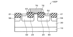
【解決手段】 本発明の半導体装置は、半導体層10の上に設けられたゲート絶縁層60と、
ソース領域およびドレイン領域52と、
前記ソース領域およびドレイン領域52と比して不純物濃度の低い不純物層からなり、該ソース領域およびドレイン領域52を囲むオフセット領域50と、
前記オフセット領域50の外側に設けられたチャネルストッパ領域54と、を有し、
前記チャネルストッパ領域54は、前記ゲート絶縁層60と該チャネルストッパ領域54との距離が前記オフセット領域50と該チャネルストッパ領域54との距離と比して狭くなるように、ゲート絶縁層60の長手方向に突出部を有する。
【選択図】 図2
Description
前記半導体層に設けられたソース領域およびドレイン領域と、
前記ソース領域およびドレイン領域と比して不純物濃度の低い不純物層からなり、該ソース領域およびドレイン領域を囲むオフセット領域と、
前記オフセット領域の外側に設けられたチャネルストッパ領域と、を含み、
前記チャネルストッパ領域は、前記ゲート絶縁層の長手方向における、該ゲート絶縁層と該チャネルストッパ領域との距離が、前記オフセット領域の長手方向における、該オフセット領域と該チャネルストッパ領域との距離と比して狭くなるように突出部を有する。
次に、本実施の形態の半導体装置の製造方法について、図3〜9を参照しながら説明する。図3〜9は、本実施の形態の半導体装置の製造方法の工程を模式的に示す断面図である。
Claims (3)
- 半導体層の上に設けられたゲート絶縁層と、
前記半導体層に設けられたソース領域およびドレイン領域と、
前記ソース領域およびドレイン領域と比して不純物濃度の低い不純物層からなり、該ソース領域およびドレイン領域を囲むオフセット領域と、
前記オフセット領域の外側に設けられたチャネルストッパ領域と、を含み、
前記チャネルストッパ領域は、前記ゲート絶縁層の長手方向における、該ゲート絶縁層と該チャネルストッパ領域との距離が、前記オフセット領域の長手方向における、該オフセット領域と該チャネルストッパ領域との距離と比して狭くなるように突出部を有する、半導体装置。 - 請求項1において、
前記突出部は、前記ゲート絶縁層の略長手方向に突出している、半導体装置。 - 請求項1又は2において、
前記ゲート絶縁層が形成される領域の長手方向の長さと、前記ソース領域およびドレイン領域の長手方向の長さとは略同一である、半導体装置。
Priority Applications (2)
| Application Number | Priority Date | Filing Date | Title |
|---|---|---|---|
| JP2003429403A JP2005191202A (ja) | 2003-12-25 | 2003-12-25 | 半導体装置 |
| US11/022,068 US20050139869A1 (en) | 2003-12-25 | 2004-12-23 | Semiconductor device |
Applications Claiming Priority (1)
| Application Number | Priority Date | Filing Date | Title |
|---|---|---|---|
| JP2003429403A JP2005191202A (ja) | 2003-12-25 | 2003-12-25 | 半導体装置 |
Publications (1)
| Publication Number | Publication Date |
|---|---|
| JP2005191202A true JP2005191202A (ja) | 2005-07-14 |
Family
ID=34697559
Family Applications (1)
| Application Number | Title | Priority Date | Filing Date |
|---|---|---|---|
| JP2003429403A Pending JP2005191202A (ja) | 2003-12-25 | 2003-12-25 | 半導体装置 |
Country Status (2)
| Country | Link |
|---|---|
| US (1) | US20050139869A1 (ja) |
| JP (1) | JP2005191202A (ja) |
Cited By (3)
| Publication number | Priority date | Publication date | Assignee | Title |
|---|---|---|---|---|
| JP2008016820A (ja) * | 2006-06-30 | 2008-01-24 | Taiwan Semiconductor Manufacturing Co Ltd | 半導体構造 |
| JP2014049487A (ja) * | 2012-08-29 | 2014-03-17 | Lapis Semiconductor Co Ltd | 半導体装置及びその製造方法 |
| WO2021112047A1 (ja) * | 2019-12-06 | 2021-06-10 | ローム株式会社 | 半導体装置 |
Families Citing this family (2)
| Publication number | Priority date | Publication date | Assignee | Title |
|---|---|---|---|---|
| DE102005054672B4 (de) * | 2005-11-16 | 2014-06-12 | Austriamicrosystems Ag | Hochvolt-Transistor mit niedriger Threshold-Spannung und einen solchen Hochvolt-Transistor umfassendes Bauelement |
| KR100840787B1 (ko) * | 2007-02-23 | 2008-06-23 | 삼성전자주식회사 | 반도체 장치 및 반도체 장치의 제조 방법 |
Family Cites Families (2)
| Publication number | Priority date | Publication date | Assignee | Title |
|---|---|---|---|---|
| JP2800702B2 (ja) * | 1994-10-31 | 1998-09-21 | 日本電気株式会社 | 半導体装置 |
| JP4686829B2 (ja) * | 1999-09-17 | 2011-05-25 | ソニー株式会社 | 半導体装置および半導体装置の製造方法 |
-
2003
- 2003-12-25 JP JP2003429403A patent/JP2005191202A/ja active Pending
-
2004
- 2004-12-23 US US11/022,068 patent/US20050139869A1/en not_active Abandoned
Cited By (5)
| Publication number | Priority date | Publication date | Assignee | Title |
|---|---|---|---|---|
| JP2008016820A (ja) * | 2006-06-30 | 2008-01-24 | Taiwan Semiconductor Manufacturing Co Ltd | 半導体構造 |
| JP2014049487A (ja) * | 2012-08-29 | 2014-03-17 | Lapis Semiconductor Co Ltd | 半導体装置及びその製造方法 |
| WO2021112047A1 (ja) * | 2019-12-06 | 2021-06-10 | ローム株式会社 | 半導体装置 |
| JPWO2021112047A1 (ja) * | 2019-12-06 | 2021-06-10 | ||
| CN114788015A (zh) * | 2019-12-06 | 2022-07-22 | 罗姆股份有限公司 | 半导体装置 |
Also Published As
| Publication number | Publication date |
|---|---|
| US20050139869A1 (en) | 2005-06-30 |
Similar Documents
| Publication | Publication Date | Title |
|---|---|---|
| JP5816560B2 (ja) | 半導体装置およびその製造方法 | |
| US8022439B2 (en) | Semiconductor device comprising gate electrode surrounding entire circumference of channel region and method for manufacturing the same | |
| JP4971593B2 (ja) | 半導体装置の製造方法 | |
| US20070181950A1 (en) | Semiconductor device and its manufacturing method capable of suppressing junction leakage current | |
| JP4138601B2 (ja) | 半導体装置の製造方法 | |
| JP2006278633A (ja) | 半導体装置の製造方法 | |
| JP2006253397A (ja) | 半導体装置及びその製造方法 | |
| US7531880B2 (en) | Semiconductor device and manufacturing method thereof | |
| JP4471815B2 (ja) | 半導体装置およびその製造方法 | |
| JP2006261161A (ja) | 半導体装置の製造方法 | |
| JP2005191202A (ja) | 半導体装置 | |
| KR20090064658A (ko) | 반도체 소자 및 이의 제조방법 | |
| JP4172796B2 (ja) | 半導体装置の製造方法 | |
| KR102882194B1 (ko) | 고전압 소자, 고전압 소자를 포함하는 반도체 소자 및 반도체 소자를 제조하는 방법 | |
| JP4784738B2 (ja) | 半導体装置 | |
| JP4989074B2 (ja) | 半導体装置 | |
| JP2007073759A (ja) | 半導体装置の製造方法 | |
| KR100595857B1 (ko) | 다공 영역을 이용한 반도체 소자 형성 방법 | |
| JP2003273351A (ja) | 半導体装置およびその製造方法 | |
| JP2007115997A (ja) | 半導体装置 | |
| JP2007115998A (ja) | 半導体装置 | |
| JP2006190743A (ja) | 半導体装置の製造方法 | |
| JP4930725B2 (ja) | 半導体装置 | |
| JP2020181933A (ja) | 半導体装置およびその製造方法 | |
| JP2013247140A (ja) | 半導体装置およびその製造方法 |
Legal Events
| Date | Code | Title | Description |
|---|---|---|---|
| RD04 | Notification of resignation of power of attorney |
Free format text: JAPANESE INTERMEDIATE CODE: A7424 Effective date: 20051221 |
|
| A977 | Report on retrieval |
Free format text: JAPANESE INTERMEDIATE CODE: A971007 Effective date: 20061002 |
|
| A131 | Notification of reasons for refusal |
Free format text: JAPANESE INTERMEDIATE CODE: A131 Effective date: 20080206 |
|
| A521 | Request for written amendment filed |
Free format text: JAPANESE INTERMEDIATE CODE: A523 Effective date: 20080403 |
|
| A02 | Decision of refusal |
Free format text: JAPANESE INTERMEDIATE CODE: A02 Effective date: 20090304 |