JP2005225741A - Apparatus for manufacturing single crystal - Google Patents
Apparatus for manufacturing single crystal Download PDFInfo
- Publication number
- JP2005225741A JP2005225741A JP2004038808A JP2004038808A JP2005225741A JP 2005225741 A JP2005225741 A JP 2005225741A JP 2004038808 A JP2004038808 A JP 2004038808A JP 2004038808 A JP2004038808 A JP 2004038808A JP 2005225741 A JP2005225741 A JP 2005225741A
- Authority
- JP
- Japan
- Prior art keywords
- wire
- single crystal
- sensor
- abnormality
- winch
- Prior art date
- Legal status (The legal status is an assumption and is not a legal conclusion. Google has not performed a legal analysis and makes no representation as to the accuracy of the status listed.)
- Granted
Links
- 239000013078 crystal Substances 0.000 title claims abstract description 53
- 238000004519 manufacturing process Methods 0.000 title claims abstract description 31
- 230000005856 abnormality Effects 0.000 claims abstract description 44
- 238000001514 detection method Methods 0.000 claims description 42
- 230000005540 biological transmission Effects 0.000 claims description 8
- 239000002994 raw material Substances 0.000 claims description 7
- 238000004804 winding Methods 0.000 claims description 2
- 230000001066 destructive effect Effects 0.000 abstract description 3
- 238000007689 inspection Methods 0.000 description 27
- 238000012544 monitoring process Methods 0.000 description 17
- 230000008859 change Effects 0.000 description 9
- 238000000034 method Methods 0.000 description 9
- 230000004907 flux Effects 0.000 description 7
- XUIMIQQOPSSXEZ-UHFFFAOYSA-N Silicon Chemical compound [Si] XUIMIQQOPSSXEZ-UHFFFAOYSA-N 0.000 description 5
- 229910052751 metal Inorganic materials 0.000 description 5
- 239000002184 metal Substances 0.000 description 5
- 230000008054 signal transmission Effects 0.000 description 5
- 229910052710 silicon Inorganic materials 0.000 description 5
- 239000010703 silicon Substances 0.000 description 5
- 238000010586 diagram Methods 0.000 description 3
- 230000008569 process Effects 0.000 description 3
- 239000010453 quartz Substances 0.000 description 3
- VYPSYNLAJGMNEJ-UHFFFAOYSA-N silicon dioxide Inorganic materials O=[Si]=O VYPSYNLAJGMNEJ-UHFFFAOYSA-N 0.000 description 3
- 230000002159 abnormal effect Effects 0.000 description 2
- 238000005452 bending Methods 0.000 description 2
- 238000011109 contamination Methods 0.000 description 2
- 230000007547 defect Effects 0.000 description 2
- 230000005284 excitation Effects 0.000 description 2
- WFKWXMTUELFFGS-UHFFFAOYSA-N tungsten Chemical compound [W] WFKWXMTUELFFGS-UHFFFAOYSA-N 0.000 description 2
- 230000001174 ascending effect Effects 0.000 description 1
- 230000007423 decrease Effects 0.000 description 1
- 230000000694 effects Effects 0.000 description 1
- 239000011261 inert gas Substances 0.000 description 1
- 238000012986 modification Methods 0.000 description 1
- 230000004048 modification Effects 0.000 description 1
- 230000003287 optical effect Effects 0.000 description 1
- 230000002093 peripheral effect Effects 0.000 description 1
- 230000009467 reduction Effects 0.000 description 1
- 239000004065 semiconductor Substances 0.000 description 1
- 229910001220 stainless steel Inorganic materials 0.000 description 1
- 235000012431 wafers Nutrition 0.000 description 1
Images
Landscapes
- Crystals, And After-Treatments Of Crystals (AREA)
Abstract
Description
本発明は、石英るつぼ等に収容された原料融液から種結晶を用いて単結晶インゴットを成長させながらワイヤで引き上げる単結晶製造装置に関する。 The present invention relates to a single crystal manufacturing apparatus for pulling up with a wire while growing a single crystal ingot using a seed crystal from a raw material melt contained in a quartz crucible or the like.
半導体ウエーハの製造に使用される高純度の単結晶インゴットは、一般に、石英るつぼのシリコン融液から種結晶を核として成長させつつワイヤで引き上げるチョコラルスキー法(CZ法)で製造され、そのための各種の製造装置(例えば、特許文献1参照)が知られている。このCZ法による単結晶製造装置の一例を図5に示す。 High-purity single crystal ingots used in the manufacture of semiconductor wafers are generally manufactured by the Choralsky method (CZ method) in which a seed crystal is grown as a nucleus from a silicon melt of a quartz crucible and pulled up with a wire. (See, for example, Patent Document 1). An example of an apparatus for producing a single crystal by this CZ method is shown in FIG.
図5の装置は、縦長の気密チャンバー1の上端に回転ボックス10を連接したもので、チャンバー1の下部に石英製るつぼ2が回転及び上下動可能に配置され、るつぼ2の周りにヒーター3が設置される。回転ボックス10内にはウインチ11が設置され、ウインチ11に巻回されたワイヤ12が回転ボックス10の底部を貫通してチャンバー1内に吊り下がる。ワイヤ12は、ステンレス線やタングステン線などの金属素線から成る高耐熱性の撚り線で、チャンバー1内に吊り下がるワイヤ12の下端部にチャック13を固定している。回転ボックス10はチャンバー1上に水平方向に回転可能に連接され、ウインチ11をワイヤ繰出し方向に正回転させるとワイヤ12がチャック13を吊り下げた状態でチャンバー1内を下降し、ウインチ11を逆回転させるとワイヤ12がウインチ11に巻き取られてチャンバー1内をチャック13と共に上昇する。
The apparatus shown in FIG. 5 has a
図5の単結晶製造装置は以下のように作動する。まずウインチ11でワイヤ12を巻き上げ、チャック13の下端に種結晶を取付ける。チャンバー1内を真空又は不活性ガス雰囲気にし、ヒーター3でるつぼ2内のシリコン単結晶又は多結晶の原料を加熱溶融させる。ウインチ11を正回転させてワイヤ12を繰り出し、チャック13をるつぼ2内のシリコン融液4に向けて下降させる。チャック13下端の種結晶をシリコン融液4の表面に接触させて種結晶の周りに単結晶を成長させ、ウインチ11を低速で逆回転させてワイヤ12でチャック13を引き上げる。この引き上げでシリコン融液4から所望の直径の単結晶インゴット5が成長しながらワイヤ12で引き上げられる。単結晶インゴット5が所定の長さに成長し、チャンバー1内の上部まで引き上げられると、ウインチ11が回転停止して結晶インゴット5の取出作業が行われる。
上記チャンバー内におけるワイヤは、1600℃超の高温融液に晒されるだけでなく、引き上げインゴット重量の増大(大径化、長尺化)に伴いその使用条件はますます過酷になっている。さらに、ワイヤは、単結晶インゴットを引き上げながら捩れ、ウインチに屈曲しながら巻き取られる動作を繰り返すために、金属疲労が進行しやすい使用条件下にある。このため、現在の単結晶製造現場においては、ワイヤを早い時期に定期的に新品と交換するようにして、使用時のワイヤ損傷、最悪の場合のワイヤ断線によるトラブル発生を回避するようにしている。 The wire in the chamber is not only exposed to a high-temperature melt exceeding 1600 ° C., but the use conditions are becoming more severe as the weight of the pulled ingot increases (larger diameter, longer length). In addition, the wire is twisted while pulling up the single crystal ingot and is repeatedly wound up while being bent into the winch, so that the metal fatigue is likely to progress. For this reason, at the current single crystal manufacturing site, the wires are regularly replaced with new ones at an early stage so as to avoid the occurrence of troubles due to wire damage during use and the worst case of wire breakage. .
一方で高純度インゴット製造の点では、生産性やコストの面からできるだけ長期に亘りワイヤ交換することなく同一のワイヤを使用することが望まれる。しかし、使用中のワイヤの極一部の素線に損傷や断線が発生したまま継続して使用すると、成長中の結晶に対して異物汚染の原因となることがあり、安定した高純度インゴットの製造が難しくなるだけでなく、最悪の場合はワイヤ断線、引き上げ時のインゴット落下の可能性がある。そのため、ワイヤ交換はワイヤ損傷等の異常が発生する確率の高い時期を経験に基づいて予測して、その予測時期より十分に余裕を見込んで交換時期と設定して、定期的にワイヤ交換するようにしている。 On the other hand, in terms of manufacturing a high-purity ingot, it is desired to use the same wire without exchanging wires for as long as possible from the viewpoint of productivity and cost. However, if it is used continuously with some of the wires in the wire being damaged or broken, it may cause contamination of the growing crystal, resulting in a stable high purity ingot. Not only is it difficult to manufacture, but in the worst case, there is a possibility of wire breakage and ingot dropping when pulling up. For this reason, wire replacement should be performed periodically by predicting a time when there is a high probability of occurrence of abnormality such as wire damage based on experience, and setting a replacement time with a sufficient allowance from the predicted time. I have to.
しかし、ワイヤ交換の間は単結晶製造装置の稼動を停止させねばならず、ワイヤ交換を短期で頻繁に行うと製造装置の稼働率が低下し、生産性が悪くなり、これにより単結晶インゴットの生産コストが上昇する。また、短期でワイヤ交換するようにしても、必ずしも不測のワイヤ断線の危険性がないとは断言できず、安全性を徹底する上で問題があった。 However, the operation of the single crystal production equipment must be stopped during the wire exchange, and if the wire exchange is performed frequently in a short period of time, the operation rate of the production equipment decreases and the productivity deteriorates. Production costs increase. Moreover, even if the wires are replaced in a short period of time, it cannot always be said that there is no danger of unexpected wire disconnection, and there is a problem in ensuring safety.
本発明の目的は、ワイヤ交換が常に適正な期間で経済的に実行できる、安全性に優れた単結晶製造装置を提供することにある。 An object of the present invention is to provide a single crystal manufacturing apparatus excellent in safety, in which wire replacement can always be carried out economically in an appropriate period.
本発明は上記目的を達成するため、単結晶インゴットの原料融液を収容するるつぼと、るつぼの上方に配置され、下端に種結晶を取付けたワイヤを巻上げ巻下ろすウインチとを備え、るつぼ内の原料融液の表面に前記種結晶を接触させて単結晶インゴットを成長させつつワイヤで引き上げるようにした単結晶製造装置において、ウインチの近傍にワイヤの異常を検出するセンサを配設したことを特徴とする。 In order to achieve the above object, the present invention comprises a crucible containing a raw material melt of a single crystal ingot, and a winch disposed above the crucible and wound with a wire having a seed crystal attached to the lower end thereof. In the single crystal manufacturing apparatus in which the seed crystal is brought into contact with the surface of the raw material melt and the single crystal ingot is grown while being pulled up by the wire, a sensor for detecting an abnormality of the wire is disposed in the vicinity of the winch. And
ここで、センサで検出するワイヤの異常とは、撚り線ワイヤを構成する金属素線の損傷や断線、ワイヤ表面の極端な曲げやへこみ等の形状変化の他、金属疲労など内部的な変化も含み、放置するとワイヤ断線、単結晶インゴットの異物混入の原因となるような欠陥・欠損部分である。センサは、ウインチの巻上げ巻下ろしで昇降する移動中のワイヤ、又は、停止中のウインチに支持された静止状態のワイヤの異常の有無、異常の程度、異常発生の箇所などを検出する非破壊探傷センサであって、具体的にはワイヤの種類に対応させた例えば電磁探傷センサや光学探傷センサである。センサは、単結晶インゴットを引き上げる上昇中の負荷状態にあるワイヤの異常を基本的に検出するが、インゴット引き上げ準備中の下降中或いは静止中の無負荷状態のワイヤの異常を検出することもできる。センサの位置は固定してワイヤを相対移動させることで、ワイヤのほぼ全長が検査される。また、センサのワイヤ異常検出結果に基づいてワイヤ交換の適正な時期を決めることができる。このようにワイヤ交換を経験に基づいて定期的かつ一律に行なうのでなく、ワイヤ毎にセンサの検出結果に基づいた合理的な時期に行なうことで、従来行われていた定期的なワイヤ交換に伴う製造装置の稼働率低下、安全性等の諸問題が解決される。 Here, the abnormality of the wire detected by the sensor includes not only changes in the shape of the metal wire constituting the stranded wire, but also changes in the shape of the wire surface such as extreme bending and dents, as well as internal changes such as metal fatigue. If it is left as it is, it is a defect / defect portion that causes wire breakage and contamination of foreign matter in the single crystal ingot. The sensor is a non-destructive flaw detector that detects whether there is an abnormality in the moving wire that moves up and down by winding and unwinding the winch, or the stationary wire supported by the stopped winch, the degree of abnormality, the location of the abnormality, etc. Specifically, for example, an electromagnetic flaw detection sensor or an optical flaw detection sensor corresponding to the type of wire. The sensor basically detects the abnormalities of the wire in the loading state while raising the single crystal ingot, but it can also detect the abnormality of the unloaded wire during the descent or stationary while preparing for the ingot pulling . By fixing the position of the sensor and relatively moving the wire, the entire length of the wire is inspected. Further, it is possible to determine an appropriate time for wire replacement based on the detection result of the wire abnormality of the sensor. In this way, the wire exchange is not performed regularly and uniformly based on experience, but is performed at a reasonable time based on the detection result of each sensor for each wire, resulting in the conventional regular wire exchange. Various problems such as a reduction in operating rate and safety of manufacturing equipment are solved.
また、本発明においては、センサの出力信号に基づき警報を発するようにすることができる。例えば、センサの検出信号レベルが予め設定された基準レベルの閾値を超えると警報信号を発信する検査監視ユニットを単結晶製造装置に付設して、センサがワイヤから危険性の高い異常を検出するか否かを検査監視ユニットで常時監視し、センサが危険性の高い異常を検出すると警報ランプや警報ブザーを作動させる。 In the present invention, an alarm can be issued based on the output signal of the sensor. For example, whether an inspection monitoring unit that sends an alarm signal when a sensor detection signal level exceeds a preset reference level threshold is attached to a single crystal manufacturing apparatus, and the sensor detects a high-risk abnormality from the wire. The inspection monitoring unit constantly monitors whether or not, and when a sensor detects a high-risk abnormality, an alarm lamp or alarm buzzer is activated.
検査監視ユニットは、ウインチ近傍のセンサに電気的に接続されてワイヤ異常の検出動作を行なう。検査監視ユニットは、センサから出力される検出信号を演算処理してワイヤの異常の度合に応じたレベルの出力信号を得る検査回路部と、この検査回路部の検出信号レベルをメータ表示させ、かつ、所定の基準レベルとの比較結果に基づいて警報信号を発信して警報ブザーや警報ランプを作動させる警報回路部を有する構成とすることができる。検査回路部は、単結晶製造装置の装置内部のウインチとセンサの近傍に設置でき、警報回路部は単結晶製造装置外に設置することができる。このような検査回路部と警報回路部の間の信号伝送方式は、無線方式の他にスリップリング等を用いた有線方式も可能である。警報回路部による警報ブザーや警報ランプの作動で、ワイヤが交換すべき時期にきたことが分かる。従って、ワイヤ交換を常に適正な時期に行うことが可能となり、必要以上に短期でワイヤ交換する不具合が解消される。また、警報が発せられる前のワイヤは、素線断線などの異常がなく、異常があってもワイヤ断線を引き起こす虞の全くない低レベルのものであるので、常に安全が保障される。 The inspection monitoring unit is electrically connected to a sensor in the vicinity of the winch to perform a wire abnormality detection operation. The inspection monitoring unit has an inspection circuit unit that obtains an output signal of a level corresponding to the degree of abnormality of the wire by processing the detection signal output from the sensor, and displays the detection signal level of the inspection circuit unit in a meter, and The alarm circuit unit may be configured to activate an alarm buzzer or an alarm lamp by transmitting an alarm signal based on a comparison result with a predetermined reference level. The inspection circuit unit can be installed in the vicinity of the winch and the sensor inside the single crystal manufacturing apparatus, and the alarm circuit unit can be installed outside the single crystal manufacturing apparatus. As a signal transmission method between the inspection circuit unit and the alarm circuit unit, a wired method using a slip ring or the like can be used in addition to the wireless method. The alarm buzzer and the alarm lamp are operated by the alarm circuit unit, so that it is understood that it is time to replace the wire. Therefore, it becomes possible to always perform wire exchange at an appropriate time, and the problem of wire exchange in a shorter time than necessary is eliminated. In addition, the wire before the alarm is issued has no abnormality such as a broken wire, and even if there is an abnormality, the wire is of a low level that does not cause any wire breakage, so safety is always guaranteed.
また、本発明においては、センサに、ウインチ近傍のワイヤの鉛直部分に近接配置された送信コイル及び受信コイルを備えた電磁探傷センサを適用することができる。この電磁探傷センサは渦流探傷センサ又は漏洩磁束探傷センサで、ワイヤに対して連続的に送信コイル(励磁コイル)で発生させた磁束を作用させ、この磁束で生じるワイヤでの渦流電流又は漏洩磁束の変化を受信コイル(検出コイル)で検出する。この電磁探傷センサに対してワイヤを軸方向に相対移動させることで、ワイヤのほぼ全長が連続して非接触で非破壊検査される。 Moreover, in this invention, the electromagnetic flaw detection sensor provided with the transmission coil and receiving coil which were arrange | positioned close to the vertical part of the wire near a winch can be applied to the sensor. This electromagnetic flaw detection sensor is an eddy current flaw detection sensor or a leakage magnetic flux flaw detection sensor. A magnetic flux generated by a transmission coil (excitation coil) is continuously applied to a wire, and the eddy current or leakage magnetic flux in the wire generated by this magnetic flux is detected. The change is detected by a receiving coil (detection coil). By relatively moving the wire in the axial direction with respect to the electromagnetic flaw detection sensor, almost the entire length of the wire is continuously noncontacted and nondestructively inspected.
本発明によれば、単結晶製造装置の稼動時や稼動停止時にワイヤの異常の有無や程度がセンサで検出でき、このセンサの検出結果に基づいてワイヤの合理的交換時期を決定できるから、ワイヤを常に安全な状況下で使用できる安全性に優れた単結晶製造装置が提供できる。また、同一のワイヤを可及的長期に亘り安全に使用可能であるから、単結晶製造装置の稼働率改善、生産性向上および単結晶インゴットの生産コストの低減が図れる効果がある。 According to the present invention, when the single crystal manufacturing apparatus is in operation or when the operation is stopped, the presence or absence and degree of abnormality of the wire can be detected by the sensor, and the reasonable replacement time of the wire can be determined based on the detection result of the sensor. It is possible to provide a single crystal manufacturing apparatus excellent in safety that can always be used under safe conditions. Further, since the same wire can be used safely for as long as possible, there is an effect that the operating rate of the single crystal manufacturing apparatus can be improved, the productivity can be improved, and the production cost of the single crystal ingot can be reduced.
以下、本発明の実施の形態を図1〜図4を参照して説明する。なお、この実施の形態は、図5の単結晶製造装置に適用したもので、図5と同一又は相当部分には同一符号を付して説明の重複を避ける。 Hereinafter, embodiments of the present invention will be described with reference to FIGS. This embodiment is applied to the single crystal manufacturing apparatus shown in FIG. 5, and the same or corresponding parts as those in FIG.
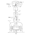
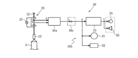
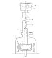
図1に示すように、本発明装置は、回転ボックス10内にウインチ11で巻上げ巻下ろされるワイヤ12の異常(ワイヤ素線の断線や曲げ、へこみ、損傷などによる形状変化や金属疲労などの内部変化)を検出するセンサ20を配設し、センサ20の検出信号に基づいて警報信号などを発信する検査監視ユニット30を製造装置内外に配備する。ワイヤ12は、例えばステンレス線又はタングステン線の素線を撚った撚り線である。センサ20は、回転ボックス10内の所定の位置に設置された渦流探傷センサで、鉛直方向に昇降するワイヤ12に接近させて配置される。以下、必要に応じてセンサ20を渦流探傷センサ20と称する。検査監視ユニット30は、例えば図4に示すように回転ボックス10内に渦流探傷センサ20(又は漏洩磁束探傷センサ)と共に設置される検査回路部30aと、回転ボックス10外に設置される監視回路部30bと、検査回路部30aと監視回路部30bの間に配置された信号送信手段30cを有する。
As shown in FIG. 1, the apparatus of the present invention has an abnormality of a
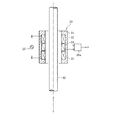
渦流探傷センサ20の構造例と動作原理図を図2と図3に示す。図2の渦流探傷センサ20は、昇降するワイヤ12を非接触で非破壊検査するもので、ワイヤ12が非接触で上下に貫通する筒状のボビン21と、ボビン21の内周の上部と下部に装着された2つの送信コイル22、23と、ボビン21の内周の中間部に装着された受信コイル24を有する。なお、図示される送信コイル22、23は貫通コイル構造であるが、半割コイル又はU字型コイル構造でもよい。
A structural example and operation principle diagram of the eddy current
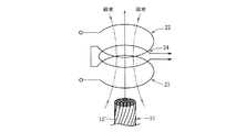
送信コイル22、23に交流発信器25から2000KHz程度の正弦波励磁電流を流すと、図3の鎖線で示すようにボビン21内に軸方向に磁束が発生し、この磁束域をワイヤ12が通過することでワイヤ12に渦電流が発生する。この渦電流はワイヤ12に異常があると、その異常に応じて変化する。この渦電流変化を受信コイル24がインピーダンス変化、或いは、誘導電圧変化として検出して検査監視ユニット30の検査回路部30aに出力する。検査回路部30aは受信コイル24からのインピーダンス変化、又は誘導電圧変化の検出信号sからノイズ成分を除去し、増幅して信号送信手段30cに送信する。信号送信手段30cは、例えば回転ボックス10に設置した送信アンテナと監視回路部30bに設置した受信アンテナを備えた無線伝送手段、又は、回転ボックス10に設置したスリップリングと、このスリップリングに電気的に接触する触子を備えた有線伝送手段で構成できる。
When a sinusoidal excitation current of about 2000 KHz is passed from the
監視回路部30bは、上記受信アンテナで受信された検出信号sからワイヤ異常の度合をアナログ又はデジタル表示するの表示器31と、検出信号sを記憶してワイヤ管理等に使用されるメモリ回路32と、検出信号sの信号レベルと所定の閾値の比較結果に基づいて適宜に警報信号tを出力する異常判定回路33を備える。異常判定回路33の出力側に警報ランプ34と、警報ブザー35の各ドライブ(図示せず)が接続される。
The
次に、上記実施例の形態の動作を説明する。 Next, the operation of the above embodiment will be described.
図1に示すように、ウインチ11を逆回転(右回転)させて単結晶インゴット5を吊り下げたワイヤ12を所定高さ位置に固定配置した渦流探傷センサ20を貫通させて上昇させる。これにより渦流探傷センサ20でワイヤ12の異常検出が連続して行われる。この間、渦流探傷センサ20からの検出信号sが検査監視ユニット30の検査回路部30aに送信され、監視回路部30bの表示器31にワイヤ異常の有無と異常度合が数値化されてアナログ又はデジタルで表示される。この表示を作業員が視認することで、現在使用されているワイヤ12が異常のあるワイヤか、異常のあるワイヤの場合はどのレベル、数、種類の異常が発生しているかが判断される。これらワイヤの異常が、放置しても問題とならないほど小さなレベルの異常である場合は、この小レベルの異常に対する検出信号sが異常判定回路33に設定された閾値を超えないようにして警報信号を発しないようにすることができる。なお、後の分析用として検出信号sはメモリー回路32に保存される。また、ワイヤの異常が、ワイヤ断線等の事故を引き起こす要因となり得る大レベルの異常の場合は、この大レベルの異常に対する検出信号sが異常判定回路33の閾値を超えて、異常判定回路33から警報信号tが出力され、警報ランプ34が点滅し、警報ブザー35が鳴り、周囲の作業員に報知される。
As shown in FIG. 1, the
この大レベルの異常は、例えば図3に示すワイヤ12を構成する多数本の素線12’の1本又は数本の断線である。撚り線のワイヤ12の断線は、1本又は数本の素線12’の断線を放置することにより発生する確率が高く、このような素線12’の断線は、ワイヤ12を流れる渦電流の大きな変化となって現れることから、1本の素線12’の断線であっても、この断線異常が渦流探傷センサ20で高精度に検出される。
This large-level abnormality is, for example, one or several breaks in the
図1において、単結晶インゴット5の引き上げが終了するまで渦流探傷センサ20によるワイヤ異常検出が継続して行われ、チャック13が渦流探傷センサ20の高さ位置まで上昇したところで引き上げを終了させて、ワイヤ12のウインチ11から吊り下がり鉛直となる部分の全長を非破壊検査する。この検査工程で検査監視ユニット30が一度も警報を発しない場合は、ワイヤ12にまったく異常がないか、あるいは異常が有ってもまだ十分に使用できるワイヤであると判定されて、同じワイヤ12が次の単結晶製造に継続して使用される。また、上記検査工程で検査監視ユニット30が警報を発すると、ワイヤ12に大レベルの異常が有り、これを放置してワイヤ12を更に何度も使用するとワイヤ断線の危険性が増すと判定される。この場合は、1回の検査工程が終了した後、ワイヤ12を新品と交換する時期が経験に基づいて決定される。
In FIG. 1, the wire abnormality detection by the eddy current
なお、本発明は上記した実施の形態に限定されるものではなく、本発明の要旨を逸脱しない範囲内において種々変更を加え得ることは勿論である。例えば、図1の単結晶製造装置はチャンバー上の回転ボックス内にセンサを配備しているが、チャンバー構造によってはチャンバー内の上部にセンサを配備するようにしてもよい。また、ワイヤを巻上げ巻下げるウインチの周面に巻回されているワイヤを対象にセンサで異常検出することも可能である。 It should be noted that the present invention is not limited to the above-described embodiment, and it is needless to say that various modifications can be made without departing from the gist of the present invention. For example, although the single crystal manufacturing apparatus in FIG. 1 has a sensor arranged in a rotating box on the chamber, the sensor may be arranged in the upper part of the chamber depending on the chamber structure. It is also possible to detect an abnormality with a sensor for the wire wound on the peripheral surface of the winch that winds and unwinds the wire.
1 チャンバー
2 るつぼ
3 ヒーター
4 原料融液
5 単結晶インゴット
10 回転ボックス
11 ウインチ
12 ワイヤ
13 チャック
20 センサ、渦流探傷センサ
21 ボビン
22、23 送信コイル
24 受信コイル
25 交流発信器
30 検査監視ユニット
30a 検査回路部
30b 監視回路部
30c 信号送信手段
31 表示器
32 メモリー回路
33 異常判定回路
34 警報ランプ
35 警報ブザー
s 検出信号
t 警報信号
DESCRIPTION OF SYMBOLS 1 Chamber 2 Crucible 3
Claims (3)
前記ウインチの近傍に、前記ワイヤの異常を検出するセンサを配設したことを特徴とする単結晶製造装置。 A crucible containing a raw material melt of a single crystal ingot; and a winch disposed above the crucible and having a seed crystal attached to a lower end thereof for winding and unwinding, the seed on the surface of the raw material melt in the crucible In a single crystal manufacturing apparatus in which a single crystal ingot is grown by bringing a crystal into contact with the crystal while pulling up with the wire,
A single crystal manufacturing apparatus, wherein a sensor for detecting an abnormality of the wire is disposed in the vicinity of the winch.
Priority Applications (1)
| Application Number | Priority Date | Filing Date | Title |
|---|---|---|---|
| JP2004038808A JP3920859B2 (en) | 2004-02-16 | 2004-02-16 | Single crystal manufacturing equipment |
Applications Claiming Priority (1)
| Application Number | Priority Date | Filing Date | Title |
|---|---|---|---|
| JP2004038808A JP3920859B2 (en) | 2004-02-16 | 2004-02-16 | Single crystal manufacturing equipment |
Publications (2)
| Publication Number | Publication Date |
|---|---|
| JP2005225741A true JP2005225741A (en) | 2005-08-25 |
| JP3920859B2 JP3920859B2 (en) | 2007-05-30 |
Family
ID=35000748
Family Applications (1)
| Application Number | Title | Priority Date | Filing Date |
|---|---|---|---|
| JP2004038808A Expired - Lifetime JP3920859B2 (en) | 2004-02-16 | 2004-02-16 | Single crystal manufacturing equipment |
Country Status (1)
| Country | Link |
|---|---|
| JP (1) | JP3920859B2 (en) |
Cited By (2)
| Publication number | Priority date | Publication date | Assignee | Title |
|---|---|---|---|---|
| WO2014075578A1 (en) * | 2012-11-14 | 2014-05-22 | 田立 | Solid liquid interface detection device for polysilicon ingot furnace |
| KR101609462B1 (en) * | 2014-08-04 | 2016-04-05 | 주식회사 엘지실트론 | Seed cable management apparatus of single crystal growth device and control method for it |
Citations (10)
| Publication number | Priority date | Publication date | Assignee | Title |
|---|---|---|---|---|
| JPS59650A (en) * | 1982-06-28 | 1984-01-05 | Hitachi Ltd | Electromagnetic flaw detector for wire rope |
| JPS6265994A (en) * | 1985-03-06 | 1987-03-25 | フエロフルイデイクス・コ−ポレイシヨン | Pulling head for crystal growing furnace |
| JPH08208378A (en) * | 1995-02-02 | 1996-08-13 | Komatsu Ltd | Feed drive device for single crystal puller |
| JPH09184824A (en) * | 1995-12-28 | 1997-07-15 | Tokyo Seiko Co Ltd | Anti-vibration probe for wire rope electromagnetic flaw detector |
| JP2000264770A (en) * | 1999-03-19 | 2000-09-26 | Toshiba Ceramics Co Ltd | Method and apparatus for evaluating seed wire |
| JP2000351575A (en) * | 1999-06-08 | 2000-12-19 | Ishikawajima Harima Heavy Ind Co Ltd | Wire rope disconnection detector |
| JP2001213692A (en) * | 2000-01-31 | 2001-08-07 | Shin Etsu Handotai Co Ltd | Single crystal manufacturing method and single crystal manufacturing equipment |
| JP2002047091A (en) * | 2000-07-31 | 2002-02-12 | Super Silicon Kenkyusho:Kk | Apparatus for and method of pulling up single crystal |
| JP2003176199A (en) * | 2001-12-06 | 2003-06-24 | Toshiba Ceramics Co Ltd | Single crystal pulling apparatus and pulling method |
| JP2004043202A (en) * | 2002-07-08 | 2004-02-12 | Shin Etsu Handotai Co Ltd | Wire rope and apparatus for drawing single crystal and process for preparing single crystal |
-
2004
- 2004-02-16 JP JP2004038808A patent/JP3920859B2/en not_active Expired - Lifetime
Patent Citations (10)
| Publication number | Priority date | Publication date | Assignee | Title |
|---|---|---|---|---|
| JPS59650A (en) * | 1982-06-28 | 1984-01-05 | Hitachi Ltd | Electromagnetic flaw detector for wire rope |
| JPS6265994A (en) * | 1985-03-06 | 1987-03-25 | フエロフルイデイクス・コ−ポレイシヨン | Pulling head for crystal growing furnace |
| JPH08208378A (en) * | 1995-02-02 | 1996-08-13 | Komatsu Ltd | Feed drive device for single crystal puller |
| JPH09184824A (en) * | 1995-12-28 | 1997-07-15 | Tokyo Seiko Co Ltd | Anti-vibration probe for wire rope electromagnetic flaw detector |
| JP2000264770A (en) * | 1999-03-19 | 2000-09-26 | Toshiba Ceramics Co Ltd | Method and apparatus for evaluating seed wire |
| JP2000351575A (en) * | 1999-06-08 | 2000-12-19 | Ishikawajima Harima Heavy Ind Co Ltd | Wire rope disconnection detector |
| JP2001213692A (en) * | 2000-01-31 | 2001-08-07 | Shin Etsu Handotai Co Ltd | Single crystal manufacturing method and single crystal manufacturing equipment |
| JP2002047091A (en) * | 2000-07-31 | 2002-02-12 | Super Silicon Kenkyusho:Kk | Apparatus for and method of pulling up single crystal |
| JP2003176199A (en) * | 2001-12-06 | 2003-06-24 | Toshiba Ceramics Co Ltd | Single crystal pulling apparatus and pulling method |
| JP2004043202A (en) * | 2002-07-08 | 2004-02-12 | Shin Etsu Handotai Co Ltd | Wire rope and apparatus for drawing single crystal and process for preparing single crystal |
Cited By (2)
| Publication number | Priority date | Publication date | Assignee | Title |
|---|---|---|---|---|
| WO2014075578A1 (en) * | 2012-11-14 | 2014-05-22 | 田立 | Solid liquid interface detection device for polysilicon ingot furnace |
| KR101609462B1 (en) * | 2014-08-04 | 2016-04-05 | 주식회사 엘지실트론 | Seed cable management apparatus of single crystal growth device and control method for it |
Also Published As
| Publication number | Publication date |
|---|---|
| JP3920859B2 (en) | 2007-05-30 |
Similar Documents
| Publication | Publication Date | Title |
|---|---|---|
| US8398766B2 (en) | Semiconductor wafer composed of monocrystalline silicon and method for producing it | |
| JP2012001387A (en) | Methods for measuring and controlling distance between lower end surface of heat-blocking member and surface of raw material melt, and method for manufacturing silicon single crystal | |
| TW201730543A (en) | Crucible inspection apparatus, crucible inspection method, vitreous silica crucible, method for manufacturing vitreous silica crucible, method for manufacturing silicon ingot, and meth od for manufacturing homoepitaxial wafer | |
| JP3920859B2 (en) | Single crystal manufacturing equipment | |
| WO2004027124A1 (en) | Thermal shield member of silicon single crystal pulling system | |
| JP6030764B2 (en) | Inspection method of silica glass crucible | |
| JP6631468B2 (en) | How to set the nozzle position of the remaining hot water suction device | |
| JP5980749B2 (en) | Anomaly detection device | |
| JPWO2002010486A1 (en) | Method for detecting the end of polycrystalline silicon melting, method for setting seed crystal temperature, and silicon single crystal manufacturing device | |
| JP4788029B2 (en) | Semiconductor single crystal manufacturing apparatus and semiconductor single crystal manufacturing method using the same | |
| CN115485228B (en) | Sling monitoring device and crane system | |
| CN212062027U (en) | Broken tape checking device for wrapping machine | |
| KR101609462B1 (en) | Seed cable management apparatus of single crystal growth device and control method for it | |
| TW444070B (en) | Apparatus for pulling up single crystals and single crystal clamping device | |
| KR101155413B1 (en) | Ingot weight measurement device of ingot growing apparatus | |
| JP6200057B2 (en) | Inspection method of silica glass crucible | |
| JP2004224585A (en) | Method and apparatus for manufacturing single crystal | |
| JP4168784B2 (en) | Single crystal manufacturing apparatus and single crystal manufacturing method | |
| JP3702672B2 (en) | Temperature measurement system for single crystal rod in puller | |
| JP2011032136A (en) | Method for monitoring height of liquid surface | |
| JP3719198B2 (en) | Single crystal bend growth detection method, single crystal bend growth detection apparatus, and single crystal manufacturing apparatus | |
| JP5696710B2 (en) | Silicon single crystal ingot | |
| JP2005082433A (en) | Apparatus for manufacturing single crystal and solidification contact monitoring method | |
| CN119780789A (en) | A method and device for detecting thermal field components of a crystal pulling furnace | |
| CN213843836U (en) | Active coke desulfurization double-valve-core discharger online detection system |
Legal Events
| Date | Code | Title | Description |
|---|---|---|---|
| A621 | Written request for application examination |
Free format text: JAPANESE INTERMEDIATE CODE: A621 Effective date: 20040216 |
|
| A977 | Report on retrieval |
Free format text: JAPANESE INTERMEDIATE CODE: A971007 Effective date: 20061012 |
|
| A131 | Notification of reasons for refusal |
Free format text: JAPANESE INTERMEDIATE CODE: A131 Effective date: 20061016 |
|
| A521 | Request for written amendment filed |
Free format text: JAPANESE INTERMEDIATE CODE: A523 Effective date: 20061212 |
|
| A521 | Request for written amendment filed |
Free format text: JAPANESE INTERMEDIATE CODE: A523 Effective date: 20061214 |
|
| A521 | Request for written amendment filed |
Free format text: JAPANESE INTERMEDIATE CODE: A523 Effective date: 20061214 |
|
| TRDD | Decision of grant or rejection written | ||
| A01 | Written decision to grant a patent or to grant a registration (utility model) |
Free format text: JAPANESE INTERMEDIATE CODE: A01 Effective date: 20070117 |
|
| A61 | First payment of annual fees (during grant procedure) |
Free format text: JAPANESE INTERMEDIATE CODE: A61 Effective date: 20070215 |
|
| R150 | Certificate of patent or registration of utility model |
Ref document number: 3920859 Country of ref document: JP Free format text: JAPANESE INTERMEDIATE CODE: R150 Free format text: JAPANESE INTERMEDIATE CODE: R150 |
|
| FPAY | Renewal fee payment (event date is renewal date of database) |
Free format text: PAYMENT UNTIL: 20100223 Year of fee payment: 3 |
|
| FPAY | Renewal fee payment (event date is renewal date of database) |
Free format text: PAYMENT UNTIL: 20110223 Year of fee payment: 4 |
|
| R250 | Receipt of annual fees |
Free format text: JAPANESE INTERMEDIATE CODE: R250 |
|
| FPAY | Renewal fee payment (event date is renewal date of database) |
Free format text: PAYMENT UNTIL: 20120223 Year of fee payment: 5 |
|
| R250 | Receipt of annual fees |
Free format text: JAPANESE INTERMEDIATE CODE: R250 |
|
| FPAY | Renewal fee payment (event date is renewal date of database) |
Free format text: PAYMENT UNTIL: 20130223 Year of fee payment: 6 |
|
| R250 | Receipt of annual fees |
Free format text: JAPANESE INTERMEDIATE CODE: R250 |
|
| FPAY | Renewal fee payment (event date is renewal date of database) |
Free format text: PAYMENT UNTIL: 20130223 Year of fee payment: 6 |
|
| S111 | Request for change of ownership or part of ownership |
Free format text: JAPANESE INTERMEDIATE CODE: R313117 |
|
| S533 | Written request for registration of change of name |
Free format text: JAPANESE INTERMEDIATE CODE: R313533 |
|
| R350 | Written notification of registration of transfer |
Free format text: JAPANESE INTERMEDIATE CODE: R350 |
|
| FPAY | Renewal fee payment (event date is renewal date of database) |
Free format text: PAYMENT UNTIL: 20130223 Year of fee payment: 6 |
|
| FPAY | Renewal fee payment (event date is renewal date of database) |
Free format text: PAYMENT UNTIL: 20140223 Year of fee payment: 7 |
|
| R250 | Receipt of annual fees |
Free format text: JAPANESE INTERMEDIATE CODE: R250 |
|
| R250 | Receipt of annual fees |
Free format text: JAPANESE INTERMEDIATE CODE: R250 |
|
| R250 | Receipt of annual fees |
Free format text: JAPANESE INTERMEDIATE CODE: R250 |
|
| R250 | Receipt of annual fees |
Free format text: JAPANESE INTERMEDIATE CODE: R250 |
|
| R250 | Receipt of annual fees |
Free format text: JAPANESE INTERMEDIATE CODE: R250 |
|
| R250 | Receipt of annual fees |
Free format text: JAPANESE INTERMEDIATE CODE: R250 |
|
| R250 | Receipt of annual fees |
Free format text: JAPANESE INTERMEDIATE CODE: R250 |
|
| R250 | Receipt of annual fees |
Free format text: JAPANESE INTERMEDIATE CODE: R250 |
|
| R250 | Receipt of annual fees |
Free format text: JAPANESE INTERMEDIATE CODE: R250 |
|
| R250 | Receipt of annual fees |
Free format text: JAPANESE INTERMEDIATE CODE: R250 |
|
| R250 | Receipt of annual fees |
Free format text: JAPANESE INTERMEDIATE CODE: R250 |
|
| EXPY | Cancellation because of completion of term |