JP2005229096A - Ldd構造を有する薄膜トランジスタ及びその製造方法 - Google Patents
Ldd構造を有する薄膜トランジスタ及びその製造方法 Download PDFInfo
- Publication number
- JP2005229096A JP2005229096A JP2004332451A JP2004332451A JP2005229096A JP 2005229096 A JP2005229096 A JP 2005229096A JP 2004332451 A JP2004332451 A JP 2004332451A JP 2004332451 A JP2004332451 A JP 2004332451A JP 2005229096 A JP2005229096 A JP 2005229096A
- Authority
- JP
- Japan
- Prior art keywords
- semiconductor layer
- film transistor
- thin film
- thickness
- region
- Prior art date
- Legal status (The legal status is an assumption and is not a legal conclusion. Google has not performed a legal analysis and makes no representation as to the accuracy of the status listed.)
- Pending
Links
Images



Classifications
-
- H—ELECTRICITY
- H10—SEMICONDUCTOR DEVICES; ELECTRIC SOLID-STATE DEVICES NOT OTHERWISE PROVIDED FOR
- H10D—INORGANIC ELECTRIC SEMICONDUCTOR DEVICES
- H10D30/00—Field-effect transistors [FET]
- H10D30/60—Insulated-gate field-effect transistors [IGFET]
- H10D30/67—Thin-film transistors [TFT]
- H10D30/6704—Thin-film transistors [TFT] having supplementary regions or layers in the thin films or in the insulated bulk substrates for controlling properties of the device
- H10D30/6713—Thin-film transistors [TFT] having supplementary regions or layers in the thin films or in the insulated bulk substrates for controlling properties of the device characterised by the properties of the source or drain regions, e.g. compositions or sectional shapes
- H10D30/6715—Thin-film transistors [TFT] having supplementary regions or layers in the thin films or in the insulated bulk substrates for controlling properties of the device characterised by the properties of the source or drain regions, e.g. compositions or sectional shapes characterised by the doping profiles, e.g. having lightly-doped source or drain extensions
-
- H—ELECTRICITY
- H10—SEMICONDUCTOR DEVICES; ELECTRIC SOLID-STATE DEVICES NOT OTHERWISE PROVIDED FOR
- H10D—INORGANIC ELECTRIC SEMICONDUCTOR DEVICES
- H10D30/00—Field-effect transistors [FET]
- H10D30/01—Manufacture or treatment
- H10D30/021—Manufacture or treatment of FETs having insulated gates [IGFET]
- H10D30/031—Manufacture or treatment of FETs having insulated gates [IGFET] of thin-film transistors [TFT]
- H10D30/0312—Manufacture or treatment of FETs having insulated gates [IGFET] of thin-film transistors [TFT] characterised by the gate electrodes
- H10D30/0314—Manufacture or treatment of FETs having insulated gates [IGFET] of thin-film transistors [TFT] characterised by the gate electrodes of lateral top-gate TFTs comprising only a single gate
-
- H—ELECTRICITY
- H10—SEMICONDUCTOR DEVICES; ELECTRIC SOLID-STATE DEVICES NOT OTHERWISE PROVIDED FOR
- H10D—INORGANIC ELECTRIC SEMICONDUCTOR DEVICES
- H10D30/00—Field-effect transistors [FET]
- H10D30/01—Manufacture or treatment
- H10D30/021—Manufacture or treatment of FETs having insulated gates [IGFET]
- H10D30/031—Manufacture or treatment of FETs having insulated gates [IGFET] of thin-film transistors [TFT]
- H10D30/0321—Manufacture or treatment of FETs having insulated gates [IGFET] of thin-film transistors [TFT] comprising silicon, e.g. amorphous silicon or polysilicon
Landscapes
- Thin Film Transistor (AREA)
Abstract
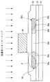
【解決手段】 薄膜トランジスタは、ソース/ドレイン領域、該ソース/ドレイン領域間に位置するチャンネル領域および該チャンネルと該ソース/ドレイン領域との間に位置するLDD領域を備える半導体層を含み、該LDD領域はドーピングされたイオンの投射範囲(Projected Range)Rpが前記半導体層の表面から第1深さに位置する。これにより、チャンネルの信頼性と共にアウトプット特性が改善された薄膜トランジスタを得ることができる。
【選択図】 図1B
Description
[数式1]
(前記半導体層の厚さ/2)−100Å≦第1深さ≦(前記半導体層の厚さ/2)+100Å
20 半導体層
20a ソース/ドレイン領域
20b LDD領域
30、31 ゲート絶縁膜
Claims (10)
- ソース領域、ドレイン領域、該ソース領域と該ドレイン領域との間に位置したチャンネル領域、及び該チャンネル領域と該ドレイン領域との間に位置するLDD領域、を備える半導体層を含み、
前記LDD領域は、ドーピングされたイオンの投射範囲が前記半導体層の表面から第1深さに位置することを特徴とする薄膜トランジスタ。 - 前記第1深さは、下記数式1を満足することを特徴とする請求項1に記載の薄膜トランジスタ。
<数式1>
(前記半導体層の厚さ/2)−100Å≦第1深さ≦(前記半導体層の厚さ/2)+100Å - 前記半導体層は、ELA方式、またはSLS方式を使用して結晶化されたことを特徴とする請求項1に記載の薄膜トランジスタ。
- 前記半導体層上に位置し、前記LDD領域上の厚さが前記チャンネル領域上の厚さに比べて第1厚さほど低いゲート絶縁膜と、
前記ゲート絶縁膜上に位置するゲート電極と、
をさらに含むことを特徴とする請求項1に記載の薄膜トランジスタ。 - 前記第1厚さは、前記第1深さと同じ大きさであることを特徴とする請求項1に記載の薄膜トランジスタ。
- 基板上に半導体層を形成する段階と、
前記半導体層上にゲート絶縁膜を形成する段階と、
前記ゲート絶縁膜上にゲート電極を形成する段階と、
前記ゲート電極周辺のゲート絶縁膜を第1厚さほどエッチングする段階と、
前記ゲート電極をマスクとして、前記半導体層にイオンドーピングすることによって、ドーピングされたイオンの投射範囲が前記半導体層の表面から第1深さに位置するLDD領域を形成する段階と、
を含むことを特徴とする薄膜トランジスタの製造方法。 - 前記第1深さは、下記数式1を満足することを特徴とする請求項6に記載の薄膜トランジスタの製造方法。
<数式1>
(前記半導体層の厚さ/2)−100Å≦第1深さ≦(前記半導体層の厚さ/2)+100Å - 前記第1厚さは、前記第1深さと同じ大きさを有することを特徴とする請求項6に記載の薄膜トランジスタの製造方法。
- 前記LDD領域を形成するイオンドーピングは、80ないし90KeVの加速電圧条件で実施することを特徴とする請求項6に記載の薄膜トランジスタ製造方法。
- 前記LDD領域を形成するイオンドーピングは、1E13ないし5E13ions/cm2のドーズ条件で実施することを特徴とする請求項6に記載の薄膜トランジスタ製造方法。
Applications Claiming Priority (1)
| Application Number | Priority Date | Filing Date | Title |
|---|---|---|---|
| KR1020040009378A KR100579188B1 (ko) | 2004-02-12 | 2004-02-12 | 엘디디 구조를 갖는 박막트랜지스터 |
Publications (1)
| Publication Number | Publication Date |
|---|---|
| JP2005229096A true JP2005229096A (ja) | 2005-08-25 |
Family
ID=34836725
Family Applications (1)
| Application Number | Title | Priority Date | Filing Date |
|---|---|---|---|
| JP2004332451A Pending JP2005229096A (ja) | 2004-02-12 | 2004-11-16 | Ldd構造を有する薄膜トランジスタ及びその製造方法 |
Country Status (4)
| Country | Link |
|---|---|
| US (2) | US7247883B2 (ja) |
| JP (1) | JP2005229096A (ja) |
| KR (1) | KR100579188B1 (ja) |
| CN (1) | CN1655366B (ja) |
Cited By (6)
| Publication number | Priority date | Publication date | Assignee | Title |
|---|---|---|---|---|
| JP2007311495A (ja) * | 2006-05-17 | 2007-11-29 | Mitsubishi Electric Corp | 半導体装置の製造方法 |
| JP2009038076A (ja) * | 2007-07-31 | 2009-02-19 | National Institute Of Advanced Industrial & Technology | 二重絶縁ゲート電界効果トランジスタ |
| JP2010232635A (ja) * | 2009-03-27 | 2010-10-14 | Samsung Mobile Display Co Ltd | 薄膜トランジスタ及びその製造方法、並びにそれを含む有機電界発光表示装置 |
| US8409887B2 (en) | 2009-03-03 | 2013-04-02 | Samsung Display Co., Ltd. | Organic light emitting diode display device and method of fabricating the same |
| US8546248B2 (en) | 2009-03-05 | 2013-10-01 | Samsung Display Co., Ltd. | Method of forming polycrystalline silicon layer and atomic layer deposition apparatus used for the same |
| US8890165B2 (en) | 2009-11-13 | 2014-11-18 | Samsung Display Co., Ltd. | Method of forming polycrystalline silicon layer, thin film transistor, organic light emitting diode display device having the same, and methods of fabricating the same |
Families Citing this family (9)
| Publication number | Priority date | Publication date | Assignee | Title |
|---|---|---|---|---|
| KR101043785B1 (ko) * | 2008-12-08 | 2011-06-22 | 주식회사 엔씰텍 | 박막트랜지스터 및 그의 제조방법 |
| CN102646593A (zh) * | 2011-05-16 | 2012-08-22 | 京东方科技集团股份有限公司 | 一种tft及tft的制造方法 |
| CN103811559B (zh) * | 2014-02-21 | 2018-07-06 | 苏州大学 | 一种具有双极型工作特性的薄膜晶体管 |
| CN104143533B (zh) * | 2014-08-07 | 2017-06-27 | 深圳市华星光电技术有限公司 | 高解析度amoled背板制造方法 |
| KR102822240B1 (ko) | 2019-07-30 | 2025-06-20 | 삼성디스플레이 주식회사 | 표시 장치 및 그의 제조 방법 |
| KR102886219B1 (ko) | 2021-02-17 | 2025-11-17 | 삼성디스플레이 주식회사 | 표시 장치 |
| KR102831368B1 (ko) | 2021-09-09 | 2025-07-09 | 삼성디스플레이 주식회사 | 표시 장치, 이의 제조 방법, 및 이를 포함하는 전자 기기 |
| KR20230097252A (ko) | 2021-12-23 | 2023-07-03 | 삼성디스플레이 주식회사 | 표시 장치 |
| KR20240074139A (ko) | 2022-11-18 | 2024-05-28 | 삼성디스플레이 주식회사 | 표시 장치 |
Citations (10)
| Publication number | Priority date | Publication date | Assignee | Title |
|---|---|---|---|---|
| JPH0320046A (ja) * | 1989-06-16 | 1991-01-29 | Matsushita Electron Corp | 半導体装置の製造方法 |
| JPH04186734A (ja) * | 1990-11-20 | 1992-07-03 | Seiko Epson Corp | 半導体装置の製造方法 |
| JPH04299834A (ja) * | 1991-03-28 | 1992-10-23 | Sanyo Electric Co Ltd | Mos型半導体装置の製造方法 |
| JPH05152328A (ja) * | 1991-11-28 | 1993-06-18 | Casio Comput Co Ltd | 薄膜トランジスタの製造方法 |
| JPH06342808A (ja) * | 1993-05-31 | 1994-12-13 | Sanyo Electric Co Ltd | 薄膜トランジスタの製造方法 |
| JPH07211912A (ja) * | 1994-01-21 | 1995-08-11 | Fuji Xerox Co Ltd | 薄膜トランジスタ及びその製造方法 |
| JPH08111390A (ja) * | 1994-10-07 | 1996-04-30 | Ricoh Co Ltd | Mos半導体装置の製造方法 |
| JPH10256557A (ja) * | 1997-03-14 | 1998-09-25 | Toshiba Corp | 薄膜トランジスタおよび液晶表示装置 |
| WO2001029898A1 (en) * | 1999-10-21 | 2001-04-26 | Matsushita Electric Industrial Co., Ltd. | Thin-film transistor, method of manufacture thereof, and thin-film transistor lcd |
| JP2002185008A (ja) * | 2000-12-19 | 2002-06-28 | Hitachi Ltd | 薄膜トランジスタ |
Family Cites Families (7)
| Publication number | Priority date | Publication date | Assignee | Title |
|---|---|---|---|---|
| KR950021242A (ko) * | 1993-12-28 | 1995-07-26 | 김광호 | 다결정 실리콘 박막 트랜지스터 및 그 제조 방법 |
| US6127211A (en) * | 1997-10-02 | 2000-10-03 | Matsushita Electric Industrial Co., Ltd. | Method of manufacturing transistor |
| KR100640207B1 (ko) | 1999-10-29 | 2006-10-31 | 엘지.필립스 엘시디 주식회사 | 박막트랜지스터 및 그 제조방법 |
| JP4037117B2 (ja) * | 2001-02-06 | 2008-01-23 | 株式会社日立製作所 | 表示装置 |
| US6833313B2 (en) * | 2001-04-13 | 2004-12-21 | Semiconductor Energy Laboratory Co., Ltd. | Method of manufacturing semiconductor device by implanting rare gas ions |
| KR100405080B1 (ko) | 2001-05-11 | 2003-11-10 | 엘지.필립스 엘시디 주식회사 | 실리콘 결정화방법. |
| US7416927B2 (en) * | 2002-03-26 | 2008-08-26 | Infineon Technologies Ag | Method for producing an SOI field effect transistor |
-
2004
- 2004-02-12 KR KR1020040009378A patent/KR100579188B1/ko not_active Expired - Lifetime
- 2004-11-16 JP JP2004332451A patent/JP2005229096A/ja active Pending
-
2005
- 2005-01-21 US US11/038,031 patent/US7247883B2/en not_active Expired - Lifetime
- 2005-02-07 CN CN200510008029.5A patent/CN1655366B/zh not_active Expired - Lifetime
-
2007
- 2007-06-26 US US11/768,332 patent/US7491591B2/en not_active Expired - Lifetime
Patent Citations (10)
| Publication number | Priority date | Publication date | Assignee | Title |
|---|---|---|---|---|
| JPH0320046A (ja) * | 1989-06-16 | 1991-01-29 | Matsushita Electron Corp | 半導体装置の製造方法 |
| JPH04186734A (ja) * | 1990-11-20 | 1992-07-03 | Seiko Epson Corp | 半導体装置の製造方法 |
| JPH04299834A (ja) * | 1991-03-28 | 1992-10-23 | Sanyo Electric Co Ltd | Mos型半導体装置の製造方法 |
| JPH05152328A (ja) * | 1991-11-28 | 1993-06-18 | Casio Comput Co Ltd | 薄膜トランジスタの製造方法 |
| JPH06342808A (ja) * | 1993-05-31 | 1994-12-13 | Sanyo Electric Co Ltd | 薄膜トランジスタの製造方法 |
| JPH07211912A (ja) * | 1994-01-21 | 1995-08-11 | Fuji Xerox Co Ltd | 薄膜トランジスタ及びその製造方法 |
| JPH08111390A (ja) * | 1994-10-07 | 1996-04-30 | Ricoh Co Ltd | Mos半導体装置の製造方法 |
| JPH10256557A (ja) * | 1997-03-14 | 1998-09-25 | Toshiba Corp | 薄膜トランジスタおよび液晶表示装置 |
| WO2001029898A1 (en) * | 1999-10-21 | 2001-04-26 | Matsushita Electric Industrial Co., Ltd. | Thin-film transistor, method of manufacture thereof, and thin-film transistor lcd |
| JP2002185008A (ja) * | 2000-12-19 | 2002-06-28 | Hitachi Ltd | 薄膜トランジスタ |
Cited By (8)
| Publication number | Priority date | Publication date | Assignee | Title |
|---|---|---|---|---|
| JP2007311495A (ja) * | 2006-05-17 | 2007-11-29 | Mitsubishi Electric Corp | 半導体装置の製造方法 |
| JP2009038076A (ja) * | 2007-07-31 | 2009-02-19 | National Institute Of Advanced Industrial & Technology | 二重絶縁ゲート電界効果トランジスタ |
| US8409887B2 (en) | 2009-03-03 | 2013-04-02 | Samsung Display Co., Ltd. | Organic light emitting diode display device and method of fabricating the same |
| US9035311B2 (en) | 2009-03-03 | 2015-05-19 | Samsung Display Co., Ltd. | Organic light emitting diode display device and method of fabricating the same |
| US8546248B2 (en) | 2009-03-05 | 2013-10-01 | Samsung Display Co., Ltd. | Method of forming polycrystalline silicon layer and atomic layer deposition apparatus used for the same |
| JP2010232635A (ja) * | 2009-03-27 | 2010-10-14 | Samsung Mobile Display Co Ltd | 薄膜トランジスタ及びその製造方法、並びにそれを含む有機電界発光表示装置 |
| US9117798B2 (en) | 2009-03-27 | 2015-08-25 | Samsung Display Co., Ltd. | Thin film transistor, method of fabricating the same and organic light emitting diode display device including the same |
| US8890165B2 (en) | 2009-11-13 | 2014-11-18 | Samsung Display Co., Ltd. | Method of forming polycrystalline silicon layer, thin film transistor, organic light emitting diode display device having the same, and methods of fabricating the same |
Also Published As
| Publication number | Publication date |
|---|---|
| US7247883B2 (en) | 2007-07-24 |
| CN1655366B (zh) | 2012-05-23 |
| US20070249108A1 (en) | 2007-10-25 |
| US20050179038A1 (en) | 2005-08-18 |
| US7491591B2 (en) | 2009-02-17 |
| CN1655366A (zh) | 2005-08-17 |
| KR100579188B1 (ko) | 2006-05-11 |
| KR20050081227A (ko) | 2005-08-18 |
Similar Documents
| Publication | Publication Date | Title |
|---|---|---|
| US7491591B2 (en) | Thin film transistor having LDD structure | |
| US7821011B2 (en) | Insulated gate field effect semiconductor devices and method of manufacturing the same | |
| US6838322B2 (en) | Method for forming a double-gated semiconductor device | |
| US7338845B2 (en) | Fabrication method of a low-temperature polysilicon thin film transistor | |
| US20200098862A1 (en) | Metal source/drain-based mosfet and method for fabricating the same | |
| KR20140148296A (ko) | 박막 트랜지스터 | |
| JP2005228819A (ja) | 半導体装置 | |
| US10916641B2 (en) | Thin film transistor, method of manufacturing thin film transistor, and manufacturing system | |
| JP2007287945A (ja) | 薄膜トランジスタ | |
| US20100207120A1 (en) | Production method of semiconductor device and semiconductor device | |
| Zhou et al. | Study of the characteristics of solid phase crystallized bridged-grain poly-Si TFTs | |
| CN100570836C (zh) | 多晶硅薄膜晶体管及其制造方法 | |
| JP3501977B2 (ja) | 半導体装置 | |
| KR100914973B1 (ko) | 반도체 소자의 형성방법 | |
| JP2842112B2 (ja) | 薄膜トランジスタの製造方法 | |
| KR100649822B1 (ko) | Bc pmosfet 및 그 제조방법 | |
| KR20120044800A (ko) | 반도체 소자 및 이의 제조 방법 | |
| JP3494280B2 (ja) | 絶縁ゲイト型電界効果半導体装置 | |
| KR100600869B1 (ko) | Ldd 영역 및 goldd 영역을 구비하는박막트랜지스터 | |
| JP3380546B2 (ja) | 半導体装置 | |
| CN107611123B (zh) | 直接带隙GeSn互补型TFET | |
| KR100228334B1 (ko) | 반도체 장치의 전계효과트랜지스터 제조방법 | |
| JP2000031498A (ja) | 半導体装置 | |
| US20080217689A1 (en) | Semiconductor devices having silicon-on-insulator (soi) substrates and methods of manufacturing the same | |
| KR20040005004A (ko) | 트랜지스터 제조 방법 |
Legal Events
| Date | Code | Title | Description |
|---|---|---|---|
| A977 | Report on retrieval |
Free format text: JAPANESE INTERMEDIATE CODE: A971007 Effective date: 20061012 |
|
| A131 | Notification of reasons for refusal |
Free format text: JAPANESE INTERMEDIATE CODE: A131 Effective date: 20080507 |
|
| A601 | Written request for extension of time |
Free format text: JAPANESE INTERMEDIATE CODE: A601 Effective date: 20080807 |
|
| A602 | Written permission of extension of time |
Free format text: JAPANESE INTERMEDIATE CODE: A602 Effective date: 20080812 |
|
| A521 | Request for written amendment filed |
Free format text: JAPANESE INTERMEDIATE CODE: A523 Effective date: 20080826 |
|
| A711 | Notification of change in applicant |
Free format text: JAPANESE INTERMEDIATE CODE: A712 Effective date: 20081208 |
|
| A521 | Request for written amendment filed |
Free format text: JAPANESE INTERMEDIATE CODE: A523 Effective date: 20090225 |
|
| A131 | Notification of reasons for refusal |
Free format text: JAPANESE INTERMEDIATE CODE: A131 Effective date: 20090324 |
|
| A521 | Request for written amendment filed |
Free format text: JAPANESE INTERMEDIATE CODE: A523 Effective date: 20090624 |
|
| A02 | Decision of refusal |
Free format text: JAPANESE INTERMEDIATE CODE: A02 Effective date: 20100423 |