JP2005290196A - Phosphor material, phosphor thin film and its manufacturing method, light-emitting element, and el device - Google Patents
Phosphor material, phosphor thin film and its manufacturing method, light-emitting element, and el device Download PDFInfo
- Publication number
- JP2005290196A JP2005290196A JP2004106934A JP2004106934A JP2005290196A JP 2005290196 A JP2005290196 A JP 2005290196A JP 2004106934 A JP2004106934 A JP 2004106934A JP 2004106934 A JP2004106934 A JP 2004106934A JP 2005290196 A JP2005290196 A JP 2005290196A
- Authority
- JP
- Japan
- Prior art keywords
- phosphor
- group
- metal
- thin film
- layer
- Prior art date
- Legal status (The legal status is an assumption and is not a legal conclusion. Google has not performed a legal analysis and makes no representation as to the accuracy of the status listed.)
- Pending
Links
- OAICVXFJPJFONN-UHFFFAOYSA-N Phosphorus Chemical compound [P] OAICVXFJPJFONN-UHFFFAOYSA-N 0.000 title claims abstract description 243
- 239000000463 material Substances 0.000 title claims abstract description 155
- 239000010409 thin film Substances 0.000 title claims abstract description 70
- 238000004519 manufacturing process Methods 0.000 title claims abstract description 28
- 229910052751 metal Inorganic materials 0.000 claims abstract description 53
- 239000002184 metal Substances 0.000 claims abstract description 51
- 229910052783 alkali metal Inorganic materials 0.000 claims abstract description 27
- 150000001340 alkali metals Chemical class 0.000 claims abstract description 26
- 229910052761 rare earth metal Inorganic materials 0.000 claims abstract description 25
- 229910052723 transition metal Inorganic materials 0.000 claims abstract description 25
- 150000002910 rare earth metals Chemical class 0.000 claims abstract description 23
- 150000003624 transition metals Chemical class 0.000 claims abstract description 23
- 229910052795 boron group element Inorganic materials 0.000 claims abstract description 20
- 229910052717 sulfur Inorganic materials 0.000 claims abstract description 18
- NINIDFKCEFEMDL-UHFFFAOYSA-N Sulfur Chemical compound [S] NINIDFKCEFEMDL-UHFFFAOYSA-N 0.000 claims abstract description 17
- 229910052736 halogen Inorganic materials 0.000 claims abstract description 17
- 150000002367 halogens Chemical class 0.000 claims abstract description 17
- 239000011593 sulfur Substances 0.000 claims abstract description 17
- 238000000137 annealing Methods 0.000 claims description 54
- 239000000203 mixture Substances 0.000 claims description 54
- 238000000034 method Methods 0.000 claims description 50
- 239000002994 raw material Substances 0.000 claims description 35
- 238000000151 deposition Methods 0.000 claims description 26
- 150000004820 halides Chemical class 0.000 claims description 25
- 230000008021 deposition Effects 0.000 claims description 15
- 230000008569 process Effects 0.000 claims description 12
- 238000010549 co-Evaporation Methods 0.000 claims description 2
- 239000000758 substrate Substances 0.000 abstract description 31
- 238000009413 insulation Methods 0.000 abstract description 4
- 238000005401 electroluminescence Methods 0.000 description 90
- KWGKDLIKAYFUFQ-UHFFFAOYSA-M lithium chloride Chemical compound [Li+].[Cl-] KWGKDLIKAYFUFQ-UHFFFAOYSA-M 0.000 description 22
- 238000005259 measurement Methods 0.000 description 19
- 238000001704 evaporation Methods 0.000 description 12
- 230000000052 comparative effect Effects 0.000 description 11
- 239000008188 pellet Substances 0.000 description 11
- 230000008020 evaporation Effects 0.000 description 10
- 239000010408 film Substances 0.000 description 10
- 239000011521 glass Substances 0.000 description 10
- 238000007740 vapor deposition Methods 0.000 description 10
- 230000015572 biosynthetic process Effects 0.000 description 8
- 238000010894 electron beam technology Methods 0.000 description 8
- 150000001875 compounds Chemical class 0.000 description 7
- 230000000694 effects Effects 0.000 description 7
- 238000010438 heat treatment Methods 0.000 description 7
- 239000013078 crystal Substances 0.000 description 6
- 238000005137 deposition process Methods 0.000 description 6
- 229910018072 Al 2 O 3 Inorganic materials 0.000 description 5
- 229910015999 BaAl Inorganic materials 0.000 description 5
- 229910052693 Europium Inorganic materials 0.000 description 5
- 239000000843 powder Substances 0.000 description 5
- 239000000126 substance Substances 0.000 description 5
- MCMNRKCIXSYSNV-UHFFFAOYSA-N Zirconium dioxide Chemical compound O=[Zr]=O MCMNRKCIXSYSNV-UHFFFAOYSA-N 0.000 description 4
- 238000007792 addition Methods 0.000 description 4
- 239000012298 atmosphere Substances 0.000 description 4
- 229910010293 ceramic material Inorganic materials 0.000 description 4
- 229910052684 Cerium Inorganic materials 0.000 description 3
- 239000000654 additive Substances 0.000 description 3
- 230000000996 additive effect Effects 0.000 description 3
- 239000003513 alkali Substances 0.000 description 3
- 230000008859 change Effects 0.000 description 3
- 239000003086 colorant Substances 0.000 description 3
- 239000004020 conductor Substances 0.000 description 3
- 238000009616 inductively coupled plasma Methods 0.000 description 3
- 238000002347 injection Methods 0.000 description 3
- 239000007924 injection Substances 0.000 description 3
- 239000012212 insulator Substances 0.000 description 3
- 230000001590 oxidative effect Effects 0.000 description 3
- 230000001737 promoting effect Effects 0.000 description 3
- 238000003980 solgel method Methods 0.000 description 3
- 229910045601 alloy Inorganic materials 0.000 description 2
- 239000000956 alloy Substances 0.000 description 2
- 239000002585 base Substances 0.000 description 2
- 239000000919 ceramic Substances 0.000 description 2
- 238000006243 chemical reaction Methods 0.000 description 2
- 239000000470 constituent Substances 0.000 description 2
- 238000009792 diffusion process Methods 0.000 description 2
- 230000005284 excitation Effects 0.000 description 2
- 238000010304 firing Methods 0.000 description 2
- 239000002241 glass-ceramic Substances 0.000 description 2
- 125000005843 halogen group Chemical group 0.000 description 2
- 239000007769 metal material Substances 0.000 description 2
- 238000002156 mixing Methods 0.000 description 2
- 229910000510 noble metal Inorganic materials 0.000 description 2
- 229910052763 palladium Inorganic materials 0.000 description 2
- 229910052697 platinum Inorganic materials 0.000 description 2
- 238000004544 sputter deposition Methods 0.000 description 2
- 229910002710 Au-Pd Inorganic materials 0.000 description 1
- 229910000906 Bronze Inorganic materials 0.000 description 1
- 229910052692 Dysprosium Inorganic materials 0.000 description 1
- 229910052691 Erbium Inorganic materials 0.000 description 1
- 229910052688 Gadolinium Inorganic materials 0.000 description 1
- 229910052689 Holmium Inorganic materials 0.000 description 1
- 229910052779 Neodymium Inorganic materials 0.000 description 1
- 229910002668 Pd-Cu Inorganic materials 0.000 description 1
- 229910052777 Praseodymium Inorganic materials 0.000 description 1
- 229910052581 Si3N4 Inorganic materials 0.000 description 1
- 229910004298 SiO 2 Inorganic materials 0.000 description 1
- VYPSYNLAJGMNEJ-UHFFFAOYSA-N Silicium dioxide Chemical compound O=[Si]=O VYPSYNLAJGMNEJ-UHFFFAOYSA-N 0.000 description 1
- XUIMIQQOPSSXEZ-UHFFFAOYSA-N Silicon Chemical compound [Si] XUIMIQQOPSSXEZ-UHFFFAOYSA-N 0.000 description 1
- 229910006404 SnO 2 Inorganic materials 0.000 description 1
- 229910052771 Terbium Inorganic materials 0.000 description 1
- 229910052775 Thulium Inorganic materials 0.000 description 1
- 229910052769 Ytterbium Inorganic materials 0.000 description 1
- -1 ZnS: Tm Chemical compound 0.000 description 1
- 230000009471 action Effects 0.000 description 1
- 239000012190 activator Substances 0.000 description 1
- 229910052782 aluminium Inorganic materials 0.000 description 1
- PNEYBMLMFCGWSK-UHFFFAOYSA-N aluminium oxide Inorganic materials [O-2].[O-2].[O-2].[Al+3].[Al+3] PNEYBMLMFCGWSK-UHFFFAOYSA-N 0.000 description 1
- 125000004429 atom Chemical group 0.000 description 1
- 239000010953 base metal Substances 0.000 description 1
- 239000011230 binding agent Substances 0.000 description 1
- 229910052797 bismuth Inorganic materials 0.000 description 1
- JCXGWMGPZLAOME-UHFFFAOYSA-N bismuth atom Chemical compound [Bi] JCXGWMGPZLAOME-UHFFFAOYSA-N 0.000 description 1
- 239000010974 bronze Substances 0.000 description 1
- 239000000969 carrier Substances 0.000 description 1
- 238000005229 chemical vapour deposition Methods 0.000 description 1
- 239000002131 composite material Substances 0.000 description 1
- 229910052802 copper Inorganic materials 0.000 description 1
- KUNSUQLRTQLHQQ-UHFFFAOYSA-N copper tin Chemical compound [Cu].[Sn] KUNSUQLRTQLHQQ-UHFFFAOYSA-N 0.000 description 1
- 238000002425 crystallisation Methods 0.000 description 1
- 230000008025 crystallization Effects 0.000 description 1
- 238000000354 decomposition reaction Methods 0.000 description 1
- 239000003989 dielectric material Substances 0.000 description 1
- 238000001035 drying Methods 0.000 description 1
- 230000001747 exhibiting effect Effects 0.000 description 1
- 239000000945 filler Substances 0.000 description 1
- 239000007789 gas Substances 0.000 description 1
- 229910052737 gold Inorganic materials 0.000 description 1
- 229910052739 hydrogen Inorganic materials 0.000 description 1
- 239000001257 hydrogen Substances 0.000 description 1
- 125000004435 hydrogen atom Chemical class [H]* 0.000 description 1
- 229910010272 inorganic material Inorganic materials 0.000 description 1
- 239000011147 inorganic material Substances 0.000 description 1
- 239000011810 insulating material Substances 0.000 description 1
- 230000003993 interaction Effects 0.000 description 1
- 229910052741 iridium Inorganic materials 0.000 description 1
- 230000001678 irradiating effect Effects 0.000 description 1
- 229910052746 lanthanum Inorganic materials 0.000 description 1
- 229910052745 lead Inorganic materials 0.000 description 1
- WABPQHHGFIMREM-UHFFFAOYSA-N lead(0) Chemical class [Pb] WABPQHHGFIMREM-UHFFFAOYSA-N 0.000 description 1
- 239000004973 liquid crystal related substance Substances 0.000 description 1
- 238000001755 magnetron sputter deposition Methods 0.000 description 1
- 229910052748 manganese Inorganic materials 0.000 description 1
- 239000011159 matrix material Substances 0.000 description 1
- 230000008018 melting Effects 0.000 description 1
- 238000002844 melting Methods 0.000 description 1
- 150000002739 metals Chemical class 0.000 description 1
- 230000005012 migration Effects 0.000 description 1
- 238000013508 migration Methods 0.000 description 1
- 239000011368 organic material Substances 0.000 description 1
- 230000010355 oscillation Effects 0.000 description 1
- SIWVEOZUMHYXCS-UHFFFAOYSA-N oxo(oxoyttriooxy)yttrium Chemical compound O=[Y]O[Y]=O SIWVEOZUMHYXCS-UHFFFAOYSA-N 0.000 description 1
- BPUBBGLMJRNUCC-UHFFFAOYSA-N oxygen(2-);tantalum(5+) Chemical compound [O-2].[O-2].[O-2].[O-2].[O-2].[Ta+5].[Ta+5] BPUBBGLMJRNUCC-UHFFFAOYSA-N 0.000 description 1
- 238000005424 photoluminescence Methods 0.000 description 1
- 238000002360 preparation method Methods 0.000 description 1
- 230000002265 prevention Effects 0.000 description 1
- 230000009257 reactivity Effects 0.000 description 1
- 230000002040 relaxant effect Effects 0.000 description 1
- 229910052706 scandium Inorganic materials 0.000 description 1
- 229910052711 selenium Inorganic materials 0.000 description 1
- 229910052710 silicon Inorganic materials 0.000 description 1
- 239000010703 silicon Substances 0.000 description 1
- HQVNEWCFYHHQES-UHFFFAOYSA-N silicon nitride Chemical compound N12[Si]34N5[Si]62N3[Si]51N64 HQVNEWCFYHHQES-UHFFFAOYSA-N 0.000 description 1
- 229910052814 silicon oxide Inorganic materials 0.000 description 1
- 229910052709 silver Inorganic materials 0.000 description 1
- 238000005245 sintering Methods 0.000 description 1
- 239000002904 solvent Substances 0.000 description 1
- VEALVRVVWBQVSL-UHFFFAOYSA-N strontium titanate Chemical compound [Sr+2].[O-][Ti]([O-])=O VEALVRVVWBQVSL-UHFFFAOYSA-N 0.000 description 1
- 238000002834 transmittance Methods 0.000 description 1
- 239000012780 transparent material Substances 0.000 description 1
- WFKWXMTUELFFGS-UHFFFAOYSA-N tungsten Chemical compound [W] WFKWXMTUELFFGS-UHFFFAOYSA-N 0.000 description 1
- 229910052721 tungsten Inorganic materials 0.000 description 1
- 239000010937 tungsten Substances 0.000 description 1
- 229910052727 yttrium Inorganic materials 0.000 description 1
Images


Landscapes
- Luminescent Compositions (AREA)
- Electroluminescent Light Sources (AREA)
Abstract
Description
本発明は、蛍光体材料、これを用いた蛍光体薄膜及びその製造方法、これを備える発光素子及びEL(電界発光;Electro Luminescence)素子に関する。 The present invention relates to a phosphor material, a phosphor thin film using the phosphor material, a method for producing the phosphor material, a light emitting device including the phosphor material, and an EL (Electro Luminescence) device.
EL素子は、蛍光体の構成材料の相違により無機EL素子と有機EL素子とに大別される。一般に、蛍光体に無機材料を用いる無機EL素子は、有機材料を用いる有機EL素子と比較して耐久性や発光寿命の点で優れた特性を有している。この無機EL素子としては、互いに対向する2つの電極の間に配置された一対の絶縁層間に蛍光体薄膜を備える、いわゆる2重絶縁型構造のEL素子が広く知られている。そして、時計やLCD(液晶ディスプレイ)等のバックライト、或いは車載モニタ等として用いられている。 EL elements are broadly classified into inorganic EL elements and organic EL elements depending on the constituent materials of the phosphor. In general, an inorganic EL element using an inorganic material for a phosphor has excellent characteristics in terms of durability and light emission lifetime as compared with an organic EL element using an organic material. As this inorganic EL element, an EL element having a so-called double insulation type structure, in which a phosphor thin film is provided between a pair of insulating layers arranged between two electrodes facing each other, is widely known. And it is used as backlights, such as a clock and LCD (liquid crystal display), or a vehicle-mounted monitor.
このような無機EL素子は、上述したような優れた特性を有しているがゆえに、コンピュータやテレビ等のディスプレイ用途への適用が期待されている。無機EL素子をこれらのディスプレイ用途に用いるためにはカラー化が必須であることから、かかるカラー化を達成するために、赤色(R)、緑色(G)及び青色(B)の3原色に対応して発光する蛍光体の探求が盛んになされている。 Such an inorganic EL element has excellent characteristics as described above, and therefore is expected to be applied to display applications such as computers and televisions. In order to use inorganic EL elements for these display applications, colorization is essential, and in order to achieve such colorization, the three primary colors of red (R), green (G), and blue (B) are supported. Thus, the search for phosphors that emit light is actively pursued.
例えば、青色蛍光体としては、母体材料がSrSであり、発光中心がCeであるもの(以下、「SrS:Ce」のように表記する。)や、ZnS:Tm等、赤色蛍光体としては、ZnS:SmやCaS:Eu等、緑色蛍光体としてはZnS:Tb、CaS:Ce等が知られている。 For example, as a blue phosphor, a host material is SrS and a light emission center is Ce (hereinafter referred to as “SrS: Ce”), a red phosphor such as ZnS: Tm, ZnS: Tb, CaS: Ce, and the like are known as green phosphors such as ZnS: Sm and CaS: Eu.
ところで、EL素子に用いられるこれらの蛍光体に必要とされる重要な特性の一つとして、発光の強度(輝度)がある。各蛍光体が高い発光輝度を有していると、これを用いたディスプレイは、その表示内容の視認性が良好となり、よって極めて実用性の高いものとなる。蛍光体の発光輝度は、通常、EL素子に印加する電圧を大きくすることで増大させることができるが、省電力化や素子の高寿命化等の観点からは、より低い電圧でより大きな発光輝度を達成できるものが望まれている。 By the way, one of the important characteristics required for these phosphors used in EL elements is the intensity (luminance) of light emission. If each phosphor has high light emission luminance, a display using the phosphor has good visibility of the display content, and thus becomes extremely practical. The light emission luminance of the phosphor can be increased by increasing the voltage applied to the EL element. However, from the viewpoint of power saving and long life of the element, the light emission luminance is higher at a lower voltage. The thing which can achieve is desired.
このような高輝度発光が可能な蛍光体としては、例えば、特許文献1に記載されているような、蛍光体材料(例えばZnS:Mn)中に、ハロゲン化アルカリ(例えばKClやKBr)を更に添加したものが知られている。そして、当該文献においては、このようにハロゲン化アルカリを添加することで、蛍光体材料を単独で用いた場合よりも高い発光輝度を達成できることが示されている。 As such a phosphor capable of high-luminance emission, for example, an alkali halide (for example, KCl or KBr) is further added to a phosphor material (for example, ZnS: Mn) as described in Patent Document 1. Additions are known. And in the said literature, it is shown that emission luminance higher than the case where a fluorescent material is used independently can be achieved by adding an alkali halide in this way.
しかしながら、これまで、上述のような手段により高輝度発光が達成された素子としては、赤色及び緑色蛍光体を備えたものに限られていた。すなわち上記3原色に対応して発光する蛍光体のうち、青色蛍光体だけは、上述のものをはじめとする従来の手段によっても、十分に高い発光輝度を達成できるものが得られていなかった。このため、従来、上記3原色を高輝度で発光できる蛍光体をそろえることが困難であり、これらのEL素子を用いて作製したフルカラーディスプレイは実用に供し難いものであった。 However, until now, the elements that have achieved high luminance light emission by the above-described means have been limited to those provided with red and green phosphors. That is, among the phosphors that emit light corresponding to the three primary colors, only a blue phosphor has not been obtained that can achieve a sufficiently high emission luminance even by the conventional means including those described above. For this reason, conventionally, it has been difficult to prepare phosphors capable of emitting the above three primary colors with high luminance, and full-color displays produced using these EL elements have been difficult to put into practical use.
そこで、近年では、上記SrS:Ceのように母体材料が2種の元素により表現される、いわゆる2元系の蛍光体に代わる青色蛍光体として、3種の元素により表現される母体材料を用いた3元系の蛍光体が提案されている。この3元系の青色蛍光体は、優れた輝度及び色純度を達成できる可能性があることから、無機EL素子を用いたフルカラーディスプレイへの適用が期待されるものである。 Therefore, in recent years, a host material represented by three kinds of elements is used as a blue phosphor instead of a so-called binary phosphor in which the host material is represented by two kinds of elements such as SrS: Ce. The proposed ternary phosphor has been proposed. Since this ternary blue phosphor may be able to achieve excellent luminance and color purity, it is expected to be applied to a full-color display using an inorganic EL element.
例えば、特許文献2には、MIIMIII 2X4:RE(MIIは2族元素、MIIIは3族元素、XはSe又はS、REはCe又はEuの希土類付活剤)で表される3元系の蛍光体薄膜を作製する方法が開示されている。かかる方法においては、2族元素又は3族元素を化合物の状態で含む2種以上の蒸着源を用いて蒸着を行うことによって蛍光体薄膜を作製している。そして、このような方法によれば、化学量論組成からの組成比の偏倚が少ない青色蛍光体薄膜が得られることが示されている。
しかしながら、上述した従来技術による蛍光体は、EL素子に適用する際に実用的な印加電圧の範囲で十分な輝度を得るために、いずれも高温で処理を行う必要があった。 However, the above-described phosphors according to the prior art all need to be processed at a high temperature in order to obtain sufficient luminance within a practical applied voltage range when applied to an EL element.
例えば、上記特許文献1に記載の蛍光体は、添加したハロゲン化アルカリを蛍光体中で均一に拡散させるために、蛍光体材料からなる薄膜を形成した後、かかる薄膜を高温(例えば700〜1000℃)でアニールする必要があった。しかしながら、このような高温のアニール処理は、以下に示すような不都合を生じ易い傾向にあった。 For example, in the phosphor described in Patent Document 1, in order to uniformly diffuse the added alkali halide in the phosphor, after forming a thin film made of a phosphor material, the thin film is heated to a high temperature (for example, 700 to 1000). ℃)). However, such high-temperature annealing treatment tends to cause the following disadvantages.
すなわち、アニール処理は、通常、EL素子の構成を完成させてから全体を加熱することにより実施する場合が多い。しかし、上述したような高温条件では、EL素子に用いられる基板、電極等がダメージを受けるおそれがあるため、これらに用いる材料としては、そのような高温にも耐え得る高耐熱性の材料を採用しなければならなかった。その結果、製造可能なEL素子の種類が著しく制限されてしまっていた。 That is, the annealing treatment is usually performed by heating the whole after completing the configuration of the EL element. However, under the high temperature conditions as described above, the substrate, electrodes, etc. used in the EL element may be damaged, and therefore, a material having high heat resistance that can withstand such a high temperature is adopted as the material used for these. Had to do. As a result, the types of EL elements that can be manufactured have been significantly limited.
また、上記特許文献2に記載の蛍光体薄膜の製造方法においては、薄膜を形成させる被着体(基板、電極、絶縁層等)を高温に加熱しながら蛍光体材料の蒸着を行う必要があった。このように成膜時に被着体を高温に加熱すると、被着体を構成する各層間で物質の移動(マイグレーション)が生じやすくなり、これに起因して素子の特性が低下する場合があった。特に、電極や絶縁層の構成材料が成膜中の蛍光体薄膜に移動すると、EL素子の発光輝度、蛍光体寿命等の特性が顕著に低下してしまう傾向にあった。
Further, in the method for producing a phosphor thin film described in
加えて、上記特許文献2に記載の方法においては、2種以上の蒸着源を用いて良好な化学組成を有する薄膜を形成させるために、各蒸着源を厳密に温度制御する必要があった。このため、EL素子を製造するための操作、装置等が複雑となり、その製造工程が極めて煩雑なものになってしまっていた。
In addition, in the method described in
本発明はこのような事情にかんがみてなされたものであり、過度の高温処理を行わなくても十分に高い発光輝度が得られる蛍光体材料、これを用いた蛍光体薄膜及びその製造方法、これを備える発光素子、並びに、EL素子を提供することを目的とする。 The present invention has been made in view of such circumstances, and a phosphor material capable of obtaining sufficiently high luminance without performing an excessively high temperature treatment, a phosphor thin film using the phosphor material, and a method for producing the phosphor material, It aims at providing a light emitting element provided with, and an EL element.
本発明者らは鋭意研究を行った結果、従来蛍光体材料として用いられる組成に、更に特定の金属及びハロゲンが添加された組成を有する蛍光体材料によって、上記目的を達成できることを見出し、本発明を完成させた。 As a result of intensive studies, the present inventors have found that the above object can be achieved by a phosphor material having a composition in which a specific metal and a halogen are further added to a composition conventionally used as a phosphor material. Was completed.
すなわち、本発明の蛍光体材料は、アルカリ金属、希土類金属及び遷移金属のうちのいずれか一種に属する金属元素、2族元素、13族元素、硫黄、ハロゲン、並びに、発光中心材料を含み、金属元素/2族元素の原子比が0.05〜5.00であることを特徴とする。
That is, the phosphor material of the present invention includes a metal element belonging to any one of alkali metal, rare earth metal, and transition metal, a
上記構成を有する蛍光体材料は、従来の3元系の蛍光体材料の組成に加えて、アルカリ金属、希土類金属及び遷移金属のうちのいずれか一種に属する金属元素、並びにハロゲンを含有するものである。これらの金属元素及びハロゲンは、蛍光体材料において結晶粒の境界面に存在し、アニール時には、結晶の育成を促進するとともに、均一な結晶粒を形成するのに寄与しているものと考えられる。したがって、これらの元素が添加された上記蛍光体材料は、従来に比して低いアニール温度であっても大きく且つ均質な結晶を生じることができる。その結果、得られる蛍光体薄膜等は、低いアニール温度で処理された場合であっても、優れた発光輝度を発揮し得るものとなる。なお、作用は必ずしもこれらに限定されるものではない。 The phosphor material having the above configuration contains a metal element belonging to any one of alkali metal, rare earth metal and transition metal, and halogen in addition to the composition of the conventional ternary phosphor material. is there. These metal elements and halogens are present at the boundary surfaces of the crystal grains in the phosphor material, and are considered to contribute to the formation of uniform crystal grains while promoting the growth of crystals during annealing. Therefore, the phosphor material to which these elements are added can produce large and homogeneous crystals even at an annealing temperature lower than that of the prior art. As a result, the obtained phosphor thin film and the like can exhibit excellent light emission luminance even when processed at a low annealing temperature. In addition, an effect | action is not necessarily limited to these.
また、上述した添加元素による結晶の成長促進効果は、上記2族元素に対して原子比で0.05〜5.00、好ましくは0.10〜2.80となる量の上記金属元素が含有されている場合に極めて顕著である。すなわち、この原子比が0.05未満であるか又は5.00を超える場合は、かかる蛍光体材料からなる蛍光体薄膜の発光輝度が顕著に低下する。
Further, the effect of promoting the crystal growth by the additive element described above is contained in the metal element in an amount of 0.05 to 5.00, preferably 0.10 to 2.80 in atomic ratio with respect to the
より具体的には、上記金属元素として、アルカリ金属に属する金属元素が好ましい。アルカリ金属元素は、上述した金属元素のなかでも、結晶粒の形成を促進する効果に優れている。このため、アルカリ金属を含有する蛍光体材料は、より低いアニール温度でより高い発光輝度を達成し得るものとなる。 More specifically, the metal element is preferably a metal element belonging to an alkali metal. Alkali metal elements are excellent in the effect of promoting the formation of crystal grains among the metal elements described above. For this reason, the phosphor material containing an alkali metal can achieve higher emission luminance at a lower annealing temperature.
また、上記2族元素はBaであり、上記13族元素はAlであるとより好ましい。これらの元素を含む蛍光体材料は、BaAl2S4で表される組成、又はこれに近い組成の母体材料を含有するものとなる。このような母体材料を有する蛍光体材料は、高輝度且つ色純度の高い青色発光を示すことが知られていることから、かかる構成を有する本発明の蛍光体材料も、これらの特性に優れる青色蛍光体となる。
More preferably, the
本発明による蛍光体薄膜は、上記本発明の蛍光体材料から好適に構成されるものであって、アルカリ金属、希土類金属及び遷移金属のうちのいずれか一種に属する金属元素、2族元素、13族元素、硫黄、ハロゲン、並びに、発光中心材料を含む蛍光体材料からなり、且つ、金属元素/2族元素の原子比が0.05〜5.00ことを特徴とする。この原子比は、0.10〜2.80であると好ましい。
The phosphor thin film according to the present invention is preferably composed of the phosphor material of the present invention, and is a metal element belonging to any one of alkali metal, rare earth metal and transition metal,
ここで、上述した発光中心材料とは、蛍光体中に存在している場合に、蛍光体に注入されたキャリア、又は、蛍光体に与えられた励起エネルギーとの相互作用によってエネルギーの高い状態に励起され、ここから低いエネルギー状態に戻る際に発光を生じ得る材料をいうものとする。 Here, the above-described luminescent center material, when present in the phosphor, is in a high energy state by interaction with carriers injected into the phosphor or excitation energy applied to the phosphor. A material that can be excited to emit light upon returning to a lower energy state.
このような構成の蛍光体薄膜は、上記本発明の蛍光体材料からなるものであるため、従来よりも低い温度でアニールされたものであっても、十分に高い発光輝度が得られるという特性を有している。この蛍光体薄膜は、アルカリ金属、希土類金属及び遷移金属のうちのいずれか一種に属する金属元素、2族元素、13族元素、硫黄、ハロゲン、並びに、発光中心材料を含む蛍光体材料の原料組成物に対して、500℃以上700℃未満でアニール処理を行うことにより得られる蛍光体材料からなり、且つ、金属元素/2族元素の原子比が0.05〜5.00であるものであるとより好ましい。
Since the phosphor thin film having such a structure is made of the phosphor material of the present invention, a sufficiently high emission luminance can be obtained even when annealed at a lower temperature than conventional ones. Have. The phosphor thin film is a raw material composition of a phosphor material including a metal element belonging to any one of alkali metal, rare earth metal, and transition metal, a
また、本発明による発光素子は、上記本発明の蛍光体薄膜を備えて好適なものであり、アルカリ金属、希土類金属及び遷移金属のうちのいずれか一種に属する金属元素、2族元素、13族元素、硫黄、ハロゲン、並びに、発光中心材料を含む蛍光体材料からなり、且つ、金属元素/2族元素の原子比が0.05〜5.00である蛍光体薄膜を備えることを特徴とする。
The light-emitting device according to the present invention is preferably provided with the phosphor thin film according to the present invention, and is a metal element belonging to any one of alkali metal, rare earth metal and transition metal,
この発光素子における蛍光体薄膜は、上記本発明の蛍光体材料からなるものであるため、蛍光体材料の原料組成物を比較的低温でアニールさせた場合であっても十分に高い輝度の発光が可能である。かかる構成を有する本発明の発光素子は、アルカリ金属、希土類金属及び遷移金属のうちのいずれか一種に属する金属元素、2族元素、13族元素、硫黄、ハロゲン、並びに、発光中心材料を含む蛍光体材料の原料組成物に対して、500℃以上700℃未満でアニール処理を行うことにより得られる蛍光体材料からなり、且つ、金属元素/2族元素の原子比が0.05〜5.00である蛍光体薄膜を備えるものであるとより好ましい。
Since the phosphor thin film in this light emitting device is made of the phosphor material of the present invention, the phosphor material emits light with sufficiently high luminance even when the raw material composition of the phosphor material is annealed at a relatively low temperature. Is possible. The light-emitting element of the present invention having such a structure is a fluorescent light containing a metal element belonging to any one of alkali metal, rare earth metal, and transition metal, a
さらに、本発明によるEL素子は、上記本発明の蛍光体薄膜を備える発光素子の一つであって、互いに対向する一対の電極と、この一対の電極間に配置されており、アルカリ金属、希土類金属及び遷移金属のうちのいずれか一種に属する金属元素、2族元素、13族元素、硫黄、ハロゲン、並びに、発光中心材料を含む蛍光体材料からなり、且つ、金属元素/2族元素の原子比が0.05〜5.00である蛍光体薄膜とを備えることを特徴とする。
Furthermore, an EL device according to the present invention is one of light emitting devices including the phosphor thin film according to the present invention, and is disposed between a pair of electrodes facing each other and between the pair of electrodes. A metal element belonging to any one of metals and transition metals, a
上記EL素子においても、蛍光体薄膜は、低温でアニール処理を行うことにより形成された蛍光体材料からなるものであってもよい。すなわち、本発明のEL素子は、互いに対向する一対の電極と、この一対の電極間に配置されており、アルカリ金属、希土類金属及び遷移金属のうちのいずれか一種に属する金属元素、2族元素、13族元素、硫黄、ハロゲン、並びに、発光中心材料を含む蛍光体材料の原料組成物に対して、500℃以上700℃未満でアニール処理を行うことにより得られる蛍光体材料からなり、且つ、金属元素/2族元素の原子比が0.05〜5.00である蛍光体薄膜とを備えるものであるとより好ましい。このような構成を有するEL素子は、上記本発明の蛍光体薄膜を備えているため、実用的な印加電圧の範囲で十分な発光輝度を発揮し得るものとなる。
Also in the EL element, the phosphor thin film may be made of a phosphor material formed by annealing at a low temperature. That is, the EL element of the present invention is disposed between a pair of electrodes opposed to each other and the pair of electrodes, and a metal element or a
また、本発明の蛍光体薄膜の形成方法は、被着体の表面上に上記本発明の蛍光体薄膜を効率良く製造するための方法であって、2族元素、13族元素、硫黄及び発光中心材料を含む蛍光体材料の原料組成物と、アルカリ金属、希土類金属及び遷移金属のうちのいずれか一種に属する金属元素のハロゲン化物とを、被着体の表面における同一領域上に堆積させて蛍光体材料層を形成する堆積工程と、蛍光体材料層に対してアニール処理を行うアニール工程とを含んでおり、堆積工程において、蛍光体材料の原料組成物及びハロゲン化物を、下記式(1);
Hal/Lu=0.005〜0.125…(1)
[式中、Halはハロゲン化物のモル数、Luは原料組成物のモル数をそれぞれ示す。]
で表される条件を満たすモル比で堆積させることを特徴とする。
The phosphor thin film formation method of the present invention is a method for efficiently producing the phosphor thin film of the present invention on the surface of an adherend, and comprises a
Hal / Lu = 0.005 to 0.125 (1)
[In the formula, Hal represents the number of moles of the halide, and Lu represents the number of moles of the raw material composition. ]
It is characterized by depositing at a molar ratio that satisfies the condition expressed by
上記方法においては、蛍光体材料の原料組成物とハロゲン化物とを被着体表面の同一領域に堆積させることによって蛍光体材料層を形成させた後、かかる層にアニール処理を施している。このときに形成される蛍光体薄膜は、本発明の蛍光体材料から構成されるものとなる。このため、上述の如く、従来に比して低い温度でアニールを行った場合であっても、得られる蛍光体薄膜は十分に高い輝度で発光可能なものとなる。 In the above method, after the phosphor material layer is formed by depositing the raw material composition of the phosphor material and the halide in the same region of the adherend surface, the layer is annealed. The phosphor thin film formed at this time is composed of the phosphor material of the present invention. For this reason, as described above, even when annealing is performed at a lower temperature than in the prior art, the resulting phosphor thin film can emit light with sufficiently high luminance.
また、この製造方法においては、蛍光体材料層をアニールすることによって蛍光体薄膜を形成させている。このため、蛍光体材料層が、原料組成物及びハロゲン化物をある程度不均質に含有している場合であっても、このアニール処理によって蛍光体薄膜の組成を均質化することができる。よって、成膜時に基板をそれ程高温に加熱しなくてもよく、これにより成膜時における層間の物質移動を抑制できる。さらに、このようなアニール処理を行うことから、原料組成物及びハロゲン化物を堆積させる際の厳密な温度制御は必要なく、薄膜の製造操作をも簡略化することができる。 Further, in this manufacturing method, the phosphor thin film is formed by annealing the phosphor material layer. For this reason, even if the phosphor material layer contains the raw material composition and the halide to some extent, the composition of the phosphor thin film can be homogenized by this annealing treatment. Therefore, it is not necessary to heat the substrate so high at the time of film formation, and this can suppress the mass transfer between layers at the time of film formation. Furthermore, since such annealing treatment is performed, it is not necessary to strictly control the temperature when depositing the raw material composition and the halide, and the manufacturing operation of the thin film can be simplified.
上記蛍光体薄膜の形成方法において、被着体上に蛍光体材料層を形成する方法としては、上記原料組成物と上記ハロゲン化物を共蒸着させる方法が好ましい。こうすることで、両者が被着体上に均一に堆積され、これによりさらに均質な組成を有する蛍光体薄膜が形成可能となる。 In the method for forming the phosphor thin film, the method for forming the phosphor material layer on the adherend is preferably a method in which the raw material composition and the halide are co-evaporated. By doing so, both are uniformly deposited on the adherend, thereby making it possible to form a phosphor thin film having a more homogeneous composition.
また、上記アニール処理は、500℃以上700℃未満で行うことが好ましい。上述の如く、蛍光体材料層は、上記本発明の蛍光体材料からなるものである。このため、このように従来に比して低い温度範囲でアニールを施した場合であっても、得られる蛍光体薄膜は、十分に高い輝度で発光可能なものとなる。 The annealing treatment is preferably performed at 500 ° C. or higher and lower than 700 ° C. As described above, the phosphor material layer is made of the phosphor material of the present invention. For this reason, even when annealing is performed in a temperature range lower than that in the prior art, the resulting phosphor thin film can emit light with sufficiently high luminance.
上述したEL素子は、以下に示す製造方法により好適に製造することができる。すなわち、第1の電極を含む被着体の表面上に、蛍光体薄膜を形成させる蛍光体薄膜形成工程と、第1の電極との間に蛍光体薄膜が位置するように第2の電極を形成する第2の電極形成工程とを少なくとも含んでおり、蛍光体薄膜形成工程は、上記被着体の上記表面における同じ領域上に、2族元素、13族元素、硫黄及び発光中心材料を含有する蛍光体材料の原料組成物と、アルカリ金属、希土類金属及び遷移金属のうちのいずれか一種に属する金属元素のハロゲン化物とを堆積させて蛍光体材料層を形成する堆積工程、及び、この蛍光体材料層に対してアニール処理を行うアニール工程を有しており、且つ、堆積工程においては、蛍光体材料の原料組成物及びハロゲン化物を、下記式(2);
Hal/Lu=0.005〜0.125…(2)
[式中、Halはハロゲン化物のモル数、Luは原料組成物のモル数をそれぞれ示す。]
で表される条件を満たすモル比で堆積させる方法によって製造することができる。
The EL element described above can be preferably manufactured by the following manufacturing method. That is, the phosphor thin film forming step for forming the phosphor thin film on the surface of the adherend including the first electrode, and the second electrode so that the phosphor thin film is positioned between the first electrode A second electrode forming step to be formed, and the phosphor thin film forming step includes a
Hal / Lu = 0.005 to 0.125 (2)
[In the formula, Hal represents the number of moles of the halide, and Lu represents the number of moles of the raw material composition. ]
It can manufacture by the method of depositing by the molar ratio which satisfy | fills the conditions represented by these.
このEL素子の製造方法においては、上述した蛍光体薄膜の製造方法と同様、上記堆積工程において、原料組成物及びハロゲン化物を共蒸着することにより堆積させることが好ましい。また、上記アニール工程において、500℃以上700℃未満でアニール処理を行うことが好ましい。 In this EL device manufacturing method, it is preferable to deposit the raw material composition and the halide by co-evaporation in the deposition step, as in the above-described phosphor thin film manufacturing method. In the annealing step, it is preferable to perform the annealing process at 500 ° C. or higher and lower than 700 ° C.
こうして得られたEL素子は、本発明の蛍光体薄膜を備えるものであるため、アニール温度が上述したような低い温度であるにもかかわらず、実用的な印加電圧の範囲で高い発光を示すものとなる。 Since the EL element thus obtained is provided with the phosphor thin film of the present invention, it exhibits high light emission within a practical applied voltage range even though the annealing temperature is low as described above. It becomes.
本発明によれば、過度の高温処理を行わなくても十分に高い発光輝度が得られる蛍光体材料、これを用いた蛍光体薄膜及びその製造方法、これを備える発光素子、並びに、EL素子及びその製造方法を提供することが可能となる。 According to the present invention, a phosphor material capable of obtaining a sufficiently high emission luminance without performing an excessively high temperature treatment, a phosphor thin film using the phosphor material, a method for producing the phosphor material, a light emitting device including the phosphor material, an EL device, and The manufacturing method can be provided.
以下、本発明の実施形態について図面を参照して詳細に説明する。なお、同一の要素には同一の符号を付し、重複する説明を省略する。また、上下左右等の位置関係は、図面の位置関係に基づくものとする。 Hereinafter, embodiments of the present invention will be described in detail with reference to the drawings. In addition, the same code | symbol is attached | subjected to the same element and the overlapping description is abbreviate | omitted. Also, the positional relationship such as up / down / left / right is based on the positional relationship of the drawings.
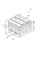
図1は、本実施形態のEL素子の要部を模式的に示す斜視図である。 FIG. 1 is a perspective view schematically showing a main part of the EL element of the present embodiment.
EL素子1は、基板2上に、下部電極3A、下部絶縁層4A、下部バッファ層6A、蛍光体層5(蛍光体薄膜)、上部バッファ層6B、上部絶縁層4B、及び上部電極3Bがこの順に積層されたものである。また、下部電極3A及び上部電極3Bには、交流電源7が接続されている。以下、まず、このEL素子1を構成する各層について説明する。
The EL element 1 includes a
(基板2)
基板2は、上部にEL素子1における各層を形成可能であり、また上方に形成された下部絶縁層4Aや下部バッファ層6Aを汚染するおそれがないものであれば特に限定されない。例えば、EL素子1の形成の際に行われるアニール処理におけるアニール温度に耐え得る耐熱性を有していることが好ましい。
(Substrate 2)
The
具体的には、好ましくは500℃以上、より好ましくは700℃以上、更に好ましくは800℃以上の耐熱温度又は融点を有するものが挙げられる。このような特性を有する基板用の材料としては、ガラス基板やセラミックス基板、セラミックス材料粉末をフィラーとしてガラス粉末を混合焼結させたガラスセラミックス基板、アルカリ土類結晶化成分を含む結晶化ガラス基板等が挙げられる。 Specifically, those having a heat-resistant temperature or melting point of preferably 500 ° C. or higher, more preferably 700 ° C. or higher, and still more preferably 800 ° C. or higher are mentioned. Examples of the material for the substrate having such characteristics include a glass substrate, a ceramic substrate, a glass ceramic substrate obtained by mixing and sintering glass powder using a ceramic material powder as a filler, and a crystallized glass substrate containing an alkaline earth crystallization component. Is mentioned.
なかでも、安価で入手が容易であり、しかも可視領域の光の透過性が高いという特性を有するガラス基板が好ましい。通常、EL素子の製造には、例えば700℃を超えるような高温条件でアニール処理を行う必要があった。ところが、ガラス基板はこのような高温条件では耐久性に劣るため、従来、EL素子における基板としての適用は困難であった。これに対し、本発明のEL素子においては、後述するように、このような高温でのアニール処理が必要ないため、上記ガラス基板の適用が可能となる。このようなガラス基板としては、例えばプラズマディスプレイパネル(PDP)に好適に用いられるガラス基板(ガラス歪点:550〜600℃)が挙げられる。 Among these, a glass substrate is preferable because it is inexpensive and easily available, and has high light transmittance in the visible region. Usually, for manufacturing an EL element, it is necessary to perform an annealing process under a high temperature condition exceeding 700 ° C., for example. However, since glass substrates are inferior in durability under such high temperature conditions, it has been difficult to apply them as substrates in EL devices. On the other hand, in the EL element of the present invention, as described later, since the annealing process at such a high temperature is not necessary, the glass substrate can be applied. Examples of such a glass substrate include a glass substrate (glass strain point: 550 to 600 ° C.) suitably used for a plasma display panel (PDP).
(下部電極3A)
下部電極3Aは、複数の帯状電極が一定間隔でストライプ状に一定方向に延在するように、基板2上に配設された構造を有している。この下部電極3Aは、所定の高導電性を発現するものであり、アニール処理の際の高温や酸化性雰囲気によって損傷を受け難いものであると好ましい。さらに、上方に形成される絶縁層4Aやバッファ層6A、蛍光体層5等との反応性が極力低いものであるとより好ましい。
(
The
具体的には、下部電極3Aを構成する材料としては、金属材料が好ましく、例えば、Au、Pt、Pd、Ir、Ag等の貴金属、Au−Pd、Au−Pt、Ag−Pd、Ag−Pt等の貴金属合金、Ag−Pd−Cu等の貴金属を主成分とし卑金属元素が添加された合金が好ましい例として挙げられる。これらの金属材料を用いることにより、高温又は酸化性雰囲気に対する耐性が充分に高められる。
Specifically, the material constituting the
(絶縁層4)
絶縁層4(下部絶縁層4A及び上部絶縁層4B)は、下部電極3A及び上部電極3Bの間に配置されており、バッファ層6A,6Bに挟持された蛍光体層5を挟むように設けられている。これらの絶縁層4の厚さは、5〜150nmであると好ましく、10〜100nmであるとより好ましい。
(Insulating layer 4)
The insulating layer 4 (lower insulating
このような絶縁層4としては2重絶縁型EL素子の絶縁層として用いられる絶縁材料から構成されるものであれば特に制限なく用いることができる。具体的には、酸化ケイ素(SiO2)、窒化ケイ素(Si3N4)、酸化タンタル(Ta2O5)、チタン酸ストロンチウム(SrTiO3)、酸化イットリウム(Y2O3)、ジルコニア(ZrO2)、シリコンオキシナイトライド(SiON)、アルミナ(Al2O3)等が挙げられる。 Such an insulating layer 4 can be used without particular limitation as long as it is made of an insulating material used as an insulating layer of a double insulation type EL element. Specifically, silicon oxide (SiO 2 ), silicon nitride (Si 3 N 4 ), tantalum oxide (Ta 2 O 5 ), strontium titanate (SrTiO 3 ), yttrium oxide (Y 2 O 3 ), zirconia (ZrO) 2 ), silicon oxynitride (SiON), alumina (Al 2 O 3 ) and the like.
(バッファ層6)
バッファ層6(下部バッファ層6A及び上部バッファ層6B)は、EL素子1において、下部電極3A及び下部電極3Bの間において一対の絶縁層4(下部絶縁層4A及び上部絶縁層4B)間に位置しており、蛍光体層5を挟むように配置されたものである。このバッファ層6は、キャリア注入層や拡散防止層として機能するものであり、例えば、蛍光体層5への電子注入を増強したり、また、EL素子の製造時にアニール処理を行う際に生じ易い、蛍光体層5への物質移動(マイグレーション)を抑制したりする効果を有している。
(Buffer layer 6)
The buffer layer 6 (lower buffer layer 6A and
このようなバッファ層6としては、例えば、ZnSから構成されるものが、上記効果を良好に生じ得ることから好適である。また、これらのバッファ層6の厚さは、上記効果を有効に発揮する観点から、30〜300nmであると好ましく、50〜200nmであるとより好ましい。 As such a buffer layer 6, for example, a layer composed of ZnS is preferable because the above effect can be favorably produced. Moreover, the thickness of these buffer layers 6 is preferably 30 to 300 nm, and more preferably 50 to 200 nm, from the viewpoint of effectively exhibiting the above effects.
(蛍光体層5)
蛍光体層5は、下部電極3Aと上部電極3Bとの間において下部絶縁層4A及び上部絶縁層4B間に位置しており、下部バッファ層6A及び上部バッファ層6Bに挟持された状態で配置されている。この蛍光体層5は、アルカリ金属、希土類金属及び遷移金属のうちのいずれか一種に属する金属元素、2族元素、13族元素、硫黄、ハロゲン、並びに発光中心材料を含有する蛍光体材料からなり、金属元素/2族元素の原子比が0.05〜5.00、好ましくは0.10〜2.80である蛍光体薄膜により構成されたものである。
(Phosphor layer 5)
The
この蛍光体層5の厚さは、50〜700nmであると好ましく、100〜500nmであるとより好ましく、100〜300nmであるとさらに好ましく、250nm程度であると特に好ましい。この厚さが50nm未満であると、発光輝度が不都合なほどに低下してしまうおそれがある。一方、700nmを越えると、発光を生じるために必要な最小の印加電圧である発光しきい電圧が過度に上昇し、実用的な動作電圧範囲での発光が見られなくなる場合がある。
The thickness of the
蛍光体層5を形成するための蛍光体材料に含まれる発光中心材料としては、通常、EL素子において発光中心元素として用いられる希土類元素又は遷移金属元素が適用できる。具体的には、希土類元素としては、Sc、Y、La、Ce、Pr、Nd、Gd、Tb、Ho、Er、Tm、Lu、Sm、Eu、Dy、Yb等が挙げられる。また、遷移金属元素としては、Mn、Pb、Bi、Cr等が挙げられる。なかでも、後述する蛍光体薄膜の状態で電界発光させた場合に青色発光を示すEu、Ce、Cu等が好ましく、特に高輝度且つ色純度の高い青色発光が得られるEuが好ましい。なお、上述の如く、蛍光体材料中には、アルカリ金属、希土類金属及び遷移金属のうちのいずれか一種に属する金属元素、2族元素及び13族元素が含有されているが、発光中心材料として含有される金属元素は、これらに用いた金属元素とは異なる種類の元素であることが好ましい。
As the luminescent center material contained in the phosphor material for forming the
また、蛍光体材料が含有しているアルカリ金属、希土類金属及び遷移金属のうちのいずれか一種に属する金属元素としては、アルカリ金属に属する金属元素が好ましく、特にLiが好ましい。さらに、2族元素としてはBaが好ましく、13族元素としてはAlが好ましい。さらにまた、蛍光体材料中のハロゲンとしては、Clが好ましい。
The metal element belonging to any one of the alkali metal, rare earth metal and transition metal contained in the phosphor material is preferably a metal element belonging to the alkali metal, particularly Li. Further, Ba is preferable as the
蛍光体層5を構成する蛍光体薄膜は、これらの元素を含有している蛍光体材料の原料組成物に対してアニール処理を行うことにより得られたものである。こうして形成された蛍光体薄膜においては、(金属元素/2族元素)の原子比が0.05〜5.00、好ましくは0.10〜2.80、より好ましくは0.20〜1.80、さらに好ましくは0.30〜1.40となっている。また、蛍光体薄膜が、このように蛍光体材料に対してアニール処理を行うことにより形成されたものである場合、そのアニール温度は、500℃以上700℃未満であると好ましく、500〜650℃であるとより好ましく、550〜600℃であると更に好ましい。
The phosphor thin film constituting the
このようにして形成された蛍光体層5は、基本的には、MII lMXIII mSnで表される母体材料及び発光中心材料を含む3元系の蛍光体となり、更に、この蛍光体中にアルカリ金属、希土類金属及び遷移金属のうちのいずれか一種に属する金属元素及びハロゲン原子が添加された構成を有するものとなる。なお、上記組成式において、MIIは2族元素、MXIIIは13族元素を示し、l、m及びnは、上記組成式で表される化合物が化学的に安定に存在できる組成となる整数である。
この蛍光体層5は、上述した組成に加えて、当該薄膜中にMA kMII lMXIII mSnで表される化合物を更に含有するものであってもよい。なお、かかる組成式において、MII、MXIII、l、m及びnは上記と同義であり、MAはアルカリ金属、希土類金属及び遷移金属のうちのいずれか一種に属する金属元素を示し、kは、上記組成式で表される化合物が化学的に安定に存在できる組成となる整数である。
The
このような構成を有する蛍光体層5(蛍光体薄膜)の好適な一例を以下に示す。例えば、蛍光体材料が、アルカリ金属、希土類金属及び遷移金属のうちのいずれか一種に属する金属元素としてLi、2族元素としてBa、13族元素としてAl、発光中心材料としてEu、ハロゲン原子としてClを含むものである場合、この蛍光体材料に対してアニール処理を行うことにより得られた蛍光体層5は、BaAl2S4で表される母体材料及び発光中心材料であるEuを基本的に含有している3元系の蛍光体に、Li及びClが更に添加された構成を有するものとなる。そして、これらの成分を含有している組成の好適な化学量論は、Li0.41Ba0.59Al2S4となる。
A preferred example of the phosphor layer 5 (phosphor thin film) having such a configuration is shown below. For example, the phosphor material is Li as a metal element belonging to any one of alkali metals, rare earth metals and transition metals, Ba as a
上述した構成の蛍光体層5は、BaAl2S4:Euで表される蛍光体により基本的に構成されるものであることから、高輝度且つ色純度のよい青色発光が可能となる。また、蛍光体層5を形成するための蛍光体材料の原料組成物は、Li及びClを含有していることから、この原料組成物を比較的低い温度(例えば500℃以上700℃未満)でアニール処理して蛍光体層5を形成させた場合であっても、得られた蛍光体層5は、十分に優れた輝度及び色純度を達成し得るものとなる。
Since the
(上部電極3B)
上部電極3Bは、複数の帯状電極が一定間隔でストライプ状に下部電極3Aの延在方向と直交する平面方向に延在するように発光層5上に配設されてなっている。この上部電極3Bは、EL素子1の図示上方から発光を取り出すように透明導電材料から構成されている。すなわち、このような上部電極3Bを備えるEL素子1は、素子の上方から発光を生じるトップエミッション型の構成を有している。
(
The
このような上部電極3を形成するための透明導電材料としては、In2O3、SnO2、ITO又はZnO−Alといった酸化物導電性材料等を用いることができる。また、その厚さは、0.2μm〜1μmであると好ましい。 As a transparent conductive material for forming such an upper electrode 3, an oxide conductive material such as In 2 O 3 , SnO 2 , ITO, or ZnO—Al can be used. The thickness is preferably 0.2 μm to 1 μm.
(EL素子1の製造方法)
次に、上述したEL素子1を製造する方法の実施形態について説明する。
(Manufacturing method of EL element 1)
Next, an embodiment of a method for manufacturing the above-described EL element 1 will be described.
まず、セラミックス基板、ガラスセラミックス基板又はガラス基板等から成る基板2を準備した後、この上にストライプ状に下部電極3Aを形成する。下部電極3Aの形成方法は特に制限されず、例えば、粉末金属ペースト、有機金属ペースト(レジネート金属ペースト)を用いた印刷法、或いは一般に用いられるエッチプロセス等を用いて形成できる。
First, after preparing a
次に、基板2上に、下部電極3Aを覆うように下部絶縁層4Aを形成する。下部絶縁層4Aの形成方法は特に限定されず、例えば、ゾルゲル法もしくは印刷焼成法などの公知の方法を挙げることができる。これらのなかで、印刷焼成法を用いる場合、下部電極3Aとなるペースト及び下部絶縁層4Aとなるペーストをそれぞれ印刷した後、これらを焼成することによって両層を形成させてもよい。さらに、このようにして下部絶縁層4Aを形成した後、蒸着法やスパッタリング法によって、例えばZnSからなる下部バッファ層6Aを形成させる。
Next, a lower insulating
続いて、下部バッファ層6Aが形成された積層体(被着体)における下部バッファ層6A上に、以下に示すようにして蛍光体層5を形成させる。以下、蛍光体層5の形成方法について詳細に説明する。
Subsequently, the
蛍光体層5は、上述した本発明の蛍光体材料からなる蛍光体薄膜により構成されるものであり、蛍光体材料を下部バッファ層6A上に堆積させて蛍光体材料層を形成した(堆積工程)後に、この蛍光体材料層に対してアニール処理を行う(アニール工程)方法により形成することができる。ここで、蛍光体材料層に対するアニール処理は、蛍光体材料層を下部バッファ層6A上に形成させた後すぐに行ってもよく、更に上方の層(例えば上部絶縁層4B等)を形成させた後に行ってもよい。
The
この方法において、堆積工程は、2族元素、13族元素、硫黄、及び発光中心材料を含む3元系の蛍光体を作製する際に通常用いられる蛍光体材料の原料組成物と、アルカリ金属、希土類金属及び遷移金属のうちのいずれか一種に属する金属元素のハロゲン化物とを、下部バッファ層6Aにおける蛍光体層5を形成させるべき所定の同一領域上に堆積させるようにして実施する。
In this method, the deposition step includes a raw material composition of a phosphor material that is normally used when producing a ternary phosphor containing a
このとき、原料組成物及びハロゲン化物の堆積は、蒸着法により行うことが好ましい。前者の原料組成物の蒸着は、原料組成物に含まれる各成分を全て含有している単一の蒸発源を用いて行うこともできるが、上述の如く、この原料組成物は3元系の蛍光体用の原料であることから、2種以上の蒸発源を用いる多元蒸着法により行うことが好ましい。このような多元蒸着法によって、好適な化学組成を有する蛍光体薄膜を形成することが容易となる。蒸着の際における蒸発源の加熱方法は特に限定されないが、これらの蒸発量をより厳密に制御できることから、電子ビーム(EB)による加熱を行うことがより好ましい。 At this time, the deposition of the raw material composition and the halide is preferably performed by an evaporation method. The former raw material composition can be vapor-deposited by using a single evaporation source containing all the components contained in the raw material composition. As described above, this raw material composition is a ternary system. Since it is a raw material for a phosphor, it is preferably carried out by a multi-source deposition method using two or more evaporation sources. By such a multi-source deposition method, it becomes easy to form a phosphor thin film having a suitable chemical composition. The method for heating the evaporation source during vapor deposition is not particularly limited, but it is more preferable to perform heating with an electron beam (EB) because the evaporation amount can be controlled more strictly.
ここで、原料組成物及びハロゲン化物の堆積は、下部バッファ層6Aの所定の同一領域に同時に行うようにして行ってもよく、また、一方の材料を堆積させた後に、他方の材料をその上に堆積させるようにして行ってもよい。前者の場合、具体的には、両方の材料を共蒸着させることが好ましい。こうすることで、蒸着と同時に両者が均一に分布するようになり、好適な場合には、基板上で両材料の反応が生じ、これにより上述したMA kMII lMXIII mSnで表される組成を有する化合物が生成する。一方、後者の方法を適用する場合には、両材料を堆積した後に行う蛍光体層5のアニール処理によって両材料の拡散が生じ、これにより両者が均一に分布することとなる。
Here, the deposition of the raw material composition and the halide may be performed simultaneously in a predetermined same region of the lower buffer layer 6A, and after depositing one material, the other material is deposited thereon. You may carry out so that it may deposit on. In the former case, specifically, it is preferable to co-deposit both materials. Thereby, now both are uniformly distributed at the same time evaporation and, where appropriate, the reaction of both materials occurs on the substrate, thereby at M A k M II l M XIII m S n described above A compound having the composition represented is produced. On the other hand, when the latter method is applied, both the materials are diffused by the annealing treatment of the
実施形態に係るEL素子1の製造方法(蛍光体薄膜の形成方法)においては、原料組成物及び添加材料の堆積は、原料組成物及びハロゲン化物を、下記式(1);
Hal/Lu=0.005〜0.125…(1)
で表される条件を満たすモル比で堆積させることが好ましい。なお、式中、Halはハロゲン化物のモル数、Luは原料組成物のモル数をそれぞれ示している。この、(Hal/Lu)のモル比は、0.01〜0.08とするとより好ましく、0.012〜0.062とするとより好ましい。このモル比がこれらの好適条件を満たすように原料組成物及びハロゲン化物を堆積させることによって、上述したような、蛍光体薄膜における(金属元素/2族元素)の原子比の好適な範囲(例えば、0.05〜5.00)を容易に達成できるようになる。
In the method for manufacturing the EL element 1 according to the embodiment (the method for forming the phosphor thin film), the deposition of the raw material composition and the additive material is performed by changing the raw material composition and halide into the following formula (1)
Hal / Lu = 0.005 to 0.125 (1)
It is preferable to deposit at a molar ratio satisfying the condition represented by In the formula, Hal represents the number of moles of halide, and Lu represents the number of moles of the raw material composition. The (Hal / Lu) molar ratio is more preferably 0.01 to 0.08, and more preferably 0.012 to 0.062. By depositing the raw material composition and the halide so that this molar ratio satisfies these preferable conditions, a suitable range of the atomic ratio of (metal element /
なお、原料組成物及びハロゲン化物の堆積量は、それぞれの蒸発源を加熱する程度を制御することにより調整することができる。例えばEBによる加熱を行う場合、それぞれの蒸発源に対するEBの照射時間を制御することによって両者の堆積量を適切に調節できる。 Note that the deposition amounts of the raw material composition and the halide can be adjusted by controlling the degree of heating of the respective evaporation sources. For example, when heating by EB is performed, the deposition amount of both can be appropriately adjusted by controlling the irradiation time of EB with respect to each evaporation source.
そして、蛍光体層5は、上述した堆積工程の後にアニール工程を行うことにより形成させる。この場合のアニール処理は、真空、N2もしくはArなどの還元性雰囲気、空気等の酸化性雰囲気、S蒸気、H2Sなどの雰囲気下、500℃以上700℃未満の温度条件で行うことが好ましい。かかるアニール処理によって、蛍光体層5の結晶性が向上するとともに、層中の組成が好適に調整される。
The
ここで、上述したアニール温度(500℃以上700℃未満)は、従来3元系の蛍光体を作製するために必要とされるアニール温度に比して低い温度である。通常、このようなアニール温度で処理を行った3元系の蛍光体は、実用的な電圧範囲では殆ど発光が見られないものとなっていた。これに対して、EL素子1における蛍光体層5は、上記本発明の蛍光体材料(蛍光体薄膜)からなるものであるため、500℃以上700℃未満という低いアニール温度で処理された場合であっても、十分に高い発光輝度を発揮し得るものとなる。
Here, the above-described annealing temperature (500 ° C. or higher and lower than 700 ° C.) is a lower temperature than the annealing temperature conventionally required for producing a ternary phosphor. Usually, a ternary phosphor processed at such an annealing temperature hardly emits light in a practical voltage range. On the other hand, since the
なお、例えば、通常の印加電圧よりも低い電圧範囲で高い輝度を得たい場合など、所望とするEL素子の特性によっては、これよりも高い温度でアニール処理を行っても構わない。この場合、基板2、電極3、絶縁層4及びバッファ層6の各層には、そのような高温にも耐え得る特性を有している材料を選択して用いることが望ましい。
Note that, for example, when it is desired to obtain high luminance in a voltage range lower than a normal applied voltage, the annealing treatment may be performed at a temperature higher than this depending on desired characteristics of the EL element. In this case, it is desirable to select and use materials having characteristics that can withstand such high temperatures for the
ここまで述べた蛍光体層5の形成方法の好適な一例を以下に示す。すなわち、まず、堆積工程において、蛍光体材料の原料組成物の蒸発源としてBaSにEuを添加したペレット、及び、粉状のAl2S3を用い、添加材料の蒸発源としてLiClを用い、これらを電子ビームにより共蒸着させて、蛍光体材料層を形成する。次いで、アニール工程において、蛍光体材料層に対して500℃以上700℃未満でアニール処理を行う。このようにして、上述した好適例である、BaAl2S4:Euからなる3元系の蛍光体に、Li及びClが更に添加された状態の蛍光体層5(蛍光体薄膜)が得られる。
A preferred example of the method for forming the
本発明によるEL素子1の製造においては、このようにして蛍光体層5を形成させた後、その上に、上部バッファ層6B及び上部絶縁層4Bを、上述した下部バッファ層6A及び下部絶縁層4Aの形成方法とそれぞれ同様にして形成させる。そして、上部絶縁層4B上に、下部電極3Aのストライプ方向に対して直交する方向に、上部電極3Bをストライプ状に形成してEL素子1を完成させる。上部電極3Bの形成方法としては、従来公知の方法が適用でき、例えば、蒸着法、スパッタリング法、CVD法、ゾルゲル法もしくは印刷焼成法が挙げられる。
In the manufacture of the EL device 1 according to the present invention, after the
なお、EL素子は、必ずしも上述したような構成に限定されるものではなく、本発明の主旨を逸脱しない範囲で他の形態を有していてもよい。 Note that the EL element is not necessarily limited to the above-described configuration, and may have other forms without departing from the gist of the present invention.
例えば、EL素子としての特性(輝度、色純度、素子寿命等)を向上させる観点から、EL素子は、上述した各層に加えて、他の層を更に備えるものであってもよい。具体的には、例えば、EL素子1における下部電極3Aと下部絶縁層4Aとの間に、厚膜絶縁体層が更に設けられていてもよい。こうすることで、蛍光体層5へのキャリア注入をさらに促進することや、蛍光体層5の平坦化を図ることができ、輝度等の特性がさらに向上する効果が得られる。このような厚膜絶縁体層は、セラミック材料を構成材料とするものであると好ましい。
For example, from the viewpoint of improving characteristics (luminance, color purity, element lifetime, etc.) as an EL element, the EL element may further include other layers in addition to the above-described layers. Specifically, for example, a thick film insulator layer may be further provided between the
セラミック材料としては、例えば、PbTiO3、PZT、PLZT等のペロブスカイト構造を持った(強)誘電体材料や、PMN(Pb(Mg1/3Nb2/3)O3)等に代表される複合ペロブスカイトリラクサー型強誘電体材料、Bi4Ti3O12、SrBi2Ta2O9等に代表されるビスマス層状化合物、(SrxBa1−x)Nb2O6、PbNb2O6等に代表されるタングステンブロンズ型強誘電体材料等が挙げられる。なお、「PZT」とは、Pb(ZrxTi1−x)O3を示す。 Examples of the ceramic material include (strong) dielectric materials having a perovskite structure such as PbTiO 3 , PZT, and PLZT, and composites represented by PMN (Pb (Mg 1/3 Nb 2/3 ) O 3 ). Perovskite relaxor-type ferroelectric material, bismuth layered compounds typified by Bi 4 Ti 3 O 12 , SrBi 2 Ta 2 O 9 etc., represented by (Sr x Ba 1-x ) Nb 2 O 6 , PbNb 2 O 6 etc. And tungsten bronze type ferroelectric materials. “PZT” indicates Pb (Zr x Ti 1-x ) O 3 .
この厚膜絶縁体層は、例えば、予めセラミック材料の粉末にバインダー、溶剤等を混合した厚膜ペーストを基板2上に下部電極3Aを覆うように塗布した後、乾燥させて厚膜グリーンとし、その後、この厚膜グリーンを焼成する方法や、ゾルゲル法、MOD(Metallo−organic decomposition)法等により形成することができる。
This thick film insulator layer is, for example, a thick film paste prepared by previously mixing a ceramic material powder with a binder, a solvent, etc. so as to cover the
さらに、本発明のEL素子は、電極、絶縁層、蛍光体層等の隣り合う各層の間に、密着性を上げるための層、応力を緩和するための層、反応を制御するための層など、各種中間層が設けられたものであってもよい。さらに、EL素子は、上述したトップエミッション型に限定されず、例えば、基板及び下部電極を透明材料から構成することによって、素子の下方から発光が見られるいわゆるボトムエミッション型のEL素子としてもよい。 Furthermore, the EL element of the present invention has a layer for improving adhesion, a layer for relaxing stress, a layer for controlling reaction, etc. between adjacent layers such as an electrode, an insulating layer, and a phosphor layer. Various intermediate layers may be provided. Furthermore, the EL element is not limited to the above-described top emission type, and may be a so-called bottom emission type EL element in which light emission is seen from below the element, for example, by forming the substrate and the lower electrode from a transparent material.
さらにまた、上記構成を有するEL素子1は、必ずしもバッファ層6を備えるものでなくてもよい。上述したように、従来の3元系の蛍光体を備えるEL素子においては、成膜時又はアニール時に高温で処理を行うと、EL素子の各層間で物質の移動(特に、蛍光体層への物資移動)が生じることがあった。こうなると、EL素子の輝度や素子寿命等の特性が低下する傾向にある。このため、従来は、このような物質移動を抑制するために、蛍光体層の両側に拡散防止層を設けることが多かった。これに対して、本発明によるEL素子は、その製造に際して従来よりも低いアニール温度を採用可能であることから、上述したような層間の物質移動が生じ難い。このため、物質移動を抑制する目的で形成させるバッファ層は省略することもできる。 Furthermore, the EL element 1 having the above-described configuration does not necessarily include the buffer layer 6. As described above, in an EL element including a conventional ternary phosphor, when a process is performed at a high temperature during film formation or annealing, the substance moves between each layer of the EL element (in particular, the phosphor layer). Material movement) may occur. In this case, characteristics such as luminance and element lifetime of the EL element tend to be deteriorated. For this reason, conventionally, in order to suppress such mass transfer, a diffusion preventing layer has often been provided on both sides of the phosphor layer. On the other hand, since the EL element according to the present invention can employ an annealing temperature lower than that in the prior art when manufacturing the EL element, the above-described material transfer between the layers hardly occurs. For this reason, the buffer layer formed for the purpose of suppressing mass transfer can be omitted.
なお、本実施形態においては、本発明の蛍光体材料及び蛍光体薄膜を用いた発光素子の好適な例として上述したEL素子を説明したが、これらが適用される発光素子は必ずしもEL素子に限定されず、例えばプラズマディスプレイパネル(PDP)等の蛍光体として応用することもできる。この場合も、蛍光体層を形成する際のアニール温度を低下させることができ、素子の構成及び製造工程を簡略化できる。 In the present embodiment, the above-described EL element has been described as a suitable example of the light-emitting element using the phosphor material and the phosphor thin film of the present invention. However, the light-emitting element to which these are applied is not necessarily limited to the EL element. For example, it can also be applied as a phosphor such as a plasma display panel (PDP). Also in this case, the annealing temperature at the time of forming the phosphor layer can be lowered, and the structure of the device and the manufacturing process can be simplified.
以下、本発明を実施例により更に詳細に説明するが、本発明はこれらの実施例に限定されるものではない。
[蛍光体材料のPL測定]
EXAMPLES Hereinafter, although an Example demonstrates this invention still in detail, this invention is not limited to these Examples.
[PL measurement of phosphor materials]
まず、本発明の蛍光体材料により得られる発光の程度を評価するため、蛍光体材料のPL(フォトルミネセンス)強度を測定した。
<PL測定用試料の作製>
First, in order to evaluate the degree of light emission obtained by the phosphor material of the present invention, the PL (photoluminescence) intensity of the phosphor material was measured.
<Preparation of PL measurement sample>
(実施例1)
Si基板上に、発光中心材料となるEuSを5.0mol%添加したBaS焼結体をEB電子銃で加熱して供給するとともに、Al2S3とMnCl2を抵抗加熱して供給し、硫化水素をフローしながら3源の蒸発レートを制御することによって、蛍光体材料を堆積させて、BaAl2S4:Euで表される蛍光体にMnCl2が添加された状態のPL測定用試料を形成した。得られたPL測定用試料に含まれるMn/Baの原子比をICP(高周波誘導結合プラズマ)及びXRF(蛍光X線)により測定したところ、0.40であった。
(Example 1)
A BaS sintered body to which 5.0 mol% of EuS as a light emission center material is added on a Si substrate is heated and supplied with an EB electron gun, and Al 2 S 3 and MnCl 2 are supplied with resistance heating, and sulfided. By controlling the evaporation rate of the three sources while flowing hydrogen, a phosphor material was deposited, and a sample for PL measurement in which MnCl 2 was added to the phosphor represented by BaAl 2 S 4 : Eu Formed. The atomic ratio of Mn / Ba contained in the obtained PL measurement sample was measured by ICP (high frequency inductively coupled plasma) and XRF (fluorescent X-ray), and was 0.40.
(実施例2〜4)
MnCl2に代えて、LiCl、LiF及びEuCl3を用いたこと以外は、実施例1と同様にしてPL測定用試料を作製した。LiCl、LiF及びEuCl3を用いた場合が、それぞれ実施例2、3及び4に該当する。なお、実施例2〜4のPL測定用試料におけるLi/Ba又はEu/Baの原子比は、それぞれ0.7、0.6及び0.05であった。
(Examples 2 to 4)
A sample for PL measurement was prepared in the same manner as in Example 1 except that LiCl, LiF and EuCl 3 were used instead of MnCl 2 . The cases using LiCl, LiF and EuCl 3 correspond to Examples 2, 3 and 4, respectively. The atomic ratios of Li / Ba or Eu / Ba in the PL measurement samples of Examples 2 to 4 were 0.7, 0.6, and 0.05, respectively.
(比較例1)
MnCl2を添加しなかったこと以外は実施例1と同様にしてPL測定用試料を作製した。
<PL測定>
(Comparative Example 1)
A sample for PL measurement was prepared in the same manner as in Example 1 except that MnCl 2 was not added.
<PL measurement>
実施例1〜4及び比較例1で得られたPL測定用試料に、励起光として発振波長325nmのHe−Cdレーザーを照射することによりPL測定を行った。得られた結果をまとめて図2及び図3に示す。図2は、各PL測定用試料で得られた波長に対する発光強度(相対値)を示すグラフである。また、図3は、図2におけるL4及びL5を拡大して示すグラフである。図2及び図3中、L1は実施例1、L2は実施例2、L3は実施例3、L4は実施例4、L5は比較例1のPL測定用試料を用いて得られた結果をそれぞれ示している。 PL measurement was performed by irradiating the PL measurement samples obtained in Examples 1 to 4 and Comparative Example 1 with He—Cd laser having an oscillation wavelength of 325 nm as excitation light. The obtained results are collectively shown in FIGS. FIG. 2 is a graph showing the emission intensity (relative value) with respect to the wavelength obtained for each PL measurement sample. FIG. 3 is an enlarged graph showing L4 and L5 in FIG. 2 and 3, L1 is Example 1, L2 is Example 2, L3 is Example 3, L4 is Example 4, and L5 is the result obtained using the PL measurement sample of Comparative Example 1. Show.
図2及び図3より、MnCl2、LiCl、LiF及びMnClが添加された実施例1〜4の蛍光体材料は、これらの添加を行わなかった比較例1の蛍光体材料に比して大きなPL強度を示すことが確認された。これにより、これらの添加は、蛍光体材料の発光強度を高め得ることが判明した。
[Li化合物の添加による発光輝度の変化の測定]
<EL素子の作製>
2 and 3, the phosphor materials of Examples 1 to 4 to which MnCl 2 , LiCl, LiF and MnCl were added were larger in PL than the phosphor material of Comparative Example 1 to which these additions were not performed. It was confirmed to show strength. Thus, it has been found that these additions can increase the emission intensity of the phosphor material.
[Measurement of change in luminance by addition of Li compound]
<Production of EL element>
(実施例5)
まず、基板2であるSiウェハ上に、Auを粉末金属ペースト状としたものをスクリーン印刷した後に焼成して下部電極3Aを形成した。次に、Al2O3ペレットを用いた蒸着法により、下部電極3A上にAl2O3からなる厚さ20nmの下部絶縁層4Aを形成した後、その上にZnSペレットを用いた蒸着法によってZnSからなる厚さ100nmの下部バッファ層6Aを形成した。
(Example 5)
First, on a Si wafer as the
次いで、Euを5.0モル%添加したBaS(BaS:Eu)からなるペレット、Al2S3からなるペレット、及び、LiClからなるペレットを入れたチャンバ内に、下部バッファ層6Aが形成された後の積層体(被着体)を入れた。その後、チャンバ内にH2Sガスを導入しながら各ペレットに電子ビーム(EB)を照射してこれらを同時に蒸発させ、各ペレットの材料を下部バッファ層6A上に共蒸着(堆積)させ、蛍光体層5となるべき厚さ250nmの蛍光体材料層を形成した。
Next, the lower buffer layer 6A was formed in a chamber containing a pellet made of BaS (BaS: Eu) to which 5.0 mol% of Eu was added, a pellet made of Al 2 S 3 and a pellet made of LiCl. The latter laminated body (adhered body) was put. Then, while introducing H 2 S gas into the chamber, each pellet is irradiated with an electron beam (EB) to evaporate them simultaneously, and the material of each pellet is co-evaporated (deposited) on the lower buffer layer 6A, and fluorescent light is emitted. A phosphor material layer having a thickness of 250 nm to be the
蛍光体材料層の形成後、その上にZnSペレットを用いた蒸着法によってZnSからなる厚さ100nmの上部バッファ層6Bを形成し、さらに、上部バッファ層6B上に、Al2O3ペレットを用いた蒸着法によりAl2O3からなる厚さ30nmの上部絶縁層4Bを形成した。その後、この上部絶縁層4B形成後の積層体に対して600℃でアニール処理を行うことで、蛍光体材料層から蛍光体層5を形成させた。そして、上部絶縁層4B上に、ITOターゲットを用いたRFマグネトロンスパッタリング法により厚さ400nmのITO透明電極(上部電極3B)を形成して、図1に示す構造のEL素子を得た。
After forming the phosphor material layer, an
なお、実施例5においては、蛍光体材料層を形成させる際のLiClの蒸着量(堆積量)を、BaS:Eu及びAi2S3の合計モル量に対して3.9mol%に設定した。そして、得られたEL素子における蛍光体層5中のLi及びBaの含有量を、ICP及びXRFにより測定したところ、Li/Baの原子比は0.69であった。
In Example 5, the deposition amount (deposition amount) of LiCl when forming the phosphor material layer was set to 3.9 mol% with respect to the total molar amount of BaS: Eu and Ai 2 S 3 . And when the content of Li and Ba in the
(実施例6)
LiClの蒸着量を11.7mol%としたこと以外は実施例5と同様にしてEL素子を製造した。得られたEL素子の蛍光体層5におけるLi/Baの原子比は2.13であった。
(Example 6)
An EL device was manufactured in the same manner as in Example 5 except that the deposition amount of LiCl was 11.7 mol%. The atomic ratio of Li / Ba in the
(実施例7)
LiClに代えてLiFを用いたこと以外は、実施例5と同様にしてEL素子を製造した。なお、実施例7においては、LiFの蒸着量を3.4mol%とした。また、得られたEL素子の蛍光体層5におけるLi/Baの原子比は、0.63であった。
(Example 7)
An EL device was manufactured in the same manner as in Example 5 except that LiF was used instead of LiCl. In Example 7, the deposition amount of LiF was 3.4 mol%. Moreover, the atomic ratio of Li / Ba in the
(比較例2)
LiClからなるペレットを用いなかったこと以外は実施例5と同様にしてEL素子を製造した。
<発光輝度の測定>
(Comparative Example 2)
An EL device was manufactured in the same manner as in Example 5 except that the pellet made of LiCl was not used.
<Measurement of emission luminance>
実施例5〜7及び比較例2で得られたEL素子を用い、以下に示す方法で各素子の発光輝度を測定した。すなわち、各素子における下部電極3A及び上部電極3Bにそれぞれリード線を接続した。そして、このリード線を介して両電極に、変調電圧:L60、駆動周波数:120Hz、印加電圧波形:パルス(パルス幅:100μs)、測定環境温度:25℃の条件で交流電圧を印加して各素子に発光を生じさせて、各素子に生じた発光の輝度(cd/m2)を測定した。得られた結果を図4にまとめて示した。
Using the EL elements obtained in Examples 5 to 7 and Comparative Example 2, the light emission luminance of each element was measured by the method described below. That is, lead wires were connected to the
図4は、実施例5〜7及び比較例2の各EL素子を用いて得られた印加電圧に対する発光輝度の変化を示すグラフである。図4中、L11は実施例7、L12は実施例5、L13は実施例6、L14は比較例2のEL素子を用いて得られたグラフをそれぞれ示している。 FIG. 4 is a graph showing changes in emission luminance with respect to applied voltage obtained using the EL elements of Examples 5 to 7 and Comparative Example 2. In FIG. 4, L11 is Example 7, L12 is Example 5, L13 is Example 6, and L14 is a graph obtained using the EL element of Comparative Example 2.
図4より、蛍光体層5中にLiCl又はLiFを添加した実施例5〜7のEL素子によれば、これらを添加しなかった比較例2のEL素子と比較して、極めて高い発光輝度が得られることが確認された。
[蛍光体層中のLi/Ba比による発光輝度の変化の測定]
<EL素子の作製>
From FIG. 4, according to the EL elements of Examples 5 to 7 in which LiCl or LiF was added to the
[Measurement of change in emission luminance due to Li / Ba ratio in phosphor layer]
<Production of EL element>
(実施例8)
下部バッファ層6A上に堆積させる、BaS:Eu及びAl2S3の合計モル数に対するLiClのモル数の比(Hal/Lu)を、0.005〜0.125の間で変化させて、種々のLi/Baの原子比を有する蛍光体層5を形成したこと以外は、実施例5と同様にして各種のEL素子を作成した。
<発光輝度の測定>
(Example 8)
The ratio of the number of moles of LiCl to the total number of moles of BaS: Eu and Al 2 S 3 deposited on the lower buffer layer 6A (Hal / Lu) is varied between 0.005 and 0.125, Various EL elements were prepared in the same manner as in Example 5 except that the
<Measurement of emission luminance>
得られた複数のEL素子のうち、Li/Baが原子比で、0.15、0.3、0.69、1.00、2.13、3.56であったものを選択し、これらのそれぞれに、変調電圧:L60、駆動周波数:120Hz、印加電圧波形:パルス(パルス幅:100μs)、測定環境温度:25℃の条件で交流電圧を印加して各素子に発光を生じさせて、各素子に生じた発光の輝度(cd/m2)を測定した。得られた結果を図5に示す。 Among the plurality of obtained EL elements, those having Li / Ba of 0.15, 0.3, 0.69, 1.00, 2.13, 3.56 in atomic ratio were selected, and these In each of the above, modulation voltage: L60, drive frequency: 120 Hz, applied voltage waveform: pulse (pulse width: 100 μs), measurement environment temperature: 25 ° C., an AC voltage is applied to cause each element to emit light, The luminance (cd / m 2 ) of light emission generated in each element was measured. The obtained results are shown in FIG.
図5は、蛍光体層におけるLi/Baの原子比に対する発光輝度の値を示すグラフである。図5中、上述した各EL素子の結果は丸で示されている。なお、図5中には、参考として実施例7及び比較例2のEL素子を同様の条件で発光させた場合の値がそれぞれ白抜き四角及び黒塗り四角で表されている。 FIG. 5 is a graph showing the value of the emission luminance with respect to the Li / Ba atomic ratio in the phosphor layer. In FIG. 5, the result of each EL element described above is indicated by a circle. In FIG. 5, for reference, values obtained when the EL elements of Example 7 and Comparative Example 2 were made to emit light under the same conditions are represented by white squares and black squares, respectively.
図5より、EL素子は、蛍光体層におけるLi/Baの比が0.15〜2.13である範囲で特に高い発光輝度を示すことが確認された。 From FIG. 5, it was confirmed that the EL element exhibited particularly high emission luminance in the range where the Li / Ba ratio in the phosphor layer was 0.15 to 2.13.
1…EL素子、2…基板、3A…下部電極、3B…上部電極、4A…下部絶縁層、4B…上部絶縁層、5…蛍光体層、6A…下部バッファ層、6B…上部バッファ層、7…交流電源。 DESCRIPTION OF SYMBOLS 1 ... EL element, 2 ... Board | substrate, 3A ... Lower electrode, 3B ... Upper electrode, 4A ... Lower insulating layer, 4B ... Upper insulating layer, 5 ... Phosphor layer, 6A ... Lower buffer layer, 6B ... Upper buffer layer, 7 …AC source.
Claims (9)
前記金属元素/前記2族元素の原子比が0.05〜5.00である、
ことを特徴とする蛍光体材料。 A metal element belonging to any one of alkali metal, rare earth metal and transition metal, group 2, element, group 13, element, sulfur, halogen, and luminescent center material,
The atomic ratio of the metal element / the group 2 element is 0.05 to 5.00,
A phosphor material characterized by that.
ことを特徴とする蛍光体薄膜。 A metal element belonging to any one of alkali metal, rare earth metal and transition metal, a group 2 element, a group 13 element, sulfur, halogen, and a phosphor material containing a luminescent center material, and the metal element / The atomic ratio of the Group 2 element is 0.05 to 5.00,
A phosphor thin film characterized by that.
前記一対の電極間に配置されており、アルカリ金属、希土類金属及び遷移金属のうちのいずれか一種に属する金属元素、2族元素、13族元素、硫黄、ハロゲン、並びに、発光中心材料を含む蛍光体材料からなり、且つ、
前記金属元素/前記2族元素の原子比が0.05〜5.00である蛍光体薄膜と、
を備えることを特徴とするEL素子。 A pair of electrodes facing each other;
Fluorescence which is disposed between the pair of electrodes and includes a metal element belonging to any one of alkali metal, rare earth metal and transition metal, a group 2 element, a group 13 element, sulfur, halogen, and an emission center material Made of body material, and
A phosphor thin film having an atomic ratio of the metal element / the group 2 element of 0.05 to 5.00;
An EL element comprising:
2族元素、13族元素、硫黄及び発光中心材料を含む蛍光体材料の原料組成物と、アルカリ金属、希土類金属及び遷移金属のうちのいずれか一種に属する金属元素のハロゲン化物とを、前記被着体の前記表面における同一領域上に堆積させて蛍光体材料層を形成する堆積工程と、
前記蛍光体材料層に対してアニール処理を行うアニール工程と、を有し、
前記堆積工程において、前記原料組成物及び前記ハロゲン化物を、下記式(1);
Hal/Lu=0.005〜0.125…(1)
[式中、Halはハロゲン化物のモル数、Luは原料組成物のモル数をそれぞれ示す。]
で表される条件を満たすモル比で堆積させる、
ことを特徴とする蛍光体薄膜の形成方法。 A method of forming a phosphor thin film on the surface of an adherend,
A raw material composition of a phosphor material containing a group 2 element, a group 13 element, sulfur and a luminescent center material, and a halide of a metal element belonging to any one of alkali metals, rare earth metals and transition metals A deposition step of depositing on the same region of the surface of the adherend to form a phosphor material layer;
An annealing step for performing an annealing process on the phosphor material layer,
In the deposition step, the raw material composition and the halide are represented by the following formula (1):
Hal / Lu = 0.005 to 0.125 (1)
[In the formula, Hal represents the number of moles of the halide, and Lu represents the number of moles of the raw material composition. ]
Deposited at a molar ratio that satisfies the condition represented by
A method for forming a phosphor thin film.
Priority Applications (1)
| Application Number | Priority Date | Filing Date | Title |
|---|---|---|---|
| JP2004106934A JP2005290196A (en) | 2004-03-31 | 2004-03-31 | Phosphor material, phosphor thin film and its manufacturing method, light-emitting element, and el device |
Applications Claiming Priority (1)
| Application Number | Priority Date | Filing Date | Title |
|---|---|---|---|
| JP2004106934A JP2005290196A (en) | 2004-03-31 | 2004-03-31 | Phosphor material, phosphor thin film and its manufacturing method, light-emitting element, and el device |
Publications (1)
| Publication Number | Publication Date |
|---|---|
| JP2005290196A true JP2005290196A (en) | 2005-10-20 |
Family
ID=35323499
Family Applications (1)
| Application Number | Title | Priority Date | Filing Date |
|---|---|---|---|
| JP2004106934A Pending JP2005290196A (en) | 2004-03-31 | 2004-03-31 | Phosphor material, phosphor thin film and its manufacturing method, light-emitting element, and el device |
Country Status (1)
| Country | Link |
|---|---|
| JP (1) | JP2005290196A (en) |
Cited By (2)
| Publication number | Priority date | Publication date | Assignee | Title |
|---|---|---|---|---|
| JP2008251336A (en) * | 2007-03-30 | 2008-10-16 | Kuraray Luminas Co Ltd | Thin film type inorganic el element |
| JP2022032021A (en) * | 2020-08-10 | 2022-02-24 | インダストリー アカデミー コーオペレーション ファウンデーション オブ セジョン ユニバーシティー | Sulfide phosphor and light-emitting device comprising the same |
-
2004
- 2004-03-31 JP JP2004106934A patent/JP2005290196A/en active Pending
Cited By (2)
| Publication number | Priority date | Publication date | Assignee | Title |
|---|---|---|---|---|
| JP2008251336A (en) * | 2007-03-30 | 2008-10-16 | Kuraray Luminas Co Ltd | Thin film type inorganic el element |
| JP2022032021A (en) * | 2020-08-10 | 2022-02-24 | インダストリー アカデミー コーオペレーション ファウンデーション オブ セジョン ユニバーシティー | Sulfide phosphor and light-emitting device comprising the same |
Similar Documents
| Publication | Publication Date | Title |
|---|---|---|
| JP3704068B2 (en) | EL panel | |
| US6939482B2 (en) | Phosphor thin film, manufacturing method of the same, and electroluminescent panel | |
| JP3704057B2 (en) | Phosphor thin film and method for manufacturing the same, and EL panel | |
| JP2003238953A (en) | Phosphor and el panel | |
| KR100487895B1 (en) | Phosphor Thin Film, Its Production Method and EL Panel | |
| JP4230363B2 (en) | Phosphor thin film, manufacturing method thereof, and EL panel | |
| US8466615B2 (en) | EL functional film and EL element | |
| KR100497523B1 (en) | Phosphor Thin Film, Its Production Method, and EL Panel | |
| JP4263001B2 (en) | Sputtering target | |
| JP3472236B2 (en) | Phosphor thin film, manufacturing method thereof and EL panel | |
| JP4212300B2 (en) | EL phosphor laminated thin film and EL element | |
| JP4230164B2 (en) | Phosphor thin film, manufacturing method thereof, and EL panel | |
| KR100405185B1 (en) | Fluorescent Thin Film, Preparation Method and EL Panel | |
| JP2005290196A (en) | Phosphor material, phosphor thin film and its manufacturing method, light-emitting element, and el device | |
| JP4206221B2 (en) | EL phosphor laminated thin film and EL element | |
| JP2003055651A (en) | Phosphor thin film and el panel | |
| JP4831939B2 (en) | Luminescent thin film and light emitting element | |
| KR100496400B1 (en) | Phosphor Thin Film, Its Production Method, and EL Panel | |
| JP2002110351A (en) | Laminated phosphor and el panel | |
| JP2003272848A (en) | Manufacturing method of phosphor thin film and el panel | |
| JP2002201468A (en) | Phosphor thin film, its preparation process and el panel | |
| JP2001250681A (en) | Manufacturing method of sulfide light emission layer and manufacturing apparatus | |
| JP2003301170A (en) | Phosphor thin film, production process therefor, and el panel | |
| JP2003003161A (en) | Phosphor thin film, method for producing the same and el panel | |
| JP2003201471A (en) | Fluorescent thin film and el panel |
Legal Events
| Date | Code | Title | Description |
|---|---|---|---|
| A02 | Decision of refusal |
Free format text: JAPANESE INTERMEDIATE CODE: A02 Effective date: 20060104 |