JP2005292796A - Image blur correction device - Google Patents
Image blur correction device Download PDFInfo
- Publication number
- JP2005292796A JP2005292796A JP2005038720A JP2005038720A JP2005292796A JP 2005292796 A JP2005292796 A JP 2005292796A JP 2005038720 A JP2005038720 A JP 2005038720A JP 2005038720 A JP2005038720 A JP 2005038720A JP 2005292796 A JP2005292796 A JP 2005292796A
- Authority
- JP
- Japan
- Prior art keywords
- magnetic field
- field change
- detection
- horizontal
- current value
- Prior art date
- Legal status (The legal status is an assumption and is not a legal conclusion. Google has not performed a legal analysis and makes no representation as to the accuracy of the status listed.)
- Granted
Links
Images


Landscapes
- Adjustment Of Camera Lenses (AREA)
- Studio Devices (AREA)
Abstract
【課題】 像ブレ補正装置の磁界変化検出素子を使用した位置検出において位置検出に関する出力値の調整を電気的調整のみで行う装置を提供する。
【解決手段】 第1、第2検出位置信号が入力されA/D変換後に可動部の第1、第2方向の位置を演算し、且つ可動部、固定部、ホール素子信号処理回路部を制御するCPUを備える。水平方向ホール素子の入力端子を流れる電流値を変化させて第1検出位置信号をA/D変換する際の第1の検出分解能を上げる第1初期調整によって求められた最適水平方向ホール素子電流値を、可動部の位置検出時に水平方向ホール素子の入力端子に流し、鉛直方向ホール素子の入力端子を流れる電流値を変化させて第2検出位置信号をA/D変換する際の第2の検出分解能を上げる第2初期調整によって求められた最適鉛直方向ホール素子電流値を、可動部の位置検出時に鉛直方向ホール素子の入力端子に流す。
【選択図】 図12PROBLEM TO BE SOLVED: To provide an apparatus for adjusting an output value related to position detection only by electrical adjustment in position detection using a magnetic field change detection element of an image blur correction apparatus.
SOLUTION: After the first and second detection position signals are inputted and A / D converted, the positions of the movable part in the first and second directions are calculated, and the movable part, the fixed part, and the Hall element signal processing circuit part are controlled. CPU is provided. The optimum horizontal hall element current value obtained by the first initial adjustment for increasing the first detection resolution when the first detection position signal is A / D converted by changing the current value flowing through the input terminal of the horizontal hall element. Is sent to the input terminal of the horizontal hall element when detecting the position of the movable part, and the second detection position signal is A / D converted by changing the current value flowing through the input terminal of the vertical hall element. The optimum vertical hall element current value obtained by the second initial adjustment for increasing the resolution is supplied to the input terminal of the vertical hall element when the position of the movable portion is detected.
[Selection] FIG.
Description
本発明は、撮像装置における像ブレ補正装置に関し、特に像ブレ補正のために移動した撮像素子などの可動部の位置検出装置に関する。 The present invention relates to an image blur correction apparatus in an imaging apparatus, and more particularly to a position detection apparatus for a movable part such as an image sensor that has moved for image blur correction.
従来、カメラなどの撮像装置において撮像中に生じた手ブレ量に応じて、像ブレ補正レンズまたは撮像素子を光軸と垂直な平面上を移動させることにより結像面上での像ブレを抑制する像ブレ補正装置が提案されている。 Conventionally, image blurring on the image plane is suppressed by moving the image blur correction lens or image sensor on a plane perpendicular to the optical axis in accordance with the amount of camera shake that occurs during imaging in an imaging device such as a camera. An image blur correction device has been proposed.
特許文献1は、像ブレ補正レンズを含む可動部について磁石とコイルによって移動を行い、その移動前後の位置検出はホール素子と磁石によって行う装置を開示する。
しかし、特許文献1の装置のようなホール素子などの磁界変化検出素子を使用した可動部の位置検出において、磁界変化検出素子からの出力信号から求めた位置検出に関する出力値の調整は一般的に、信号処理回路の増幅率(アンプゲイン)により行われていた。そのため、信号処理回路にある抵抗値を変化させる機械的調整が必要であり、生産性に問題があった。
However, in the position detection of a movable part using a magnetic field change detection element such as a Hall element as in the apparatus of
したがって本発明の目的は、像ブレ補正装置の磁界変化検出素子を使用した位置検出において位置検出に関する出力値の調整を電気的調整のみで行う装置を提供することである。 Accordingly, an object of the present invention is to provide an apparatus for adjusting an output value related to position detection only by electrical adjustment in position detection using a magnetic field change detection element of an image blur correction apparatus.
本発明に係る撮像装置の像ブレ補正装置は、撮像素子または像ブレ補正レンズのいずれか一方を有し、撮影レンズの光軸に直交する第1方向と、光軸及び第1方向に直交する第2方向に移動可能な可動部と、可動部を第1、第2方向に移動自在に支持する固定部とを備え、可動部または固定部のいずれか一方は、可動部の第1方向の位置検出に使用される水平方向磁界変化検出素子と、可動部の第2方向の位置検出に使用される鉛直方向磁界変化検出素子とを有する磁界変化検出部を有し、可動部または固定部のいずれか他方は、可動部の第1、第2方向の位置検出に使用される位置検出用磁石を、磁界変化検出部に対向する位置に有し、水平方向磁界変化検出素子の出力信号から可動部の位置検出のため第1方向の位置を特定する第1検出位置信号を出力し、鉛直方向磁界変化検出素子の出力信号から可動部の位置検出のため第2方向の位置を特定する第2検出位置信号を出力する信号処理部と、第1、第2検出位置信号が入力されA/D変換後に可動部の第1、第2方向の位置を演算し、且つ可動部、固定部、信号処理部を制御する制御手段とを備え、水平方向磁界変化検出素子の入力端子を流れる電流値を変化させて第1検出位置信号をA/D変換する際の第1の検出分解能を上げる第1初期調整によって求められた最適水平方向磁界変化検出素子電流値を、可動部の位置検出時に水平方向磁界変化検出素子の入力端子に流し、鉛直方向磁界変化検出素子の入力端子を流れる電流値を変化させて第2検出位置信号をA/D変換する際の第2の検出分解能を上げる第2初期調整によって求められた最適鉛直方向磁界変化検出素子電流値を、可動部の位置検出時に鉛直方向磁界変化検出素子の入力端子に流す。 An image blur correction apparatus for an image pickup apparatus according to the present invention includes either an image pickup element or an image blur correction lens, and is orthogonal to a first direction orthogonal to the optical axis of the photographing lens, and to the optical axis and the first direction. A movable portion movable in the second direction, and a fixed portion that supports the movable portion in a movable manner in the first and second directions, and either the movable portion or the fixed portion is arranged in the first direction of the movable portion. A magnetic field change detection unit having a horizontal direction magnetic field change detection element used for position detection and a vertical direction magnetic field change detection element used for position detection in the second direction of the movable unit; The other has a position detection magnet used for detecting the position of the movable part in the first and second directions at a position facing the magnetic field change detection part, and is movable from the output signal of the horizontal magnetic field change detection element. 1st detection which specifies the position of the 1st direction for position detection A signal processing unit for outputting a position signal and outputting a second detection position signal for specifying the position in the second direction for detecting the position of the movable part from the output signal of the vertical direction magnetic field change detection element; and first and second detections A horizontal direction magnetic field change detecting element comprising: a control means for calculating a position of the movable portion in the first and second directions after the position signal is inputted and A / D converted, and controlling the movable portion, the fixed portion, and the signal processing portion; The optimum horizontal direction magnetic field change detection element current value obtained by the first initial adjustment for increasing the first detection resolution when the first detection position signal is A / D converted by changing the current value flowing through the input terminal of When the position of the movable portion is detected, a second current is passed through the input terminal of the horizontal direction magnetic field change detecting element and the current value flowing through the input terminal of the vertical direction magnetic field change detecting element is changed to A / D convert the second detected position signal. Second initial adjustment to increase detection resolution Accordingly the optimum vertical magnetic field change detection element current value determined, flow to the input terminals of the vertical magnetic field change detection element for position detection of the movable portion.
これにより、A/D変換を行う際の検出分解能を上げるための初期調整は磁界変化検出素子の入力端子に流す電流値を変化させる電気的調整のみで可能になり、生産性が向上する。 Thereby, initial adjustment for increasing the detection resolution at the time of A / D conversion can be performed only by electrical adjustment for changing the value of the current flowing through the input terminal of the magnetic field change detection element, and productivity is improved.
好ましくは、第1初期調整は、可動部が第1方向の一方の端点にあって第1検出位置信号の出力値がA/D変換が可能な範囲内で最大となる時の水平方向磁界変化検出素子の入力端子を流れる第1水平方向磁界変化検出素子電流値と、可動部が第1方向の他方の端点にあって第1検出位置信号の出力値がA/D変換が可能な範囲内で最小となる時の水平方向磁界変化検出素子の入力端子を流れる第2水平方向磁界変化検出素子電流値とを求め、第1、第2水平方向磁界変化検出素子電流値のうち小さい方の値を最適水平方向磁界変化検出素子電流値とし、第2初期調整は、可動部が第2方向の一方の端点にあって第2検出位置信号の出力値がA/D変換が可能な範囲内で最大となる時の鉛直方向磁界変化検出素子の入力端子を流れる第1鉛直方向磁界変化検出素子電流値と、可動部が第2方向の他方の端点にあって第2検出位置信号の出力値がA/D変換が可能な範囲内で最小となる時の鉛直方向磁界変化検出素子の入力端子を流れる第2鉛直方向磁界変化検出素子電流値とを求め、第1、第2鉛直方向磁界変化検出素子電流値のうち小さい方の値を最適鉛直方向磁界変化検出素子電流値とする。 Preferably, the first initial adjustment is performed by changing the horizontal magnetic field when the movable part is at one end point in the first direction and the output value of the first detection position signal is maximum within a range where A / D conversion is possible. The first horizontal direction magnetic field change detection element current value flowing through the input terminal of the detection element and the output value of the first detection position signal within the range in which A / D conversion is possible because the movable part is at the other end point in the first direction. The second horizontal magnetic field change detecting element current value flowing through the input terminal of the horizontal magnetic field change detecting element at the time of the minimum is obtained, and the smaller one of the first and second horizontal magnetic field change detecting element current values is obtained. Is the optimum horizontal magnetic field change detection element current value, and the second initial adjustment is performed within a range where the movable part is at one end point in the second direction and the output value of the second detection position signal can be A / D converted. The first vertical that flows through the input terminal of the vertical direction magnetic field change detecting element at the maximum Directional magnetic field change detection element current value and vertical magnetic field change when the movable part is at the other end point in the second direction and the output value of the second detection position signal is minimum within a range where A / D conversion is possible The second vertical magnetic field change detection element current value flowing through the input terminal of the detection element is obtained, and the smaller one of the first and second vertical magnetic field change detection element current values is determined as the optimum vertical magnetic field change detection element current value. And
また、好ましくは、固定部は磁界変化検出部を有し、可動部は位置検出用磁石を有し、磁界変化検出部は、水平方向磁界変化検出素子としてそれぞれの入力端子が直列に接続される第1、第2水平方向磁界変化検出素子を有し、鉛直方向磁界変化検出素子としてそれぞれの入力端子が直列に接続される第1、第2鉛直方向磁界変化検出素子を有する。これにより、2つの磁界変化検出素子におけるそれぞれの出力端子間の電位差の差異を求めることで直線的な変化量を使って精度の高い位置検出を行うことが可能になる。 Preferably, the fixed part has a magnetic field change detection part, the movable part has a position detection magnet, and each input terminal is connected in series as a horizontal direction magnetic field change detection element. It has 1st, 2nd horizontal direction magnetic field change detection elements, and has 1st, 2nd vertical direction magnetic field change detection elements to which each input terminal is connected in series as a vertical direction magnetic field change detection element. Accordingly, it is possible to perform highly accurate position detection using a linear change amount by obtaining a difference in potential difference between the output terminals of the two magnetic field change detection elements.
さらに好ましくは、位置検出用磁石は、磁界変化検出部に対向する面が第1、第2方向のいずれか一方と平行な線で形成される正方形であり且つ光軸と平行な第3方向にN極とS極が並べられて可動部に取り付けられる。これにより、1つの磁石で水平方向磁界変化検出素子を使った第1方向の位置検出、及び鉛直方向磁界変化検出素子を使った第2方向の位置検出を行うことが可能になる。 More preferably, the position detecting magnet is a square formed by a line parallel to one of the first and second directions and a third direction parallel to the optical axis. N pole and S pole are arranged and attached to the movable part. Accordingly, it is possible to perform position detection in the first direction using the horizontal magnetic field change detection element and position detection in the second direction using the vertical magnetic field change detection element with one magnet.
さらに好ましくは、可動部の移動によって光軸が撮像素子または像ブレ補正レンズのいずれか一方の中心近傍を通る位置関係にある時に、第1、第2水平方向磁界変化検出素子の第2方向の位置は、いずれも正方形の第2方向の中間近傍に対向し、第1方向の位置は、それぞれ正方形の第1方向の両端部近傍に対向し、第1、第2鉛直方向磁界変化検出素子の第1方向の位置は、いずれも正方形の第1方向の中間近傍に対向し、第2方向の位置は、それぞれ正方形の第2方向の両端部近傍に対向する。これにより、位置検出用磁石の正方形の大きさを最大限活用して位置検出を行うことが可能になる。 More preferably, when the optical axis is in a positional relationship passing near the center of one of the image sensor and the image blur correction lens due to the movement of the movable part, the first and second horizontal direction magnetic field change detection elements in the second direction The positions of the first and second vertical direction magnetic field change detecting elements are both opposed to the vicinity of the middle of the second direction of the square, and the positions of the first direction are opposed to the vicinity of both ends of the first direction of the square. Each position in the first direction faces the vicinity of the middle of the first direction of the square, and each position in the second direction faces the vicinity of both ends of the second direction of the square. As a result, position detection can be performed by making maximum use of the square size of the position detection magnet.
また、好ましくは、磁界変化検出部は、2軸ホール素子であり、第1、第2水平方向磁界変化検出素子、第1、第2鉛直方向磁界変化検出素子は、いずれもホール素子である。 Preferably, the magnetic field change detection unit is a biaxial Hall element, and the first and second horizontal magnetic field change detection elements and the first and second vertical magnetic field change detection elements are all Hall elements.
また、好ましくは、可動部は磁界変化検出部を有し、固定部は位置検出用磁石を有し、磁界変化検出部は、水平方向磁界変化検出素子と鉛直方向磁界変化検出素子を1つずつ有し、位置検出用磁石は、水平方向磁界変化検出素子と対向する位置に取り付けられて第1方向の位置検出に使用される第1位置検出用磁石と、鉛直方向磁界変化検出素子と対向する位置に取り付けられて第2方向の位置検出に使用される第2位置検出用磁石とから構成される。これにより、1つの磁界変化検出素子における出力端子間の電位差を求め且つ可動部に取り付けられる磁界変化検出素子を使って位置検出を行うことが可能になる。 Preferably, the movable part has a magnetic field change detection part, the fixed part has a position detecting magnet, and the magnetic field change detection part has one horizontal magnetic field change detection element and one vertical magnetic field change detection element. A position detecting magnet that is attached to a position facing the horizontal magnetic field change detecting element and that is used for position detection in the first direction; and a vertical magnetic field change detecting element. And a second position detection magnet attached to the position and used for position detection in the second direction. As a result, the potential difference between the output terminals of one magnetic field change detecting element can be obtained, and position detection can be performed using the magnetic field change detecting element attached to the movable part.
さらに、好ましくは、可動部は、可動部を第1方向に移動させるために使用される第1駆動用コイルと、可動部を第2方向に移動させるために使用される第2駆動用コイルとを有し、第1位置検出用磁石は、可動部を第1方向に移動させるためにも使用され、第2位置検出用磁石は、可動部を第2方向に移動させるためにも使用される。これにより、可動部の位置検出用磁石を共用して可動部の駆動用に使用することが可能になる。 Further preferably, the movable part includes a first drive coil used for moving the movable part in the first direction, and a second drive coil used for moving the movable part in the second direction. The first position detection magnet is also used to move the movable part in the first direction, and the second position detection magnet is also used to move the movable part in the second direction. . Thereby, it becomes possible to share the position detecting magnet of the movable part and use it for driving the movable part.
また、好ましくは、磁界変化検出部は、1軸ホール素子であり、水平方向磁界変化検出素子、鉛直方向磁界変化検出素子は、いずれもホール素子である。 Preferably, the magnetic field change detection unit is a uniaxial Hall element, and both the horizontal magnetic field change detection element and the vertical magnetic field change detection element are Hall elements.
また、好ましくは、可動部は位置検出用磁石を有し、固定部は前記磁界変化検出部を有し、磁界変化検出部は、水平方向磁界変化検出素子と鉛直方向磁界変化検出素子を1つずつ有し、位置検出用磁石は、水平方向磁界変化検出素子と対向し第1方向にN極とS極が並べられて可動部に取り付けられる第1位置検出用磁石と、鉛直方向磁界変化検出素子と対向し第2方向にN極とS極が並べられて可動部に取り付けられる第2位置検出用磁石とを有する。これにより、1つの磁界変化検出素子における出力端子間の電位差を求め且つ固定部に取り付けられる磁界変化検出素子を使って位置検出を行うことが可能になる。 Preferably, the movable part has a position detection magnet, the fixed part has the magnetic field change detection part, and the magnetic field change detection part has one horizontal magnetic field change detection element and one vertical magnetic field change detection element. Each of the position detection magnets has a first position detection magnet which is opposed to the horizontal direction magnetic field change detection element and has a north pole and a south pole arranged in the first direction and attached to the movable portion, and a vertical direction magnetic field change detection. There is a second position detection magnet attached to the movable part, with the N and S poles arranged in the second direction so as to face the element. As a result, the potential difference between the output terminals of one magnetic field change detecting element can be obtained, and the position can be detected using the magnetic field change detecting element attached to the fixed portion.
また、好ましくは、制御手段と接続され、最適水平方向磁界変化検出素子電流値、及び最適鉛直方向磁界変化検出素子電流値を記録し、電源がオフ状態にされても内容が消去されないメモリ部を備える。これにより、一度最適水平方向磁界変化検出素子電流値、最適鉛直方向磁界変化検出素子電流値を設定すれば、電源をオフ状態にしたあとも、再度初期調整を行うことなく、最適水平方向磁界変化検出素子電流値、最適鉛直方向磁界変化検出素子電流値を使って水平方向磁界変化検出素子及び鉛直方向磁界変化検出素子の入力回路に電流を流すことが可能になる。 Preferably, the memory unit is connected to the control unit, records the optimum horizontal magnetic field change detection element current value and the optimum vertical magnetic field change detection element current value, and does not erase the contents even when the power is turned off. Prepare. As a result, once the optimal horizontal magnetic field change detection element current value and optimal vertical magnetic field change detection element current value are set, the optimal horizontal magnetic field change can be made without initial adjustment again after the power is turned off. Using the detection element current value and the optimum vertical magnetic field change detection element current value, it is possible to pass a current through the input circuit of the horizontal magnetic field change detection element and the vertical magnetic field change detection element.
また、好ましくは、可動部の移動によって光軸が撮像素子または像ブレ補正レンズのいずれか一方の中心近傍を通る位置関係にある時に、第1、第2方向ともに可動部が移動範囲の中心に位置する。これにより、撮像素子の撮像範囲または像ブレ補正レンズの有効範囲を最大限活用して像ブレ補正を行うことが可能になる。 Preferably, when the movable part moves so that the optical axis passes through the vicinity of the center of either the image sensor or the image blur correction lens, the movable part is at the center of the moving range in both the first and second directions. To position. As a result, it is possible to perform image blur correction by making maximum use of the imaging range of the image sensor or the effective range of the image blur correction lens.
また、好ましくは、像ブレ補正装置における初期調整の方法は、可動部を第1方向の一方の端点に移動させ、第1検出位置信号の出力値がA/D変換が可能な範囲内で最大となる時の水平方向磁界変化検出素子の入力端子に流れる第1水平方向磁界変化検出素子電流値を求める第1ステップと、可動部を第1方向の他方の端点に移動させ、第1検出位置信号の出力値がA/D変換が可能な範囲内で最小となる時の水平方向磁界変化検出素子に流れる第2水平方向磁界変化検出素子電流値を求める第2ステップと、可動部を第2方向の一方の端点に移動させ、第2検出位置信号の出力値がA/D変換が可能な範囲内で最大となる時の鉛直方向磁界変化検出素子に流れる第1鉛直方向磁界変化検出素子電流値を求める第3ステップと、可動部を第2方向の他方の端点に移動させ、第2検出位置信号の出力値がA/D変換が可能な範囲内で最小となる時の鉛直方向磁界変化検出素子に流れる第2鉛直方向磁界変化検出素子電流値を求める第4ステップと、第1、第2水平方向磁界変化検出素子電流値の中で小さい方の値を最適水平方向磁界変化検出素子電流値とし、第1、第2鉛直方向磁界変化検出素子電流値の中で小さい方の値を最適鉛直方向磁界変化検出素子電流値とする第5ステップとを備える。 Preferably, in the method of initial adjustment in the image blur correction apparatus, the movable portion is moved to one end point in the first direction, and the output value of the first detection position signal is maximized within a range where A / D conversion is possible. A first step of obtaining a current value of the first horizontal magnetic field change detecting element flowing through the input terminal of the horizontal magnetic field change detecting element at the time, and moving the movable portion to the other end point in the first direction, A second step of obtaining a current value of a second horizontal magnetic field change detecting element flowing in the horizontal magnetic field change detecting element when the output value of the signal is minimum within a range where A / D conversion is possible; The first vertical magnetic field change detection element current that flows through the vertical magnetic field change detection element when the output value of the second detection position signal is maximized within a range where A / D conversion is possible. The third step to find the value and the movable part The second vertical magnetic field change detection element current flowing in the vertical magnetic field change detection element when the output value of the second detection position signal is minimized within the range where A / D conversion is possible. The fourth step of obtaining the value, and the smaller one of the first and second horizontal magnetic field change detecting element current values is set as the optimum horizontal magnetic field change detecting element current value, and the first and second vertical magnetic field change detections are performed. And a fifth step of setting the smaller one of the element current values as the optimum vertical magnetic field change detection element current value.
さらに好ましくは、最適水平方向磁界変化検出素子電流値、及び最適鉛直方向磁界変化検出素子電流値を、電源がオフ状態にされても内容が消去されないメモリ部に記録する第6ステップを備える。 More preferably, a sixth step of recording the optimum horizontal direction magnetic field change detection element current value and the optimum vertical direction magnetic field change detection element current value in a memory unit whose contents are not erased even when the power is turned off is provided.
また、本発明に係る他の撮像装置の像ブレ補正装置は、撮像素子または像ブレ補正レンズのいずれか一方を有し、撮影レンズの光軸に直交する平面上を移動可能な可動部と、可動部を平面上に移動自在に支持する固定部とを備え、可動部または固定部のいずれか一方は、可動部の位置検出に使用される磁界変化検出部を有し、磁界変化検出部の出力信号から可動部の位置検出のため位置を特定する検出位置信号を出力する信号処理部と、磁界変化検出部を駆動する制御信号を変化させて検出位置信号の出力値を調整する初期調整によって求められた最適な制御信号で、可動部の位置検出時に磁界変化検出部を駆動する。 Further, an image blur correction device of another imaging apparatus according to the present invention has either one of an image sensor or an image blur correction lens, and a movable part that can move on a plane orthogonal to the optical axis of the photographing lens; A fixed part that movably supports the movable part on a plane, and either the movable part or the fixed part has a magnetic field change detection part that is used to detect the position of the movable part. By initial adjustment that adjusts the output value of the detection position signal by changing the control signal that drives the magnetic field change detection unit and the signal processing unit that outputs the detection position signal that specifies the position for detecting the position of the movable part from the output signal The magnetic field change detection unit is driven at the time of detecting the position of the movable unit with the obtained optimal control signal.
以上のように本発明によれば、像ブレ補正装置の磁界変化検出素子を使用した位置検出において位置検出に関する出力値の調整を電気的調整のみで行う装置を提供することができる。 As described above, according to the present invention, it is possible to provide an apparatus that adjusts an output value related to position detection only by electrical adjustment in position detection using a magnetic field change detection element of an image blur correction apparatus.
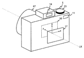
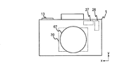
以下、本発明の第1の実施形態について、図1〜14を用いて説明する。撮像装置1はデジタルカメラであるとして説明する。なお、方向を説明するために、撮像装置1において光軸LXと直交する水平方向を第1方向x、光軸LXと直交する鉛直方向を第2方向y、光軸LXと平行な水平方向を第3方向zとして説明する。なお、図5は、図4のA−A線の断面における構成図を、図6は、図4のB−B線の断面における構成図を示す。
Hereinafter, a first embodiment of the present invention will be described with reference to FIGS. The
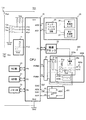
撮像装置1の撮像に関する部分は、主電源のオンオフ切り替えを行うPonボタン11、レリーズボタン13、LCDモニタ17、CPU21、撮像ブロック22、AE部23、AF部24、像ブレ補正部30の撮像部39a、及び撮影レンズ67から構成される。Ponボタン11の押下に対応してPonスイッチ11aのオンオフ状態が切り替えられ、これにより撮像装置1の主電源のオンオフ状態が切り替えられる。被写体像は、撮像部39aを駆動する撮像ブロック22によって撮影レンズ67を介した光学像として撮像され、LCDモニタ17によって撮像された画像が表示される。また被写体像は光学ファインダ(不図示)によって光学的に観察することも可能である。
The parts related to the imaging of the
レリーズボタン13は、半押しすることにより測光スイッチ12aがオン状態にされ測光や測距及び合焦動作が行われ、全押しすることによりレリーズスイッチ13aがオン状態にされ撮像が行われ、撮影像がメモリされる。
When the
CPU21は、撮像に関する各部の制御、後述する像ブレ補正に関する各部の制御を行う制御手段である。
The
撮像ブロック22は、撮像部39aを駆動する。AE部23は、被写体の測光動作を実行して露光値を演算し、この露光値に基づき撮影に必要となる絞り値及び露光時間を演算する。AF部24は、測距を行い、この測距結果に基づき撮影レンズ67を光軸方向に変位させ焦点調節を行う。
The
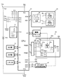
撮像装置1の像ブレ補正装置すなわち像ブレ補正に関する部分は、像ブレ補正ボタン14、CPU21、角速度検出部25、ドライバ回路29、像ブレ補正部30、ホール素子信号処理回路部45、撮影レンズ67、調整用端子71、及びメモリ部72から構成される。
The image blur correction device, that is, the image blur correction portion of the
像ブレ補正ボタン14は、押下することにより像ブレ補正スイッチ14aがオン状態にされ、測光など他の動作と独立して、一定時間ごとに、角速度検出部25、及び像ブレ補正部30が駆動されて像ブレ補正が行われる。像ブレ補正スイッチ14aがオン状態にされた補正モードの場合にパラメータIS=1、像ブレ補正スイッチ14aがオフ状態にされた補正モードでない場合にパラメータIS=0と設定する。第1の実施形態ではこの一定時間を1msであるとして説明する。
When the image
これらのスイッチの入力信号に対応する各種の出力はCPU21によって制御される。測光スイッチ12a、レリーズスイッチ13a、像ブレ補正スイッチ14aのオン/オフ情報は、それぞれ1ビットのデジタル信号としてCPU21のポートP12、P13、P14に入力される。撮像ブロック22、AE部23、及びAF部24は、それぞれポートP3、P4、P5で信号の入出力が行われる。
Various outputs corresponding to the input signals of these switches are controlled by the
調整用端子71は、後述するホール素子部44bを使用した位置検出において、位置検出に関するアナログ信号の第1、第2検出位置信号px、pyをA/D変換する際の検出分解能を上げるための初期調整を行う調整モードに入るか否かのスイッチで、オン状態にすると調整モードに入り、オフ状態にすると調整モードが解除され通常の使用モードに入る。メモリ部72は、調整モードにおいて求められた最適水平方向ホール素子電流値xDi、最適鉛直方向ホール素子電流値yDiを記録する電気的に書き換えでき、電源がオフ状態にされても内容が消去されないEEPROMなどの不揮発性メモリである。調整用端子71は、CPU21のポートP15、メモリ部72は、ポートP6で信号の入出力が行われる。
The
次に、角速度検出部25、ドライバ回路29、像ブレ補正部30、ホール素子信号処理回路部45についての詳細、及びCPU21との入出力関係について説明する。
Next, the details of the angular
角速度検出部25は、第1、第2角速度センサ26、27とアンプ・ハイパスフィルタ回路28とを有する。第1、第2角速度センサ26、27は、撮像装置1の一定時間(1ms)ごとの第1方向x及び第2方向yの角速度を検出する。第1角速度センサ26は、第1方向xの角速度を、第2角速度センサ27は第2方向yの角速度を検出する。アンプ・ハイパスフィルタ回路28は、角速度に関する信号を増幅した後、第1、第2角速度センサ26、27のヌル電圧やパンニングをカットし、第1、第2角速度vx、vyとしてアナログ信号をCPU21のA/D0、A/D1に入力する。
The angular
CPU21は、A/D0、A/D1に入力された第1、第2角速度vx、vyをA/D変換した後、焦点距離などを考慮した変換係数によって一定時間(1ms)に生じた像ブレ量を演算する。従って、角速度検出部25とCPU21は、像ブレ量演算機能を有する。
The
CPU21は、演算により求められた像ブレ量に応じた撮像部39aの移動すべき位置Sを第1方向x、第2方向yごとに演算し設定する。位置Sの第1方向x成分をsx、第2方向y成分をsyとする。撮像部39aを含む可動部30aの移動は、後述する電磁力によって行われる。可動部30aをこの位置Sまで移動させるためにドライバ回路29を駆動する駆動力Dの第1方向x成分を第1PWMデューティdx、第2方向y成分を第2PWMデューティdyとする。
The
像ブレ補正部30は、CPU21が演算した移動すべき位置Sに撮像部39aを移動させることによって、ブレによって生じた被写体像の結像面における光軸LXのずれを無くし、被写体像と結像面位置を一定に保ち、像ブレを補正する装置であり、撮像部39aを含み移動可能領域をもつ可動部30aと、固定部30bとを有する。また、像ブレ補正部30は、コイルに流れる電流の方向と磁石の磁界の向きにより生じた電磁力により可動部30aを移動させる駆動用部分と、可動部30aの位置を検出する位置検出部分とに分けて考えることもできる。
The image
像ブレ補正部30の可動部30aの駆動は、CPU21のPWM0から第1PWMデューティdx、PWM1から第2PWMデューティdyの出力を受けたドライバ回路29により行われる。ドライバ回路29の駆動により移動した可動部30aの移動前または移動後の位置Pはホール素子部44b、ホール素子信号処理回路部45によって検出される。検出された位置Pの情報は、第1検出位置信号pxが第1方向x成分として、第2検出位置信号pyが第2方向y成分としてそれぞれCPU21のA/D2、A/D3に入力される。第1、第2検出位置信号px、pyはA/D2、A/D3を介してA/D変換される。第1、第2検出位置信号px、pyに対してA/D変換後の位置Pの第1方向x成分、第2方向y成分をそれぞれpdx、pdyとする。検出された位置P(pdx、pdy)のデータと移動すべき位置S(sx、sy)のデータによりPID制御が行われる。
Driving of the
可動部30aは、第1、第2駆動用コイル31a、32a、撮像部39a、位置検出用磁石41a、可動基板49a、移動用シャフト50a、第1〜第3水平移動用軸受け部51a〜53a、プレート64aとを有する。
The
固定部30bは、第1、第2駆動用磁石33b、34b、第1、第2駆動用ヨーク35b、36b、位置検出用ヨーク43b、ホール素子部44b、第1〜第4鉛直移動用軸受け部54b〜57b、ベース板65bとを有する。
The fixed
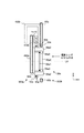
可動部30aの第3方向zから見てコの字型をした移動用シャフト50aは、固定部30bのベース板65bに取り付けられた第1〜第4鉛直移動用軸受け部54b〜57bと鉛直方向(第2方向y)に移動自在に支持される。第1、第2鉛直移動用軸受け部54b、55bは、第1方向xからみて第2方向yに延びる長穴形状を有している。これにより、可動部30aは、固定部30bに対して鉛直方向に移動が可能になる。
The U-shaped moving
また移動用シャフト50aは、可動部30aの第1〜第3水平移動用軸受け部51a〜53aと水平方向(第1方向x)に移動自在に支持される。これにより、移動用シャフト50aを除く可動部30aは、移動用シャフト50a及び固定部30bに対して水平方向に移動が可能になる。
The moving
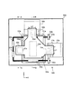
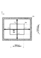
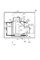
可動部30aの移動範囲について、第1方向xの一方の端点をrx11、他方の端点をrx12とし、第2方向yの一方の端点をry11、他方の端点をry12とする(図7参照)。ここでいう可動部30aの移動範囲とは、可動部30aの中心点が移動しうる範囲をいう。なお、図7は、可動部30a、固定部30bの形状を簡略化している。
Regarding the movement range of the
撮像素子39a1の撮像範囲を最大限活用するために、撮影レンズ67の光軸LXが撮像素子39a1の中心近傍を通る位置関係にある時に、第1方向x、第2方向yともに可動部30aが移動範囲の中心に位置する(移動中心位置にある)ように可動部30aと固定部30bの位置関係を設定する。撮像素子39a1の中心とは、撮像素子39a1の撮像面を形成する矩形が有する2つの対角線の交点をいう。
In order to make maximum use of the imaging range of the image sensor 39a1, when the optical axis LX of the
可動部30aは、撮影レンズ67の方向からみて光軸方向に撮像部39a、プレート64a、可動基板49aが取り付けられる。撮像部39aは、撮像素子39a1、ステージ39a2、押さえ部39a3、光学ローパスフィルタ39a4とを有し、ステージ39a2とプレート64aとで撮像素子39a1、押さえ部39a3、光学ローパスフィルタ39a4を挟み付勢する。第1〜第3水平移動用軸受け部51a〜53aは、ステージ39a2に取り付けられる。プレート64aは、撮像素子39a1が取り付けられることにより、撮像素子39a1が撮影レンズ67の光軸LXに垂直になるように位置決めを行う。またプレート64aが金属材料で出来ている場合には、撮像素子39a1と接触することによりさらに放熱効果も有する。
The
可動基板49aは、シート状でかつ渦巻き状のコイルパターンが形成された第1、第2駆動用コイル31a、32a、及び位置検出用磁石41aとが取り付けられている。第1駆動用コイル31aは、第1駆動用コイル31aの電流の方向と第1駆動用磁石33bの磁界の向きから生じる電磁力により第1駆動用コイル31aを含む可動部30aを第1方向xに移動させるべく、第1方向x、第2方向yのいずれか一方と平行な線で形成されるコイルパターンを有する。第2駆動用コイル32aは、第2駆動用コイル32aの電流の方向と第2駆動用磁石34bの磁界の向きから生じる電磁力により第2駆動用コイル32aを含む可動部30aを第2方向yに移動させるべく、第1方向x、第2方向yのいずれか一方と平行な線で形成されるコイルパターンを有する。
The
本実施形態では、第3方向zで且つ撮影レンズ67と逆方向から見て、第1駆動用コイル31aは可動基板49aの右端部(第1方向xの一方の端部)に、第2駆動用コイル32aは可動基板49aの上端部(第2方向yの一方の端部)に、位置検出用磁石41aは可動基板49aの左端部(第1方向xの他方の端部)に取り付けられる。撮像素子39a1は、可動基板49a上の第1駆動用コイル31aと位置検出用磁石41aとの間に取り付けられる。第1、第2駆動用コイル31a、32a、撮像素子39a1、及び位置検出用磁石41aは、可動基板49aの同じ側に取り付けられる。
In the present embodiment, when viewed in the third direction z and in the direction opposite to the photographing
第1、第2駆動用コイル31a、32aは、フレキシブル基板(不図示)を介してこれらを駆動するドライバ回路29と接続される。ドライバ回路29は、CPU21のPWM0、PWM1から第1、第2PWMデューティdx、dyのそれぞれが入力される。ドライバ回路29は、入力された第1、第2PWMデューティdx、dyの値に応じて第1、第2駆動用コイル31a、32aに電力を供給し、可動部30aを駆動する。
The first and second driving coils 31a and 32a are connected to a
位置検出用磁石41aは、第3方向zにN極とS極が並べて取り付けられる。また、位置検出用磁石41aの固定部30bと対向する面は、第1方向x、第2方向yのいずれか一方に平行な線で形成される正方形である。位置検出用磁石41aの固定部30bと対向する面の形状を正方形にしたことにより、可動部30aを第2方向yに移動させた時、第1方向xの位置検出に影響が及ばず、第1方向xに移動させた時、第2方向yの位置検出に影響が及ばない。
The
また、1つの磁石で、第1、第2水平方向ホール素子hh1、hh2を使った第1方向の位置検出、及び第1、第2鉛直方向ホール素子hv1、hv2を使った第2方向yの位置検出を行うことが可能になる。 Also, with one magnet, position detection in the first direction using the first and second horizontal hall elements hh1 and hh2, and the second direction y using the first and second vertical hall elements hv1 and hv2 are performed. Position detection can be performed.
第1、第2駆動用磁石33b、34bは、それぞれ第1、第2駆動用コイル31a、32aと対向するように固定部30bの可動部30a側に取り付けられる。ホール素子部44bは、位置検出用磁石41aと対向するように固定部30bの可動部30a側に取り付けられる。位置検出用ヨーク43bは固定部30bのホール素子部44bがある面と反対側、すなわち位置検出用磁石41aと対向するホール素子部44bの背面側に取り付けられる。位置検出用ヨーク43bは、磁性体材料で構成され、位置検出用磁石41aとホール素子部44bの間の磁束密度を高める役目を果たす。
The first and
第1駆動用磁石33bは、第3方向zにおいて固定部30bのベース板65b上で且つ可動部30a側に取り付けられた第1駆動用ヨーク35bの上であって、第1方向xにN極とS極が並べて取り付けられる。第1駆動用磁石33bの第2方向yの長さは、可動部30aが第2方向yに移動した際に第1駆動用コイル31aに及ぼす磁界が変化しない程度に第1駆動用コイル31aの第2方向yの第1有効長L1に比べて長めに設定される。
The
第2駆動用磁石34bは、第3方向zにおいて固定部30bのベース板65b上で且つ可動部30a側に取り付けられた第2駆動用ヨーク36bの上であって、第2方向yにN極とS極が並べて取り付けられる。第2駆動用磁石34bの第1方向xの長さは、可動部30aが第1方向xに移動した際に第2駆動用コイル32aに及ぼす磁界が変化しない程度に第2駆動用コイル32aの第1方向xの第2有効長L2に比べて長めに設定される。
The
第1駆動用ヨーク35bは、第2方向yから見てコの字型形状を有する多角柱の軟磁性体材料で構成され、第1駆動用磁石33b、及び第1駆動用コイル31aを第3方向zで挟む形で、固定部30bのベース板65b上に取り付けられる。第1駆動用ヨーク35bにおける第1駆動用磁石33bと接する側の部分は、第1駆動用磁石33bの磁界が周囲に漏れないようにする役目を果たす。第1駆動用ヨーク35bにおける第1駆動用磁石33b、第1駆動用コイル31a、及び可動基板49aと対向する側の部分は、第1駆動用磁石33bと第1駆動用コイル31aの間の磁束密度を高める役目を果たす。
The
第2駆動用ヨーク36bは、第1方向xから見てコの字型形状を有する多角柱の軟磁性体材料で構成され、第2駆動用磁石34b、及び第2駆動用コイル32aを第3方向zで挟む形で、固定部30bのベース板65b上に取り付けられる。第2駆動用ヨーク36bにおける第2駆動用磁石34bと接する側の部分は、第2駆動用磁石34bの磁界が周囲に漏れないようにする役目を果たす。第2駆動用ヨーク36bにおける第2駆動用磁石34b、第2駆動用コイル32a、及び可動基板49aと対向する側の部分は、第2駆動用磁石34bと第2駆動用コイル32aの間の磁束密度を高める役目を果たす。
The
ホール素子部44bは、ホール効果を利用した磁電変換素子(磁界変化検出素子)であるホール素子を4つ有し、可動部30aの第1方向x、第2方向yの現在位置Pを特定するための第1検出位置信号px、第2検出位置信号pyを検出するする2軸ホール素子である。4つのホール素子のうち第1方向xの位置検出用のホール素子を第1、第2水平方向ホール素子hh1、hh2、第2方向yの位置検出用のホール素子を第1、第2鉛直方向ホール素子hv1、hv2とする。
The
第1、第2水平方向ホール素子hh1、hh2は、可動部30aの第1方向xの位置を検出するため、それぞれの入力端子は直列に配線される。第1、第2水平方向ホール素子hh1、hh2は、第3方向zから見て固定部30bのベース板65b上であって、可動部30aの位置検出用磁石41aと対向する位置に取り付けられる。
Since the first and second horizontal hall elements hh1 and hh2 detect the position of the
位置検出用磁石41aの正方形の大きさを最大限活用して位置検出を行うことを可能にするため、第1、第2水平方向ホール素子hh1、hh2の第2方向yの位置は、光軸LXが撮像素子39a1の中心近傍を通る位置関係にある時に、いずれも位置検出用磁石41aのホール素子部44bと対向する面の正方形の第2方向yの中間近傍に対向する場所にあるのが望ましい(図19参照)。第1、第2水平方向ホール素子hh1、hh2の第1方向xの位置は、光軸LXが撮像素子39a1の中心近傍を通る位置関係にある時に、それぞれ位置検出用磁石41aのホール素子部44bと対向する面の正方形の第1方向xの両端部近傍に対向する場所にあるのが望ましい。
In order to make it possible to perform position detection by making maximum use of the square size of the
第1、第2鉛直方向ホール素子hv1、hv2は、可動部30aの第2方向yの変位を検出するため、それぞれの入力端子は直列に配線される。第1、第2鉛直方向ホール素子hv1、hv2は、第3方向zから見て固定部30bのベース板65b上であって、可動部30aの位置検出用磁石41aと対向する位置に取り付けられる。
Since the first and second vertical hall elements hv1 and hv2 detect the displacement of the
位置検出用磁石41aの正方形の大きさを最大限活用して位置検出を行うことを可能にするため、第1、第2鉛直方向ホール素子hv1、hv2の第1方向xの位置は、光軸LXが撮像素子39a1の中心近傍を通る位置関係にある時に、いずれも位置検出用磁石41aのホール素子部44bと対向する面の正方形の第1方向xの中間近傍に対向する場所にあるのが望ましい。第1、第2鉛直方向ホール素子hv1、hv2の第2方向yの位置は、光軸LXが撮像素子39a1の中心近傍を通る位置関係にある時に、それぞれ位置検出用磁石41aのホール素子部44bと対向する面の正方形の第2方向yの両端部近傍に対向する場所にあるのが望ましい。
In order to make it possible to perform position detection by making maximum use of the square size of the
ベース板65bは、固定部30bにおいてホール素子部44bなどを取り付けるベースとなる板状部材で、撮像素子39a1の撮像面と平行に配置される。第1の実施形態では、ベース板65bは、第3方向zにおいて、可動基板49aよりも撮影レンズ67に近い側にあるが、可動基板49aの方が撮影レンズ67に近い側にあるような位置関係であってもよい。この場合、第1、第2駆動用コイル31a、32a、位置検出用磁石41aは可動基板49aの撮影レンズ67がある側と逆側に、第1、第2駆動用磁石33b、34b、ホール素子部44bはベース板65bの撮影レンズ67がある側に配置される。
The
ホール素子信号処理回路部45は、第1、第2水平方向ホール素子hh1、hh2の出力信号から第1、第2水平方向ホール素子hh1、hh2それぞれにおける出力端子間の第1、第2水平方向電位差x1、x2を検出し、これらから第1方向xの位置を特定する第1検出位置信号pxをCPU21のA/D2に出力する。また、ホール素子信号処理回路部45は、第1、第2鉛直方向ホール素子hv1、hv2の出力信号から第1、第2鉛直方向ホール素子hv1、hv2それぞれにおける出力端子間の第1、第2鉛直方向電位差y1、y2を検出し、これらから第2方向yの位置を特定する第2検出位置信号pyをCPU21のA/D3に出力する。
The Hall element signal
位置検出時に、第1、第2水平方向ホール素子hh1、hh2それぞれの入力端子に流す電流値(最適水平方向ホール素子電流値xDi)は第1初期調整によって、第1、第2鉛直方向ホール素子hv1、hv2それぞれの入力端子に流す電流値(最適鉛直方向ホール素子電流値yDi)は、第2初期調整によって求められる。 At the time of position detection, the current value (optimum horizontal hall element current value xDi) that flows through the input terminals of the first and second horizontal hall elements hh1 and hh2 is adjusted by the first initial adjustment to the first and second vertical hall elements. The current value (optimum vertical hall element current value yDi) flowing through the input terminals of hv1 and hv2 is obtained by the second initial adjustment.
第1、第2初期調整は、ホール素子信号処理回路部45から出力される第1、第2検出位置信号px、pyを、それぞれCPU21のA/D2、A/D3を介してA/D変換される際に第1の検出分解能、第2の検出分解能を上げる、すなわち可動部30aの移動範囲内で且つCPU21がA/D変換できる範囲内で第1、第2検出位置信号px、pyそれぞれの出力値の幅を最大にする。
In the first and second initial adjustments, the first and second detection position signals px and py output from the Hall element signal
具体的に、第1初期調整は、可動部30aが第1方向xの一方の端点rx11にあって、第1検出位置信号pxの出力値がCPU21でA/D変換が可能な範囲内で最大(MAX)値となる時の第1水平方向ホール素子hh1の入力端子に流れる第1水平方向ホール素子電流値xDi1、及び可動部30aが第1方向xの他方の端点rx12にあって、第1検出位置信号pxの出力値がCPU21でA/D変換が可能な範囲内で最小(MIN)値となる時の第1水平方向ホール素子hh1の入力端子に流れる第2水平方向ホール素子電流値xDi2を求め、第1、第2水平方向ホール素子電流値xDi1、xDi2のうち小さい方の値を最適水平方向ホール素子電流値xDiとして、メモリ部72に記録する。なお、第1、第2水平方向ホール素子hh1、hh2の入力端子は直列に接続されているので、第1、第2水平方向ホール素子電流値xDi1、xDi2を求めるにあたっては、第2水平方向ホール素子hh2の入力端子の電流値を測定して求めても良い。
Specifically, the first initial adjustment is performed as long as the
具体的に、第2初期調整は、可動部30aが第2方向yの一方の端点ry11にあって、第2検出位置信号pyの出力値がCPU21でA/D変換が可能な範囲内で最大(MAX)値となる時の第1鉛直方向ホール素子hv1の入力端子に流れる第1鉛直方向ホール素子電流値yDi1、及び可動部30aが第2方向yの他方の端点ry12にあって、第2検出位置信号pyの出力値がCPU21でA/D変換が可能な範囲内で最小(MIN)値となる時の第1鉛直方向ホール素子hv1の入力端子に流れる第2鉛直方向ホール素子電流値yDi2を求め、第1、第2鉛直方向ホール素子電流値yDi1、yDi2のうち小さい方の値を最適鉛直方向ホール素子電流値yDiとして、メモリ部72に記録する。なお、第1、第2鉛直方向ホール素子hv1、hv2の入力端子は直列に接続されているので、第1、第2鉛直方向ホール素子電流値yDi1、yDi2を求めるにあたっては、第2鉛直方向ホール素子hv2の入力端子の電流値を測定して求めても良い。
Specifically, in the second initial adjustment, the
ホール素子信号処理回路部45の第6回路456は、CPU21のD/A0から最適水平方向ホール素子電流値xDiに対応した第1定電圧XVfの印加を受け、ホール素子信号処理回路部45の第16回路466は、CPU21のD/A1から最適鉛直方向ホール素子電流値yDiに対応した第2定電圧YVfの印加を受ける。
The
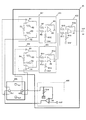
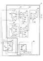
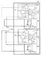
ホール素子信号処理回路部45における第1、第2水平方向ホール素子hh1、hh2の入出力信号に関する回路構成は図8で説明する。ホール素子信号処理回路部45における第1、第2鉛直方向ホール素子hv1、hv2の入出力信号に関する回路構成は図9で説明する。説明の簡略化のため、図8では、第1、第2鉛直方向ホール素子hv1、hv2に関する回路構成を省略し、図9では、第1、第2水平方向ホール素子hh1、hh2に関する回路構成を省略している。
A circuit configuration relating to input / output signals of the first and second horizontal hall elements hh1 and hh2 in the hall element signal
ホール素子信号処理回路部45における第1、第2水平方向ホール素子hh1、hh2の出力部は第1〜第5回路451〜455を有し、入力部は第6回路456を有する。ホール素子信号処理回路部45における第1、第2鉛直方向ホール素子hv1、hv2の出力部は第11〜第15回路461〜465を有し、入力部は第16回路466を有する。
The output parts of the first and second horizontal
第1水平方向ホール素子hh1の出力端子のそれぞれは、第1回路451と接続され、第1回路451は、第3回路453と接続される。第2水平方向ホール素子hh2の出力端子のそれぞれは、第2回路452と接続され、第2回路452は、第4回路454と接続される。第3、第4回路453、454は、第5回路455と接続される。第1、第2回路451、452は、それぞれ第1、第2水平方向ホール素子hh1、hh2の出力端子間における信号差を増幅する差動増幅回路である。第3回路453は増幅した信号差と基準電圧Vrefとの差異から第1水平方向ホール素子hh1における出力端子間の第1水平方向電位差x1を求める減算回路である。第4回路454は増幅した信号差と基準電圧Vrefとの差異から第2水平方向ホール素子hh2における出力端子間の第2水平方向電位差x2を求める減算回路である。第5回路455は第1、第2水平方向電位差x1、x2の差異に一定の第1増幅率AA1を乗算して第1検出位置信号pxを求める減算増幅回路である。
Each of the output terminals of the first horizontal hall element hh1 is connected to the
第1回路451は、第1〜第3抵抗R1〜R3、第1、第2オペアンプA1、A2とを有する。第1水平方向ホール素子hh1の出力端子の一方は、第1オペアンプA1の非反転入力端子と接続され、もう一方の端子は、第2オペアンプA2の非反転入力端子と接続される。第1オペアンプA1の反転入力端子は第1、第2抵抗R1、R2と接続され、第2オペアンプA2の反転入力端子は第1、第3抵抗R1、R3と接続される。第1オペアンプA1の出力端子は第2抵抗R2及び第3回路453の第7抵抗R7と接続される。第2オペアンプA2の出力端子は第3抵抗R3及び第3回路453の第9抵抗R9と接続される。
The
第2回路452は、第4〜第6抵抗R4〜R6、第3、第4オペアンプA3、A4とを有する。第2水平方向ホール素子hh2の出力端子の一方は、第3オペアンプA3の非反転入力端子と接続され、もう一方の端子は、第4オペアンプA4の非反転入力端子と接続される。第3オペアンプA3の反転入力端子は第4、第5抵抗R4、R5と接続され、第4オペアンプA4の反転入力端子は第4、第6抵抗R4、R6と接続される。第3オペアンプA3の出力端子は第5抵抗R5及び第4回路454の第11抵抗R11と接続される。第4オペアンプA4の出力端子は第6抵抗R6及び第4回路454の第13抵抗R13と接続される。
The
第3回路453は、第7〜第10抵抗R7〜R10、第5オペアンプA5とを有する。第5オペアンプA5の反転入力端子は第7抵抗R7及び第8抵抗R8と接続され、非反転入力端子は第9抵抗R9及び第10抵抗R10と接続され、出力端子は第8抵抗R8及び第5回路455の第15抵抗R15と接続され、第1水平方向電位差x1が出力される。第10抵抗R10の一方の端子は基準電圧Vrefの電源に接続される。
The
第4回路454は、第11〜第14抵抗R11〜R14、第6オペアンプA6とを有する。第6オペアンプA6の反転入力端子は第11抵抗R11及び第12抵抗R12と接続され、非反転入力端子は第13抵抗R13及び第14抵抗R14と接続され、出力端子は第12抵抗R12及び第5回路455の第17抵抗R17と接続され、第2水平方向電位差x2が出力される。第14抵抗R14の一方の端子は基準電圧Vrefの電源に接続される。
The
第5回路455は、第15〜第18抵抗R15〜R18、第7オペアンプA7とを有する。第7オペアンプA7の反転入力端子は第15抵抗R15及び第16抵抗R16と接続され、非反転入力端子は第17抵抗R17及び第18抵抗R18と接続され、出力端子は第16抵抗R16と接続され、第1、第2水平方向電位差x1、x2の差異に一定の第1増幅率AA1が乗算された第1検出位置信号pxが出力される。第18抵抗R18の一方の端子は基準電圧Vrefの電源に接続される。
The
第1、第4抵抗R1、R4は同じ抵抗値、第2、第3、第5、第6抵抗R2、R3、R5、R6は同じ抵抗値、第7〜14抵抗R7〜R14は同じ抵抗値、第15、第17抵抗R15、R17は同じ抵抗値、第16、第18抵抗R16、R18は同じ抵抗値に設定される。第1〜第4オペアンプA1〜A4は同じオペアンプ、第5、第6オペアンプA5、A6は同じオペアンプが設定される。第1増幅率AA1の値は、第16抵抗R16と、第15抵抗R15の抵抗値の割合から算出される。 The first and fourth resistors R1 and R4 have the same resistance value, the second, third, fifth, and sixth resistors R2, R3, R5, and R6 have the same resistance value, and the seventh to fourteenth resistors R7 to R14 have the same resistance value. The fifteenth and seventeenth resistors R15 and R17 are set to the same resistance value, and the sixteenth and eighteenth resistors R16 and R18 are set to the same resistance value. The first to fourth operational amplifiers A1 to A4 are set to the same operational amplifier, and the fifth and sixth operational amplifiers A5 and A6 are set to the same operational amplifier. The value of the first amplification factor AA1 is calculated from the ratio of the resistance values of the sixteenth resistor R16 and the fifteenth resistor R15.
第6回路456は、第19抵抗R19、第8オペアンプA8とを有する。第8オペアンプA8の反転入力端子は第19抵抗R19及び第2水平方向ホール素子hh2の入力端子の一方と接続される。第8オペアンプA8の非反転入力端子の電位は第1、第2水平方向ホール素子hh1、hh2それぞれの入力端子における定電流値(最適水平方向ホール素子電流値xDi)に対応した第1定電圧XVfに設定される。第1定電圧XVfの値は、最適水平方向ホール素子電流値xDiに第19抵抗R19の抵抗値を乗算して求められる。第1定電圧XVfは、CPU21のD/A0から印加される。第8オペアンプA8の出力端子は第1水平方向ホール素子hh1の入力端子の一方と接続される。第19抵抗R19の一方の端子は接地される。
The
第1鉛直方向ホール素子hv1の出力端子のそれぞれは、第11回路461と接続され、第11回路461は、第13回路463と接続される。第2鉛直方向ホール素子hv2の出力端子のそれぞれは、第12回路462と接続され、第12回路462は、第14回路464と接続される。第13、第14回路463、464は、第15回路465と接続される。第11、第12回路461、462は、それぞれ第1、第2鉛直方向ホール素子hv1、hv2の出力端子間における信号差を増幅する差動増幅回路である。第13回路463は増幅した信号差と基準電圧Vrefとの差異から第1鉛直方向ホール素子hv1における出力端子間の第1鉛直方向電位差y1を求める減算回路である。第14回路464は増幅した信号差と基準電圧Vrefとの差異から第2鉛直方向ホール素子hv2における出力端子間の第2鉛直方向電位差y2を求める減算回路である。第15回路465は第1、第2鉛直方向電位差y1、y2の差異に一定の第2増幅率AA2を乗算して第2検出位置信号pyを求める減算増幅回路である。
Each of the output terminals of the first vertical hall element hv1 is connected to the
第11回路461は、第21〜第23抵抗R21〜R23、第21、第22オペアンプA21、A22とを有する。第1鉛直方向ホール素子hv1の出力端子の一方は、第21オペアンプA21の非反転入力端子と接続され、もう一方の端子は、第22オペアンプA22の非反転入力端子と接続される。第21オペアンプA21の反転入力端子は第21、第22抵抗R21、R22と接続され、第22オペアンプA22の反転入力端子は第21、第23抵抗R21、R23と接続される。第21オペアンプA21の出力端子は第22抵抗R22及び第13回路463の第27抵抗R27と接続される。第22オペアンプA22の出力端子は第23抵抗R23及び第13回路463の第29抵抗R29と接続される。
The
第12回路462は、第24〜第26抵抗R24〜R26、第23、第24オペアンプA23、A24とを有する。第2鉛直方向ホール素子hv2の出力端子の一方は、第23オペアンプA23の非反転入力端子と接続され、もう一方の端子は、第24オペアンプA24の非反転入力端子と接続される。第23オペアンプA23の反転入力端子は第24、第25抵抗R24、R25と接続され、第24オペアンプA24の反転入力端子は第24、第26抵抗R24、R26と接続される。第23オペアンプA23の出力端子は第25抵抗R25及び第14回路464の第31抵抗R31と接続される。第24オペアンプA24の出力端子は第26抵抗R26及び第14回路464の第33抵抗R33と接続される。
The
第13回路463は、第27〜第30抵抗R27〜R30、第25オペアンプA25とを有する。第25オペアンプA25の反転入力端子は第27抵抗R27及び第28抵抗R28と接続され、非反転入力端子は第29抵抗R29及び第30抵抗R30と接続され、出力端子は第28抵抗R28及び第15回路465の第35抵抗R35と接続され、第1鉛直方向電位差y1が出力される。第30抵抗R30の一方の端子は基準電圧Vrefの電源に接続される。
The
第14回路464は、第31〜第34抵抗R31〜R34、第26オペアンプA26とを有する。第26オペアンプA26の反転入力端子は第31抵抗R31及び第32抵抗R32と接続され、非反転入力端子は第33抵抗R33及び第34抵抗R34と接続され、出力端子は第32抵抗R32及び第15回路465の第37抵抗R37と接続され、第2鉛直方向電位差y2が出力される。第34抵抗R34の一方の端子は基準電圧Vrefの電源に接続される。
The
第15回路465は、第35〜第38抵抗R35〜R38、第27オペアンプA27とを有する。第27オペアンプA27の反転入力端子は第35抵抗R35及び第36抵抗R36と接続され、非反転入力端子は第37抵抗R37及び第38抵抗R38と接続され、出力端子は第36抵抗R36と接続され、第1、第2鉛直方向電位差y1、y2の差異に一定の第2増幅率AA2が乗算された第2検出位置信号pyが出力される。第38抵抗R38の一方の端子は基準電圧Vrefの電源に接続される。
The
第21、第24抵抗R21、R24は同じ抵抗値、第22、第23、第25、第26抵抗R22、R23、R25、R26は同じ抵抗値、第27〜34抵抗R27〜R34は同じ抵抗値、第35、第37抵抗R35、R37は同じ抵抗値、第36、第38抵抗R36、R38は同じ抵抗値に設定される。第21〜第24オペアンプA21〜A24は同じオペアンプ、第25、第26オペアンプA25、A26は同じオペアンプが設定される。第2増幅率AA2の値は、第36抵抗R36と、第35抵抗R35の抵抗値の割合から算出される。 The twenty-first and twenty-fourth resistors R21 and R24 have the same resistance value, the twenty-second, twenty-third, twenty-fifth and twenty-sixth resistors R22, R23, R25 and R26 have the same resistance value, and the twenty-seventh to thirty-fourth resistors R27 to R34 have the same resistance value. The 35th and 37th resistors R35 and R37 are set to the same resistance value, and the 36th and 38th resistors R36 and R38 are set to the same resistance value. The 21st to 24th operational amplifiers A21 to A24 are set to the same operational amplifier, and the 25th and 26th operational amplifiers A25 and A26 are set to the same operational amplifier. The value of the second amplification factor AA2 is calculated from the ratio of the resistance values of the 36th resistor R36 and the 35th resistor R35.
第16回路466は、第39抵抗R39、第28オペアンプA28とを有する。第28オペアンプA28の反転入力端子は第39抵抗R39及び第2鉛直方向ホール素子hv2の入力端子の一方と接続される。第28オペアンプA28の非反転入力端子の電位は第1、第2鉛直方向ホール素子hv1、hv2それぞれの入力端子における定電流値(最適鉛直方向ホール素子電流値yDi)に対応した第2定電圧YVfに設定される。第2定電圧YVfは、最適鉛直方向ホール素子電流値yDiに第39抵抗R39の抵抗値を乗算して求められる。第2定電圧YVfは、CPU21のD/A1から印加される。第28オペアンプA28の出力端子は第1鉛直方向ホール素子hv1の入力端子の一方と接続される。第39抵抗R39の一方の端子は接地される。
The
従来の技術では、ホール素子信号処理回路部45の第5回路455の第16、第18抵抗R16、R18、及び第15回路465の第36、第38抵抗R36、R38の抵抗値を変化させることで、第5、第15回路455、465の増幅率(第1、第2増幅率AA1、AA2)を変化させて、検出分解能を上げる初期調整を行っていた。この初期調整の方法では、抵抗値を変化させる機械的調整を伴うため、生産性に問題があった。
In the conventional technique, the resistance values of the sixteenth and eighteenth resistors R16 and R18 of the
従来技術に対して第1の実施形態では、ホール素子信号処理回路部45の抵抗値は一定すなわち増幅率(第1、第2増幅率AA1、AA2)は一定で、第1、第2水平方向ホール素子hh1、hh2の入力端子に流れる電流値を変化させる第1初期調整、及び第1、第2鉛直方向ホール素子hv1、hv2の入力端子に流れる電流値を変化させる第2初期調整を行う。
In the first embodiment, the resistance value of the Hall element signal
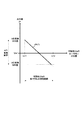
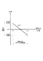
具体的に第1初期調整を、図10、図11を使って説明する。図10は、可動部30aの位置が第1方向xの一方の端点rx11にある場合の第1検出位置信号pxの出力値がCPU21のA/D変換できる最大(MAX)値と一致するよう第1、第2水平方向ホール素子hh1、hh2の入力端子に流れる電流値が調整された時の、可動部30aの第1方向xの変位と第1検出位置信号pxの出力値の関係を示す。このときの電流値を第1水平方向ホール素子電流値xDi1とする。また、図10のグラフ上の太線と破線で構成される線を第1線pfx(1)とする。第1線pfx(1)の破線部分は、可動部30aの位置が他方の端点rx12にある時の第1検出位置信号pxの出力値がCPU21のA/D変換できる最小(MIN)値を下方に超えて正確な位置検出が行えない状態を示す。
Specifically, the first initial adjustment will be described with reference to FIGS. FIG. 10 shows that the output value of the first detection position signal px when the position of the
図11は、可動部30aの位置が第1方向xの他方の端点rx12にある場合の第1検出位置信号pxの出力値がCPU21のA/D変換できる最小(MIN)値と一致するよう第1、第2水平方向ホール素子hh1、hh2の入力端子に流れる電流値が調整された時の、可動部30aの第1方向xの変位と第1検出位置信号pxの出力値の関係を示す。このときの電流値を第2水平方向ホール素子電流値xDi2とする。また、このとき、図11のグラフ上の太線を第2線pfx(2)とする。第2線pfx(2)は、可動部30aの第1方向xの位置が一方の端点rx11にある時の第1検出位置信号pxの出力値がCPU21のA/D変換できる最大(MAX)値を上方に超えておらず正確な位置検出が行える状態を示す。従って、可動部30aの第1方向xの移動範囲内では正確な位置検出が行える。
FIG. 11 shows that the output value of the first detection position signal px when the position of the
第1検出位置信号pxは、第1、第2水平方向ホール素子hh1、hh2と位置検出用磁石41aとの間の第1磁束密度B1、及び第1、第2水平方向ホール素子hh1、hh2それぞれの入力端子に流れる電流値の関数である。第2検出位置信号pyは、第1、第2鉛直方向ホール素子hv1、hv2と位置検出用磁石41aとの間の第2磁束密度B2、及び第1、第2鉛直方向ホール素子hv1、hv2の入力端子に流れる電流値の関数である。
The first detection position signal px includes the first magnetic flux density B1 between the first and second horizontal hall elements hh1 and hh2 and the
第1、第2水平方向ホール素子電流値xDi1、xDi2を比較し低い方の電流値を最適水平方向ホール素子電流値xDiとする。図10、図11の例では、第2水平方向ホール素子電流値xDi2の方が、第1水平方向ホール素子電流値xDi1よりも低くなるので、第2水平方向ホール素子電流値xDi2を最適水平方向ホール素子電流値xDiとする。第2方向yの初期調整、すなわち第2初期調整も、同様に行い最適鉛直方向ホール素子電流値yDiを求める(不図示)。最適水平方向ホール素子電流値xDi、最適鉛直方向ホール素子電流値yDiの値は、メモリ部72に記録される。
The first and second horizontal hall element current values xDi1 and xDi2 are compared, and the lower current value is set as the optimum horizontal hall element current value xDi. 10 and 11, since the second horizontal hall element current value xDi2 is lower than the first horizontal hall element current value xDi1, the second horizontal hall element current value xDi2 is set to the optimum horizontal direction. The Hall element current value is xDi. The initial adjustment in the second direction y, that is, the second initial adjustment is performed in the same manner to obtain the optimum vertical hall element current value yDi (not shown). The optimum horizontal hall element current value xDi and optimum vertical hall element current value yDi are recorded in the
可動部30aが移動中心位置にある時に、第1検出位置信号pxが基準電圧Vrefと一致する場合は、第1、第2水平方向ホール素子電流値xDi1、xDi2の値は一致する。すなわち、第1検出位置信号pxの出力値の最大をCPU21のA/D変換できる最大(MAX)値と一致するような電流値が第1、第2水平方向ホール素子hh1、hh2の入力端子に流れる時に、第1検出位置信号pxの出力値の最小はCPU21のA/D変換できる最小(MIN)値と一致する。しかし、可動部30aが移動中心位置にある時に、第1検出位置信号pxが基準電圧Vrefと厳密に一致させるには、像ブレ補正部30の機構のズレやホール素子信号処理回路部45の抵抗値の誤差を考慮した調整を別途行わなければならない。第2検出位置信号pyと、第1、第2鉛直方向ホール素子電流値yDi1、yDi2の関係も同様である。
If the first detection position signal px matches the reference voltage Vref when the
第1の実施形態では、このような調整を行って可動部30aが移動中心位置にある時に、第1検出位置信号pxが基準電圧Vrefと一致させる必要はなく、最適水平方向ホール素子電流値xDiを算出することが可能であり、第2検出位置信号pyと基準電圧Vrefと一致させる必要はなく、最適鉛直方向ホール素子電流値yDiを算出することが可能である。
In the first embodiment, when such adjustment is performed and the
また、機械的調整を伴わず第1、第2水平方向ホール素子hh1、hh2の入力端子、及び第1、第2鉛直方向ホール素子hv1、hv2の入力端子に流れる電流値を変化させる電気的調整で第1、第2初期調整を完結できるので、生産性の向上を図ることが可能になる。また、第1、第2初期調整によって求められ、メモリ部72に記録された最適水平方向ホール素子電流値xDi、最適鉛直方向ホール素子電流値yDiは電源をオフ状態にしても消去されないため、一度初期調整するだけで最適水平方向ホール素子電流値xDi、最適鉛直方向ホール素子電流値yDiを何度も使用することが可能になる。
Further, electrical adjustment is performed to change the value of current flowing through the input terminals of the first and second horizontal hall elements hh1 and hh2 and the input terminals of the first and second vertical hall elements hv1 and hv2 without mechanical adjustment. Thus, since the first and second initial adjustments can be completed, productivity can be improved. The optimum horizontal hall element current value xDi and optimum vertical hall element current value yDi obtained by the first and second initial adjustments and recorded in the
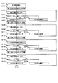
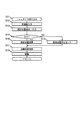
次に、第1、第2初期調整の手順を図12、図13のフローチャートで説明する。ステップS101で、調整用端子71がオン状態にされることにより撮像装置1が調整モードに入り第1、第2初期調整が開始されると、ステップS102で、CPU21のPWM0より第1PWMデューティdxがドライバ回路29に出力され、可動部30aを第1方向xの一方の端点rx11に移動させる。ステップS103で、このときの第1検出位置信号pxを検出し、CPU21のA/D2に入力する。ステップS104で、CPU21に入力された第1検出位置信号pxの出力値がCPU21のA/D変換できるMAX値と一致するか否かを判断する。一致していない場合はステップS105で、ホール素子信号処理回路部45に出力するCPU21のD/A0の出力値を変更して、ステップS103に戻る。一致している場合はステップS106で、このときの第1、第2水平方向ホール素子hh1、hh2の入力端子に流れる電流値(第1水平方向ホール素子電流値xDi1)をCPU21などで一時記録(ストア)する。
Next, the first and second initial adjustment procedures will be described with reference to the flowcharts of FIGS. In step S101, when the
ステップS107で、CPU21のPWM0より第1PWMデューティdxがドライバ回路29に出力され、可動部30aを第1方向xの他方の端点rx12に移動させる。ステップS108で、このときの第1検出位置信号pxを検出し、CPU21のA/D2に入力する。ステップS109で、CPU21に入力された第1検出位置信号pxの出力値がCPU21のA/D変換できるMIN値と一致するか否かを判断する。一致していない場合はステップS110で、ホール素子信号処理回路部45に出力するCPU21のD/A0の出力値を変更して、ステップS108に戻る。一致している場合はステップS111で、このときの第1、第2水平方向ホール素子hh1、hh2の入力端子に流れる電流値(第2水平方向ホール素子電流値xDi2)をCPU21などで一時記録(ストア)する。
In step S107, the first PWM duty dx is output from the
ステップS112で、CPU21のPWM1より第2PWMデューティdyがドライバ回路29に出力され、可動部30aを第2方向yの一方の端点ry11に移動させる。ステップS113で、このときの第2検出位置信号pyを検出し、CPU21のA/D3に入力する。ステップS114で、CPU21に入力された第2検出位置信号pyの出力値がCPU21のA/D変換できるMAX値と一致するか否かを判断する。一致していない場合はステップS115で、ホール素子信号処理回路部45に出力するCPU21のD/A1の出力値を変更して、ステップS113に戻る。一致している場合はステップS116で、このときの第1、第2鉛直方向ホール素子hv1、hv2の入力端子に流れる電流値(第1鉛直方向ホール素子電流値yDi1)をCPU21などで一時記録(ストア)する。
In step S112, the second PWM duty dy is output from the PWM1 of the
ステップS117で、CPU21のPWM1より第2PWMデューティdyがドライバ回路29に出力され、可動部30aを第2方向yの他方の端点ry12に移動させる。ステップS118で、このときの第2検出位置信号pyを検出し、CPU21のA/D3に入力する。ステップS119で、CPU21に入力された第2検出位置信号pyの出力値がCPU21のA/D変換できるMIN値と一致するか否かを判断する。一致していない場合はステップS120で、ホール素子信号処理回路部45に出力するCPU21のD/A1の出力値を変更して、ステップS118に戻る。一致している場合はステップS121で、このときの第1、第2鉛直方向ホール素子hv1、hv2の入力端子に流れる電流値(第2鉛直方向ホール素子電流値yDi2)をCPU21などで一時記録(ストア)する。
In step S117, the second PWM duty dy is output from the PWM1 of the
ステップS122で、第1水平方向ホール素子電流値xDi1が、第2水平方向ホール素子電流値xDi2よりも大きいか否かを判断する。大きくない場合は、ステップS123で、第1水平方向ホール素子電流値xDi1を最適水平方向ホール素子電流値xDiとし、ステップS125でこれをメモリ部72に記録して、第1初期調整を終了する。大きい場合は、ステップS124で、第2水平方向ホール素子電流値xDi2を最適水平方向ホール素子電流値xDiとし、ステップS125でこれをメモリ部72に記録して、第1初期調整を終了する。
In step S122, it is determined whether or not the first horizontal hall element current value xDi1 is larger than the second horizontal hall element current value xDi2. If not, in step S123, the first horizontal hall element current value xDi1 is set as the optimum horizontal hall element current value xDi, which is recorded in the
ステップS126で、第1鉛直方向ホール素子電流値yDi1が、第2鉛直方向ホール素子電流値yDi2よりも大きいか否かを判断する。大きくない場合は、ステップS127で、第1鉛直方向ホール素子電流値yDi1を最適鉛直方向ホール素子電流値yDiとし、ステップS129でこれをメモリ部72に記録して、ステップS130で第2初期調整を終了する。大きい場合は、ステップS128で、第2鉛直方向ホール素子電流値yDi2を最適鉛直方向ホール素子電流値yDiとし、ステップS129でこれをメモリ部72に記録して、ステップS130で第2初期調整を終了する。
In step S126, it is determined whether or not the first vertical hall element current value yDi1 is larger than the second vertical hall element current value yDi2. If not, in step S127, the first vertical hall element current value yDi1 is set as the optimum vertical hall element current value yDi, and is recorded in the
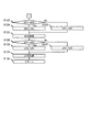
次に、一定時間(1ms)ごとに割り込み処理として他の動作と独立して行われる像ブレ補正処理について手順を図14のフローチャートで説明する。 Next, the procedure of image blur correction processing that is performed independently of other operations as interrupt processing at regular time intervals (1 ms) will be described with reference to the flowchart of FIG.
ステップS11で、像ブレ補正処理の割り込み動作が始まると、ステップS12で、角速度検出部25から出力された第1、第2角速度vx、vyが、CPU21のA/D0、A/D1を介しA/D変換され入力される。ステップS13で、ホール素子部44bで位置検出され、ホール素子信号処理回路部45で演算された第1、第2検出位置信号px、pyがCPU21のA/D2、A/D3を介しA/D変換され入力され、現在位置P(pdx、pdy)が求められる。このときのホール素子部44bの第1、第2水平方向ホール素子hh1、hh2の入力端子に流れる電流値が最適水平方向ホール素子電流値xDiになるように、CPU21はD/A0からホール素子信号処理回路部45の第6回路456に第1定電圧XVfを印加する。また、ホール素子部44bの第1、第2鉛直方向ホール素子hv1、hv2の入力端子に流れる電流値が最適鉛直方向ホール素子電流値yDiになるように、CPU21はD/A1からホール素子信号処理回路部45の第16回路466に第2定電圧YVfを印加する。
When the image blur correction process interrupt operation starts in step S11, the first and second angular velocities vx and vy output from the angular
ステップS14で、IS=0か否かが判断される。IS=0すなわち補正モードでない場合は、ステップS15で、可動部30aの移動すべき位置S(sx、sy)が、可動部30aの移動中心位置と同じに設定される。IS=1すなわち補正モードの場合は、ステップS16で、ステップS12で求めた第1、第2角速度vx、vyから可動部30aの移動すべき位置S(sx、sy)が演算され設定される。
In step S14, it is determined whether IS = 0. When IS = 0, that is, when the correction mode is not set, in step S15, the position S (sx, sy) to which the
ステップS17で、ステップS15またはステップS16で設定した位置S(sx、sy)と現在位置P(pdx、pdy)より可動部30aの移動に必要な駆動力Dすなわち第1、第2駆動用コイル31a、32aを駆動するのに必要な第1、第2PWMデューティdx、dyが演算される。ステップS18で第1、第2PWMデューティdx、dyによりドライバ回路29を介し第1、第2駆動用コイル31a、32aが駆動され可動部30aが移動せしめられる。ステップS17、S18の動作は、一般的な比例、積分、微分演算を行うPID自動制御で用いられる自動制御演算である。
In step S17, the driving force D required to move the
次に第2の実施形態としてホール素子を第1方向xの位置検出用、第2方向yの位置検出用に1つずつ計2つ使用する1軸ホール素子による位置検出を説明する。図1、図2、図7、図10〜14に関する構成は第1の実施形態と同じである。第1の実施形態における可動部30aに相当する可動部300a、第1の実施形態における固定部30bに相当する固定部300b、及び第1の実施形態におけるホール素子信号処理回路部45に相当するホール素子信号処理回路部450の構成が異なる。以下、第1の実施形態と異なる点を中心に図15〜図18を用いて説明する。第1の実施形態と同じ部位については同じ符号で表している。なお、図17は、図16のC−C線の断面における構成図を示す。
Next, as a second embodiment, position detection using a single-axis Hall element that uses a total of two Hall elements, one for position detection in the first direction x and one for position detection in the second direction y, will be described. The configuration related to FIGS. 1, 2, 7, and 10 to 14 is the same as that of the first embodiment. A
可動部300aは、第1、第2駆動用コイル31a、32a、撮像部39a、ホール素子部440a、可動基板490a、移動用シャフト50a、第1〜第3水平移動用軸受け部51a〜53a、プレート64aとを有する。
The
固定部300bは、位置検出用磁石として2つの第1、第2位置検出及び駆動用磁石411b、412b、第1、第2位置検出及び駆動用ヨーク431b、432b、第1〜第4鉛直移動用軸受け部54b〜57b、ベース板65bとを有する。
The fixed
移動用シャフト50aの構成、第1〜第4鉛直移動用軸受け部54b〜57bとの支持、及び第1〜第3水平移動用軸受け部51a〜53aとの支持については第1の実施形態と同じである。
The configuration of the moving
可動部300aの移動範囲について、第1方向xの一方の端点をrx11、他方の端点をrx12とし、第2方向yの一方の端点をry11、他方の端点をry12とする。ここでいう可動部300aの移動範囲とは、可動部300aの中心点が移動しうる範囲をいう。
Regarding the movement range of the
撮像素子39a1の撮像範囲を最大限活用するために、撮影レンズ67の光軸LXが撮像素子39a1の中心近傍を通る位置関係にある時に、第1方向x、第2方向yともに可動部300aが移動範囲の中心に位置する(移動中心位置にある)ように可動部300aと固定部300bの位置関係を設定する。撮像素子39a1の中心とは、撮像素子39a1の撮像面を形成する矩形が有する2つの対角線の交点をいう。
In order to make maximum use of the imaging range of the image sensor 39a1, when the optical axis LX of the
可動部300aは、撮影レンズ67の方向からみて光軸方向に撮像部39a、プレート64a、可動基板490aが取り付けられる。撮像部39aは、撮像素子39a1、ステージ39a2、押さえ部39a3、光学ローパスフィルタ39a4とを有し、ステージ39a2とプレート64aとで撮像素子39a1、押さえ部39a3、光学ローパスフィルタ39a4を挟み付勢する。第1〜第3水平移動用軸受け部51a〜53aは、ステージ39a2に取り付けられる。プレート64aの構成は第1の実施形態と同じである。
The
可動基板490aは、シート状でかつ渦巻き状のコイルパターンが形成された第1、第2駆動用コイル31a、32a、及びホール素子部440aとが取り付けられている。第1駆動用コイル31aは、第1駆動用コイル31aの電流の方向と第1位置検出及び駆動用磁石411bの磁界の向きから生じる電磁力により第1駆動用コイル31aを含む可動部300aを第1方向xに移動させるべく、第1方向x、第2方向yのいずれか一方と平行な線で形成されるコイルパターンを有する。第2駆動用コイル32aは、第2駆動用コイル32aの電流の方向と第2位置検出及び駆動用磁石412bの磁界の向きから生じる電磁力により第2駆動用コイル32aを含む可動部300aを第2方向yに移動させるべく、第1方向x、第2方向yのいずれか一方と平行な線で形成されるコイルパターンを有する。ホール素子部440aについては後述する。
The
第1、第2駆動用コイル31a、32aとドライバ回路29との接続については、第1の実施形態と同じである。
The connection between the first and second drive coils 31a and 32a and the
第1位置検出及び駆動用磁石411bは、第1駆動用コイル31a及び水平方向ホール素子hh10と対向するように固定部300bの可動部300a側に取り付けられる。第2位置検出及び駆動用磁石412bは、第2駆動用コイル32a及び鉛直方向ホール素子hv10と対向するように固定部300bの可動部300a側に取り付けられる。
The first position detection and drive
第1位置検出及び駆動用磁石411bは、第3方向zにおいて固定部300bのベース板65b上で且つ可動部300a側に取り付けられた第1位置検出及び駆動用ヨーク431bの上であって、第1方向xにN極とS極が並べて取り付けられる。第1位置検出及び駆動用磁石411bの第2方向yの長さは、可動部300aが第2方向yに移動した際に第1駆動用コイル31a及び水平方向ホール素子hh10に及ぼす磁界が変化しない程度に第1駆動用コイル31aの第2方向yの第1有効長L1に比べて長めに設定される。
The first position detection and drive
第2位置検出及び駆動用磁石412bは、第3方向zにおいて固定部300bのベース板65b上で且つ可動部300a側に取り付けられた第2位置検出及び駆動用ヨーク432bの上であって、第2方向yにN極とS極が並べて取り付けられる。第2位置検出及び駆動用磁石412bの第1方向xの長さは、可動部300aが第1方向xに移動した際に第2駆動用コイル32a及び鉛直方向ホール素子hv10に及ぼす磁界が変化しない程度に第2駆動用コイル32aの第1方向xの第2有効長L2に比べて長めに設定される。
The second position detection and drive
第1位置検出及び駆動用ヨーク431bは、第2方向yから見てコの字型形状を有する多角柱の軟磁性体材料で構成され、第1位置検出及び駆動用磁石411b、第1駆動用コイル31a、及び水平方向ホール素子hh10を第3方向zで挟む形で、固定部300bのベース板65b上に取り付けられる。第1位置検出及び駆動用ヨーク431bにおける第1位置検出及び駆動用磁石411bと接する側の部分は、第1位置検出及び駆動用磁石411bの磁界が周囲に漏れないようにする役目を果たす。第1位置検出及び駆動用ヨーク431bにおける第1位置検出及び駆動用磁石411b、第1駆動用コイル31a、及び可動基板490aと対向する側の部分は、第1位置検出及び駆動用磁石411bと第1駆動用コイル31a、及び第1位置検出及び駆動用磁石411bと水平方向ホール素子hh10との間の磁束密度を高める役目を果たす。
The first position detecting / driving
第2位置検出及び駆動用ヨーク432bは、第1方向xから見てコの字型形状を有する多角柱の軟磁性体材料で構成され、第2位置検出及び駆動用磁石412b、第2駆動用コイル32a、及び鉛直方向ホール素子hv10を第3方向zで挟む形で、固定部300bのベース板65b上に取り付けられる。第2位置検出及び駆動用ヨーク432bにおける第2位置検出及び駆動用磁石412bと接する側の部分は、第2位置検出及び駆動用磁石412bの磁界が周囲に漏れないようにする役目を果たす。第2位置検出及び駆動用ヨーク432bにおける第2位置検出及び駆動用磁石412b、第2駆動用コイル32a、及び可動基板490aと対向する側の部分は、第2位置検出及び駆動用磁石412bと第2駆動用コイル32a、及び第2位置検出及び駆動用磁石412bと鉛直方向ホール素子hv10との間の磁束密度を高める役目を果たす。
The second position detection and drive
ホール素子部440aは、ホール効果を利用した磁電変換素子であるホール素子を2つ有し、可動部300aの第1方向x、第2方向yの現在位置P(第1検出位置信号px、第2検出位置信号py)を検出する1軸ホール素子である。2つのホール素子のうち第1方向xの位置検出用のホール素子を水平方向ホール素子hh10、第2方向yの位置検出用のホール素子を鉛直方向ホール素子hv10とする。
The
水平方向ホール素子hh10は、第3方向zから見て可動部300aの可動基板490a上であって、固定部300bの第1位置検出及び駆動用磁石411bと対向する位置に取り付けられる。鉛直方向ホール素子hv10は、第3方向zから見て可動部300aの可動基板490a上であって、固定部300bの第2位置検出及び駆動用磁石412bと対向する位置に取り付けられる。
The horizontal hall element hh10 is mounted on the
ベース板65bは、固定部30bにおいて第1、第2位置検出及び駆動用ヨーク431b、432bなどを取り付けるベースとなる板状部材で、撮像素子39a1の撮像面と平行に配置される。第2の実施形態では、ベース板65bは、第3方向zにおいて、可動基板490aよりも撮影レンズ67に近い側にあるが、可動基板490aの方が撮影レンズ67に近い側にあるような位置関係であってもよい。この場合、第1、第2駆動用コイル31a、32a、ホール素子部440aは可動基板490aの撮影レンズ67がある側と逆側に、第1、第2位置検出及び駆動用磁石411b、412bはベース板65bの撮影レンズ67がある側に配置される。
The
ホール素子信号処理回路部450は、水平方向ホール素子hh10の出力信号から水平方向ホール素子hh10における出力端子間の水平方向電位差x10を検出し、これから第1方向xの位置を特定する第1検出位置信号pxをCPU21のA/D2に出力する第1ホール素子信号処理回路4501と、鉛直方向ホール素子hv10の出力信号から、鉛直方向ホール素子hv10における出力端子間の鉛直方向電位差y10を検出し、これから第2方向yの位置を特定する第2検出位置信号pyをCPU21のA/D3に出力する第2ホール素子信号処理回路4502とを有する。
The hall element signal
第1ホール素子信号処理回路4501は、CPU21のD/A0から最適水平方向ホール素子電流値xDiに対応した第1定電圧XVfの印加を受ける。第2ホール素子信号処理回路4502は、CPU21のD/A1から最適鉛直方向ホール素子電流値yDiに対応した第2定電圧YVfの印加を受ける。
The first hall element
第1、第2ホール素子信号処理回路4501、4502における水平方向ホール素子hh10、鉛直方向ホール素子hv10それぞれの入出力信号に関する回路構成を説明する(図18参照)。
A circuit configuration relating to input / output signals of the horizontal hall element hh10 and the vertical hall element hv10 in the first and second hall element
第1ホール素子信号処理回路4501における水平方向ホール素子hh10の出力部は第101回路4510、第103回路4530を有し、入力部は第106回路4560を有する。第2ホール素子信号処理回路4502における鉛直方向ホール素子hv10の出力部は第111回路4610、第113回路4630を有し、入力部は第116回路4660を有する。
In the first hall element
水平方向ホール素子hh10の出力端子は、第101回路4510と接続され、第101回路4510は、第103回路4530と接続される。第101回路4510は、水平方向ホール素子hh10の出力端子間における信号差を増幅する差動増幅回路である。第103回路4530は増幅した信号差と基準電圧Vrefとの差異から水平方向ホール素子hh10における出力端子間の水平方向電位差x10(ホール出力電圧)を求め、これに一定の第1増幅率AA1を乗算して第1検出位置信号pxを求める減算増幅回路である。
The output terminal of the horizontal hall element hh10 is connected to the
第101回路4510の構成は、第1の実施形態における第1回路451と同じで、第101〜第103抵抗R101〜R103、第101、第102オペアンプA101、A102とを有する。水平方向ホール素子hh10の出力端子の一方は、第101オペアンプA101の非反転入力端子と接続され、もう一方の端子は、第102オペアンプA102の非反転入力端子と接続される。第101オペアンプA101の反転入力端子は第101、第102抵抗R101、R102と接続され、第102オペアンプA102の反転入力端子は第101、第103抵抗R101、R103と接続される。第101オペアンプA101の出力端子は第102抵抗R102及び第103回路4530の第107抵抗R107と接続される。第102オペアンプA102の出力端子は第103抵抗R103及び第103回路4530の第109抵抗R109と接続される。
The configuration of the
第103回路4530の構成は、第1の実施形態における第3回路453と同じであり、第107〜第110抵抗R107〜R110、第105オペアンプA105とを有する。第105オペアンプA105の反転入力端子は第107抵抗R107及び第108抵抗R108と接続され、非反転入力端子は第109抵抗R109及び第110抵抗R110と接続され、出力端子は第108抵抗R108と接続され、水平方向電位差x10に一定の第1増幅率AA1を乗算した第1検出位置信号pxが出力される。第110抵抗R110の一方の端子は基準電圧Vrefの電源に接続される。
The configuration of the
第102、第103抵抗R102、R103は同じ抵抗値、第107、第109抵抗R107、R109は同じ抵抗値、第108、第110抵抗R108、R110は同じ抵抗値に設定される。第1増幅率AA1の値は、第108抵抗R108と、第107抵抗R107の抵抗値の割合から算出される。 The 102nd and 103rd resistors R102 and R103 are set to the same resistance value, the 107th and 109th resistors R107 and R109 are set to the same resistance value, and the 108th and 110th resistors R108 and R110 are set to the same resistance value. The value of the first amplification factor AA1 is calculated from the ratio of the resistance values of the 108th resistor R108 and the 107th resistor R107.
第106回路4560の構成は、第1の実施形態における第6回路456と同じで、第119抵抗R119、第108オペアンプA108とを有する。第108オペアンプA108の反転入力端子は第119抵抗R119及び水平方向ホール素子hh10の入力端子の一方と接続される。第108オペアンプA108の非反転入力端子の電位は水平方向ホール素子hh10の入力端子における定電流値(最適水平方向ホール素子電流値xDi)に対応した第1定電圧XVfに設定される。第1定電圧XVfの値は、最適水平方向ホール素子電流値xDiに第119抵抗R119の抵抗値を乗算して求められる。第108オペアンプA108の出力端子は水平方向ホール素子hh10の入力端子の一方と接続される。第119抵抗R119の一方の端子は接地される。
The configuration of the
鉛直方向ホール素子hv10の出力端子は、第111回路4610と接続され、第111回路4610は、第113回路4630と接続される。第111回路4610は、鉛直方向ホール素子hv10の出力端子間における信号差を増幅する差動増幅回路である。第113回路4630は増幅した信号差と基準電圧Vrefとの差異から鉛直方向ホール素子hv10における出力端子間の鉛直方向電位差y10(ホール出力電圧)を求め、これに一定の第2増幅率AA2を乗算して第2検出位置信号pyを求める減算増幅回路である。
The output terminal of the vertical hall element hv10 is connected to the
第111回路4610の構成は、第1の実施形態における第11回路461と同じで、第121〜第123抵抗R121〜R123、第121、第122オペアンプA121、A122とを有する。鉛直方向ホール素子hv10の出力端子の一方は、第121オペアンプA121の非反転入力端子と接続され、もう一方の端子は、第122オペアンプA122の非反転入力端子と接続される。第121オペアンプA121の反転入力端子は第121、第122抵抗R121、R122と接続され、第122オペアンプA122の反転入力端子は第121、第123抵抗R121、R123と接続される。第121オペアンプA121の出力端子は第122抵抗R122及び第113回路4630の第127抵抗R127と接続される。第122オペアンプA122の出力端子は第123抵抗R123及び第113回路4630の第129抵抗R129と接続される。
The configuration of the
第113回路4630の構成は、第1の実施形態における第13回路463と同じであり、第127〜第130抵抗R127〜R130、第125オペアンプA125とを有する。第125オペアンプA125の反転入力端子は第127抵抗R127及び第128抵抗R128と接続され、非反転入力端子は第129抵抗R129及び第130抵抗R130と接続され、出力端子は第128抵抗R128と接続され、鉛直方向電位差y10に一定の第2増幅率AA2を乗算した第2検出位置信号pyが出力される。第130抵抗R130の一方の端子は基準電圧Vrefの電源に接続される。
The configuration of the
第122、第123抵抗R122、R123は同じ抵抗値、第127、第129抵抗R127、R129は同じ抵抗値、第128、第130抵抗R128、R130は同じ抵抗値に設定される。第2増幅率AA2の値は、第128抵抗R128と、第127抵抗R127の抵抗値の割合から算出される。 The 122nd and 123rd resistors R122 and R123 are set to the same resistance value, the 127th and 129th resistors R127 and R129 are set to the same resistance value, and the 128th and 130th resistors R128 and R130 are set to the same resistance value. The value of the second amplification factor AA2 is calculated from the ratio of the resistance values of the 128th resistor R128 and the 127th resistor R127.
第116回路4660の構成は、第1の実施形態における第16回路466と同じで、第139抵抗R139、第128オペアンプA128とを有する。第128オペアンプA128の反転入力端子は第139抵抗R139及び鉛直方向ホール素子hv10の入力端子の一方と接続される。第128オペアンプA128の非反転入力端子の電位は鉛直方向ホール素子hv10の入力端子における定電流値(最適鉛直方向ホール素子電流値yDi)に対応した第2定電圧YVfに設定される。第2定電圧YVfの値は、最適鉛直方向ホール素子電流値yDiに第139抵抗R139の抵抗値を乗算して求められる。第128オペアンプA128の出力端子は鉛直方向ホール素子hv10の入力端子の一方と接続される。第139抵抗R139の一方の端子は接地される。
The configuration of the
その他の構成は、第1の実施形態と同じである。 Other configurations are the same as those of the first embodiment.
従来技術に対して第2の実施形態では、ホール素子信号処理回路部450の抵抗値は一定すなわち増幅率(第1、第2増幅率AA1、AA2)は一定で、水平方向ホール素子hh10の入力端子に流れる電流値を変化させる第1初期調整、及び鉛直方向ホール素子hv10の入力端子に流れる電流値を変化させる第2初期調整を行う。
In the second embodiment, the resistance value of the Hall element signal
第1、第2初期調整は、ホール素子信号処理回路部450から出力された第1、第2検出位置信号px、pyが、それぞれCPU21のA/D2、A/D3を介してA/D変換される際の第1の検出分解能、第2の検出分解能を上げる、すなわち可動部300aの移動範囲内で且つCPU21がA/D変換できる範囲内で第1、第2検出位置信号px、pyそれぞれの出力値の幅を最大にする。
In the first and second initial adjustments, the first and second detection position signals px and py output from the hall element signal
具体的に、第1初期調整は、可動部300aを第1方向xの一方の端点rx11に移動させた時の第1検出位置信号pxの出力値の最大をCPU21のA/D変換できる最大(MAX)値と一致するよう調整し、このときの水平方向ホール素子hh10の入力端子に流れる電流値を第1水平方向ホール素子電流値xDi1とする。次に、可動部300aを第1方向xの他方の端点rx12に移動させた時の第1検出位置信号pxの出力値の最小をCPU21のA/D変換できる最小(MIN)値と一致するよう調整し、このときの水平方向ホール素子hh10の入力端子に流れる電流値を第2水平方向ホール素子電流値xDi2とする。
Specifically, in the first initial adjustment, the maximum output value of the first detection position signal px when the
同様に、第2初期調整として、可動部300aを第2方向yの一方の端点ry11に移動させた時の第2検出位置信号pyの出力値の最大をCPU21のA/D変換できるMAX値と一致する調整し、このときの鉛直方向ホール素子hv10の入力端子に流れる電流値を第1鉛直方向ホール素子電流値yDi1とする。次に、可動部300aを第2方向yの他方の端点ry12に移動させた時の第2検出位置信号pyの出力値の最小をCPU21のA/D変換できるMIN値と一致するよう調整し、このときの鉛直方向ホール素子hv10の入力端子に流れる電流値を第2鉛直方向ホール素子電流値yDi2とする。
Similarly, as the second initial adjustment, the maximum output value of the second detection position signal py when the
第1、第2水平方向ホール素子電流値xDi1、xDi2のうち小さい方の値を最適水平方向ホール素子電流値xDiとしてメモリ部72に記録して第1初期調整を終了し、第1、第2鉛直方向ホール素子電流値yDi1、yDi2のうち小さい方の値を最適鉛直方向ホール素子電流値yDiとしてメモリ部72に記録して第2初期調整を終了する。
The smaller one of the first and second horizontal hall element current values xDi1 and xDi2 is recorded in the
従って、第1の実施形態の2軸ホール素子を使用する場合と同様に、機械的調整を伴わず水平方向ホール素子hh10の入力端子、及び鉛直方向ホール素子hv10の入力端子に流れる電流値を変化させる電気的調整で初期調整を完結できるので、生産性の向上を図ることが可能になる。また、初期調整によって求められ、メモリ部72に記録された最適水平方向ホール素子電流値xDi、最適鉛直方向ホール素子電流値yDiは電源をオフ状態にしても消去されないため、一度初期調整するだけで最適水平方向ホール素子電流値xDi、最適鉛直方向ホール素子電流値yDiを何度も使用することが可能になる。
Therefore, as in the case of using the biaxial Hall element of the first embodiment, the value of the current flowing through the input terminal of the horizontal hall element hh10 and the input terminal of the vertical hall element hv10 is changed without mechanical adjustment. Since the initial adjustment can be completed by the electrical adjustment, the productivity can be improved. Further, the optimum horizontal hall element current value xDi and the optimum vertical hall element current value yDi obtained by the initial adjustment and recorded in the
なお、第2の実施形態では、第1方向x、第2方向yそれぞれにおいて、位置検出用の磁石と、駆動用の磁石を共用させた構成を説明したが別体であってもよい。 In the second embodiment, the configuration in which the position detecting magnet and the driving magnet are shared in each of the first direction x and the second direction y has been described.
さらに、第2の実施形態では、位置検出用のホール素子部440aを可動部300aに、位置検出用の磁石(第1、第2位置検出及び駆動用磁石411b、412b)を固定部300bに配置する構成を説明したが、可動部300a、固定部300bの構成を逆、すなわち、可動部300aが位置検出用の磁石を、固定部300bがホール素子部を有する形態でもよい。
Further, in the second embodiment, the position detecting
また、第1、第2の実施形態ともに、磁界を発生させる装置としての磁石はいずれも、常に磁界を発生させる磁石であっても、必要に応じて磁界を発生させる電磁石であってもよい。 In both the first and second embodiments, the magnet as a device that generates a magnetic field may be a magnet that always generates a magnetic field or an electromagnet that generates a magnetic field as necessary.
また、撮像素子39a1を含む撮像部39aが可動部30aに配置されて移動する形態を説明したが、撮像部39aは固定で、像ブレ補正レンズを可動部30aに配置して移動させる形態でも同様の効果が得られる。
In addition, the
また、磁界変化検出素子として、ホール素子を利用した位置検出を説明したが、磁界変化検出素子として別の検出素子を利用してもよい。具体的には、磁界の変化を検出することにより、可動部の位置検出情報を求めることが可能なMIセンサ(高周波キャリア型磁界センサ)、磁気共鳴型磁界検出素子、MR素子(磁気抵抗効果素子)が挙げられる。これらは、ホール素子を利用した本実施形態と同様の効果が得られる。 Further, although the position detection using the Hall element has been described as the magnetic field change detection element, another detection element may be used as the magnetic field change detection element. Specifically, an MI sensor (high frequency carrier type magnetic field sensor), a magnetic resonance type magnetic field detection element, an MR element (magnetoresistance effect element) capable of obtaining position detection information of the movable part by detecting a change in the magnetic field. ). These can obtain the same effects as those of the present embodiment using Hall elements.
なお、第1、第2実施形態では、可動部30a(300a)は、固定部30b(300b)に対して、第1方向x、第2方向yに移動可能であり、第1方向xの位置、第2方向yの位置を検出することによって、可動部30a(300a)の位置検出を行うこととしたが、可動部30a(300a)の移動、及び位置検出はこれに限られず、光軸LXに垂直な平面上(例えば、1次元方向のみの移動)を動く他の形態であってもよい。
In the first and second embodiments, the
また、ホール素子(磁界変化検出素子)に流す電流値を制御する形態を説明したが、電流値制御に限らず、ホール素子(磁界変化検出素子)を駆動する制御信号を変化(制御)させて初期調整を行ってもよい。 Moreover, although the form which controls the electric current value sent to a Hall element (magnetic field change detection element) was demonstrated, not only electric current value control but the control signal which drives a Hall element (magnetic field change detection element) is changed (controlled). Initial adjustment may be performed.
1 撮像装置
11 Ponボタン
12a 測光スイッチ
13 レリーズボタン
13a レリーズスイッチ
14 像ブレ補正ボタン
14a 像ブレ補正スイッチ
17 LCDモニタ
21 CPU
22 撮像ブロック
23 AE部
24 AF部
25 角速度検出部
26、27 第1、第2角速度センサ
28 アンプ・ハイパスフィルタ回路
29 ドライバ回路
30 像ブレ補正部
30a 可動部
30b 固定部
31a、32a 第1、第2駆動用コイル
33b、34b 第1、第2駆動用磁石
35b、36b 第1、第2駆動用ヨーク
39a 撮像部
39a1 撮像素子
39a2 ステージ
39a3 押さえ部
39a4 光学ローパスフィルタ
41a 位置検出用磁石
43b 位置検出用ヨーク
44b ホール素子部
45 ホール素子信号処理回路部
451〜456 第1〜第6回路
461〜466 第11〜第16回路
49a 可動基板
50a 移動用シャフト
51a〜53a 第1〜第3水平移動用軸受け部
54b〜57b 第1〜第4鉛直移動用軸受け部
64a プレート
65b ベース板
67 撮影レンズ
71 調整用端子
72 メモリ部
A1〜A8 第1〜第8オペアンプ
A21〜A28 第21〜第28オペアンプ
dx、dy 第1、第2PWMデューティ
hh1、hh2 第1、第2水平方向ホール素子
hv1、hv2 第1、第2鉛直方向ホール素子
L1、L2 第1、第2有効長
LX 撮影レンズの光軸
px、py 第1、第2検出位置信号
R1〜R19 第1〜第19抵抗
R21〜R39 第21〜第39抵抗
vx、vy 第1、第2角速度
x1、x2 第1、第2水平方向電位差
y1、y2 第1、第2鉛直方向電位差
DESCRIPTION OF
22 Imaging block 23 AE unit 24 AF unit 25 Angular velocity detection unit 26, 27 First and second angular velocity sensors 28 Amplifier / high-pass filter circuit 29 Driver circuit 30 Image blur correction unit 30a Movable unit 30b Fixed unit 31a, 32a First, first Two drive coils 33b, 34b First and second drive magnets 35b, 36b First and second drive yokes 39a Imaging unit 39a1 Imaging element 39a2 Stage 39a3 Holding unit 39a4 Optical low-pass filter 41a Position detection magnet 43b Position detection Yoke 44b Hall element part 45 Hall element signal processing circuit part 451-456 First to sixth circuit 461-466 First to 16th circuit 49a Movable substrate 50a Movement shaft 51a-53a First to third horizontal movement bearing part 54b to 57b First to fourth vertical movement bearings Part 64a plate 65b base plate 67 photographing lens 71 adjustment terminal 72 memory part A1 to A8 first to eighth operational amplifiers A21 to A28 21st to 28th operational amplifiers dx, dy first, second PWM duty hh1, hh2 first, second 2 horizontal hall elements hv1, hv2 first and second vertical hall elements L1, L2 first and second effective lengths LX optical axis px, py first and second detection position signals R1 to R19 first to first 19th resistance R21 to R39 21st to 39th resistance vx, vy First, second angular velocity x1, x2 First, second horizontal potential difference y1, y2 First, second vertical potential difference
Claims (15)
前記可動部を前記第1、第2方向に移動自在に支持する固定部とを備え、
前記可動部または固定部のいずれか一方は、前記可動部の第1方向の位置検出に使用される水平方向磁界変化検出素子と、前記可動部の第2方向の位置検出に使用される鉛直方向磁界変化検出素子とを有する磁界変化検出部を有し、
前記可動部または固定部のいずれか他方は、前記可動部の第1、第2方向の位置検出に使用される位置検出用磁石を、前記磁界変化検出部に対向する位置に有し、
前記水平方向磁界変化検出素子の出力信号から前記可動部の位置検出のため前記第1方向の位置を特定する第1検出位置信号を出力し、前記鉛直方向磁界変化検出素子の出力信号から前記可動部の位置検出のため前記第2方向の位置を特定する第2検出位置信号を出力する信号処理部と、
前記第1、第2検出位置信号が入力されA/D変換後に前記可動部の第1、第2方向の位置を演算し、且つ前記可動部、前記固定部、前記信号処理部を制御する制御手段とを備え、
前記水平方向磁界変化検出素子の入力端子を流れる電流値を変化させて前記第1検出位置信号をA/D変換する際の第1の検出分解能を上げる第1初期調整によって求められた最適水平方向磁界変化検出素子電流値を、前記可動部の位置検出時に前記水平方向磁界変化検出素子の入力端子に流し、
前記鉛直方向磁界変化検出素子の入力端子を流れる電流値を変化させて前記第2検出位置信号をA/D変換する際の第2の検出分解能を上げる第2初期調整によって求められた最適鉛直方向磁界変化検出素子電流値を、前記可動部の位置検出時に前記鉛直方向磁界変化検出素子の入力端子に流すことを特徴とする像ブレ補正装置。 A movable part having either one of an image sensor or an image blur correction lens, movable in a first direction orthogonal to the optical axis of the photographing lens, and in a second direction orthogonal to the optical axis and the first direction;
A fixed portion that movably supports the movable portion in the first and second directions;
Either the movable part or the fixed part includes a horizontal magnetic field change detection element used for detecting the position of the movable part in the first direction and a vertical direction used for detecting the position of the movable part in the second direction. A magnetic field change detection unit having a magnetic field change detection element;
The other of the movable part and the fixed part has a position detection magnet used for position detection in the first and second directions of the movable part at a position facing the magnetic field change detection part,
A first detection position signal for specifying a position in the first direction is output from the output signal of the horizontal magnetic field change detection element to detect the position of the movable part, and the movable signal is output from the output signal of the vertical magnetic field change detection element. A signal processing unit for outputting a second detection position signal for specifying a position in the second direction for detecting the position of the unit;
Control for calculating the positions of the movable part in the first and second directions after the first and second detection position signals are inputted and A / D converted, and controlling the movable part, the fixed part, and the signal processing part. Means and
The optimum horizontal direction obtained by the first initial adjustment for increasing the first detection resolution when the first detection position signal is A / D converted by changing the value of the current flowing through the input terminal of the horizontal direction magnetic field change detection element. Flowing a magnetic field change detecting element current value to the input terminal of the horizontal magnetic field change detecting element when detecting the position of the movable part;
The optimum vertical direction obtained by the second initial adjustment for increasing the second detection resolution when the second detection position signal is A / D converted by changing the value of the current flowing through the input terminal of the vertical magnetic field change detection element. An image blur correction apparatus, wherein a magnetic field change detection element current value is caused to flow to an input terminal of the vertical magnetic field change detection element when detecting the position of the movable part.
前記第2初期調整は、前記可動部が前記第2方向の一方の端点にあって前記第2検出位置信号の出力値がA/D変換が可能な範囲内で最大となる時の前記鉛直方向磁界変化検出素子の入力端子を流れる第1鉛直方向磁界変化検出素子電流値と、前記可動部が前記第2方向の他方の端点にあって前記第2検出位置信号の出力値がA/D変換が可能な範囲内で最小となる時の前記鉛直方向磁界変化検出素子の入力端子を流れる第2鉛直方向磁界変化検出素子電流値とを求め、前記第1、第2鉛直方向磁界変化検出素子電流値のうち小さい方の値を前記最適鉛直方向磁界変化検出素子電流値とすることを特徴とする請求項1に記載の像ブレ補正装置。 In the first initial adjustment, the horizontal direction when the movable part is at one end point in the first direction and the output value of the first detection position signal is maximum within a range where A / D conversion is possible. The first horizontal direction magnetic field change detection element current value flowing through the input terminal of the magnetic field change detection element and the output value of the first detection position signal are A / D converted when the movable part is at the other end in the first direction. The second horizontal magnetic field change detecting element current value flowing through the input terminal of the horizontal magnetic field change detecting element when the current becomes the minimum within the possible range, and the first and second horizontal magnetic field change detecting element currents are obtained. The smaller one of the values is the optimum horizontal magnetic field change detecting element current value,
In the second initial adjustment, the vertical direction when the movable part is at one end point in the second direction and the output value of the second detection position signal is maximum within a range where A / D conversion is possible. The first vertical direction magnetic field change detection element current value flowing through the input terminal of the magnetic field change detection element, and the output value of the second detection position signal is A / D converted when the movable portion is at the other end in the second direction. And the second vertical magnetic field change detecting element current value flowing through the input terminal of the vertical magnetic field change detecting element when the current becomes the minimum within the possible range, and the first and second vertical magnetic field change detecting element currents are obtained. 2. The image blur correction apparatus according to claim 1, wherein a smaller one of the values is set as the optimum vertical magnetic field change detecting element current value.
前記可動部は前記位置検出用磁石を有し、
前記磁界変化検出部は、前記水平方向磁界変化検出素子としてそれぞれの入力端子が直列に接続される第1、第2水平方向磁界変化検出素子を有し、前記鉛直方向磁界変化検出素子としてそれぞれの入力端子が直列に接続される第1、第2鉛直方向磁界変化検出素子を有することを特徴とする請求項1に記載の像ブレ補正装置。 The fixed part has the magnetic field change detection part,
The movable part has the position detecting magnet,
The magnetic field change detecting unit includes first and second horizontal magnetic field change detecting elements connected in series as the horizontal magnetic field change detecting elements, and each of the vertical magnetic field change detecting elements. 2. The image blur correction apparatus according to claim 1, further comprising first and second vertical magnetic field change detection elements connected in series to input terminals.
前記第1、第2水平方向磁界変化検出素子、第1、第2鉛直方向磁界変化検出素子は、いずれもホール素子であることを特徴とする請求項4に記載の像ブレ補正装置。 The magnetic field change detection unit is a biaxial Hall element,
The image blur correction apparatus according to claim 4, wherein the first and second horizontal magnetic field change detection elements and the first and second vertical magnetic field change detection elements are Hall elements.
前記固定部は前記位置検出用磁石を有し、
前記磁界変化検出部は、前記水平方向磁界変化検出素子と前記鉛直方向磁界変化検出素子を1つずつ有し、
前記位置検出用磁石は、前記水平方向磁界変化検出素子と対向する位置に取り付けられて前記第1方向の位置検出に使用される第1位置検出用磁石と、前記鉛直方向磁界変化検出素子と対向する位置に取り付けられて前記第2方向の位置検出に使用される第2位置検出用磁石とから構成されることを特徴とする請求項1に記載の像ブレ補正装置。 The movable part has the magnetic field change detection part,
The fixed part has the position detecting magnet,
The magnetic field change detection unit has one horizontal magnetic field change detection element and one vertical magnetic field change detection element,
The position detecting magnet is attached to a position facing the horizontal magnetic field change detecting element and is opposed to the first position detecting magnet used for position detection in the first direction and the vertical magnetic field change detecting element. The image blur correction apparatus according to claim 1, further comprising: a second position detection magnet that is attached to a position where the second position detection magnet is used and is used for position detection in the second direction.
前記水平方向磁界変化検出素子、鉛直方向磁界変化検出素子は、いずれもホール素子であることを特徴とする請求項7に記載の像ブレ補正装置。 The magnetic field change detection unit is a uniaxial Hall element,
The image blur correction apparatus according to claim 7, wherein both the horizontal magnetic field change detection element and the vertical magnetic field change detection element are Hall elements.
前記固定部は前記磁界変化検出部を有し、
前記磁界変化検出部は、前記水平方向磁界変化検出素子と前記鉛直方向磁界変化検出素子を1つずつ有し、
前記位置検出用磁石は、前記水平方向磁界変化検出素子と対向し前記第1方向にN極とS極が並べられて前記可動部に取り付けられる第1位置検出用磁石と、前記鉛直方向磁界変化検出素子と対向し前記第2方向にN極とS極が並べられて前記可動部に取り付けられる第2位置検出用磁石とを有することを特徴とする請求項1に記載の像ブレ補正装置。 The movable part has the position detecting magnet,
The fixed part has the magnetic field change detection part,
The magnetic field change detection unit has one horizontal magnetic field change detection element and one vertical magnetic field change detection element,
The position detecting magnet is opposed to the horizontal magnetic field change detecting element, and a first position detecting magnet attached to the movable portion with an N pole and an S pole arranged in the first direction, and the vertical magnetic field change. 2. The image blur correction device according to claim 1, further comprising: a second position detection magnet that faces the detection element and has an N pole and an S pole arranged in the second direction and attached to the movable portion.
前記可動部を前記第1方向の一方の端点に移動させ、前記第1検出位置信号の出力値がA/D変換が可能な範囲内で最大となる時の前記水平方向磁界変化検出素子の入力端子に流れる第1水平方向磁界変化検出素子電流値を求める第1ステップと、
前記可動部を前記第1方向の他方の端点に移動させ、前記第1検出位置信号の出力値がA/D変換が可能な範囲内で最小となる時の前記水平方向磁界変化検出素子に流れる第2水平方向磁界変化検出素子電流値を求める第2ステップと、
前記可動部を前記第2方向の一方の端点に移動させ、前記第2検出位置信号の出力値がA/D変換が可能な範囲内で最大となる時の前記鉛直方向磁界変化検出素子に流れる第1鉛直方向磁界変化検出素子電流値を求める第3ステップと、
前記可動部を前記第2方向の他方の端点に移動させ、前記第2検出位置信号の出力値がA/D変換が可能な範囲内で最小となる時の前記鉛直方向磁界変化検出素子に流れる第2鉛直方向磁界変化検出素子電流値を求める第4ステップと、
前記第1、第2水平方向磁界変化検出素子電流値の中で小さい方の値を前記最適水平方向磁界変化検出素子電流値とし、前記第1、第2鉛直方向磁界変化検出素子電流値の中で小さい方の値を前記最適鉛直方向磁界変化検出素子電流値とする第5ステップとを備えることを特徴とする初期調整方法。 The method of the initial adjustment in the image blur correction device according to claim 1,
When the movable part is moved to one end point in the first direction and the output value of the first detection position signal becomes the maximum within the range where A / D conversion is possible, the input of the horizontal direction magnetic field change detection element A first step of obtaining a current value of a first horizontal magnetic field change detecting element flowing through the terminal;
The movable portion is moved to the other end point in the first direction, and flows to the horizontal direction magnetic field change detection element when the output value of the first detection position signal becomes the minimum within a range where A / D conversion is possible. A second step of obtaining a second horizontal magnetic field change detecting element current value;
The movable portion is moved to one end point in the second direction, and flows to the vertical magnetic field change detection element when the output value of the second detection position signal becomes maximum within a range where A / D conversion is possible. A third step for obtaining a first vertical magnetic field change detecting element current value;
The movable portion is moved to the other end point in the second direction, and flows to the vertical magnetic field change detecting element when the output value of the second detection position signal is minimized within a range where A / D conversion is possible. A fourth step of obtaining a second vertical magnetic field change detecting element current value;
The smaller one of the first and second horizontal magnetic field change detecting element current values is set as the optimum horizontal magnetic field change detecting element current value. And a fifth step of setting the smaller value to the optimum vertical magnetic field change detecting element current value.
前記可動部を前記平面上に移動自在に支持する固定部とを備え、
前記可動部または固定部のいずれか一方は、前記可動部の位置検出に使用される磁界変化検出部を有し、
前記磁界変化検出部の出力信号から前記可動部の位置を特定する検出位置信号を出力する信号処理部と、
前記磁界変化検出部を駆動する制御信号を変化させて前記検出位置信号の出力値を調整する初期調整によって求められた最適な制御信号で、前記可動部の位置検出時に前記磁界変化検出部を駆動することを特徴とする像ブレ補正装置。
A movable part having either one of an image sensor or an image blur correction lens and movable on a plane perpendicular to the optical axis of the photographing lens;
A fixed part that movably supports the movable part on the plane,
Either one of the movable part or the fixed part has a magnetic field change detection part used for position detection of the movable part,
A signal processing unit that outputs a detection position signal that specifies the position of the movable unit from the output signal of the magnetic field change detection unit;
The magnetic field change detection unit is driven when detecting the position of the movable part with an optimal control signal obtained by initial adjustment for adjusting the output value of the detection position signal by changing the control signal for driving the magnetic field change detection part. An image blur correction apparatus characterized by:
Priority Applications (1)
| Application Number | Priority Date | Filing Date | Title |
|---|---|---|---|
| JP2005038720A JP4662787B2 (en) | 2004-03-08 | 2005-02-16 | Image blur correction device |
Applications Claiming Priority (2)
| Application Number | Priority Date | Filing Date | Title |
|---|---|---|---|
| JP2004064041 | 2004-03-08 | ||
| JP2005038720A JP4662787B2 (en) | 2004-03-08 | 2005-02-16 | Image blur correction device |
Publications (2)
| Publication Number | Publication Date |
|---|---|
| JP2005292796A true JP2005292796A (en) | 2005-10-20 |
| JP4662787B2 JP4662787B2 (en) | 2011-03-30 |
Family
ID=35325728
Family Applications (1)
| Application Number | Title | Priority Date | Filing Date |
|---|---|---|---|
| JP2005038720A Expired - Lifetime JP4662787B2 (en) | 2004-03-08 | 2005-02-16 | Image blur correction device |
Country Status (1)
| Country | Link |
|---|---|
| JP (1) | JP4662787B2 (en) |
Cited By (2)
| Publication number | Priority date | Publication date | Assignee | Title |
|---|---|---|---|---|
| JPWO2007066499A1 (en) * | 2005-12-07 | 2009-05-14 | パナソニック株式会社 | Image stabilization apparatus and camera |
| JP2016109889A (en) * | 2014-12-08 | 2016-06-20 | 株式会社シグマ | Hand shake correction unit |
Citations (5)
| Publication number | Priority date | Publication date | Assignee | Title |
|---|---|---|---|---|
| JPH03155546A (en) * | 1989-08-12 | 1991-07-03 | Konica Corp | System for direct x-ray photographing on one surface |
| JPH0843512A (en) * | 1994-08-03 | 1996-02-16 | Philips Japan Ltd | Characteristic correction circuit of hall element |
| JPH1062676A (en) * | 1996-08-23 | 1998-03-06 | Canon Inc | Drive control device |
| JPH11119281A (en) * | 1997-10-17 | 1999-04-30 | Canon Inc | Position control device and correction optical device |
| JP2003057707A (en) * | 2001-08-08 | 2003-02-26 | Matsushita Electric Ind Co Ltd | Image stabilizer |
-
2005
- 2005-02-16 JP JP2005038720A patent/JP4662787B2/en not_active Expired - Lifetime
Patent Citations (5)
| Publication number | Priority date | Publication date | Assignee | Title |
|---|---|---|---|---|
| JPH03155546A (en) * | 1989-08-12 | 1991-07-03 | Konica Corp | System for direct x-ray photographing on one surface |
| JPH0843512A (en) * | 1994-08-03 | 1996-02-16 | Philips Japan Ltd | Characteristic correction circuit of hall element |
| JPH1062676A (en) * | 1996-08-23 | 1998-03-06 | Canon Inc | Drive control device |
| JPH11119281A (en) * | 1997-10-17 | 1999-04-30 | Canon Inc | Position control device and correction optical device |
| JP2003057707A (en) * | 2001-08-08 | 2003-02-26 | Matsushita Electric Ind Co Ltd | Image stabilizer |
Cited By (2)
| Publication number | Priority date | Publication date | Assignee | Title |
|---|---|---|---|---|
| JPWO2007066499A1 (en) * | 2005-12-07 | 2009-05-14 | パナソニック株式会社 | Image stabilization apparatus and camera |
| JP2016109889A (en) * | 2014-12-08 | 2016-06-20 | 株式会社シグマ | Hand shake correction unit |
Also Published As
| Publication number | Publication date |
|---|---|
| JP4662787B2 (en) | 2011-03-30 |
Similar Documents
| Publication | Publication Date | Title |
|---|---|---|
| JP5129638B2 (en) | Imaging device | |
| KR101050099B1 (en) | Image stabilization | |
| KR101050091B1 (en) | Wound Compensation Device | |
| JP5315751B2 (en) | Imaging device | |
| JP5260115B2 (en) | Imaging device | |
| JP4540354B2 (en) | Image blur correction device | |
| JP2009244683A (en) | Imaging device | |
| JP2005345504A (en) | Image blur correction device | |
| JP4530691B2 (en) | Image blur correction device | |
| JP4679170B2 (en) | Image blur correction device | |
| JP2005316222A (en) | Image blur correction device | |
| US7405750B2 (en) | Position-detecting apparatus | |
| US20050200712A1 (en) | Anti-shake apparatus | |
| JP4662788B2 (en) | Image blur correction device | |
| JP4662787B2 (en) | Image blur correction device | |
| JP4778711B2 (en) | Image blur correction device | |
| JP2005244725A (en) | Image blur correction device | |
| JP4598557B2 (en) | Image blur correction device | |
| JP4759275B2 (en) | Image blur correction device | |
| JP4679171B2 (en) | Image blur correction device | |
| JP4662786B2 (en) | Image blur correction device | |
| JP4484555B2 (en) | Image blur correction device | |
| JP4714474B2 (en) | Movable body position detection device and image blur correction device | |
| JP4624003B2 (en) | Image blur correction device | |
| JP4565907B2 (en) | Imaging device |
Legal Events
| Date | Code | Title | Description |
|---|---|---|---|
| A621 | Written request for application examination |
Free format text: JAPANESE INTERMEDIATE CODE: A621 Effective date: 20080111 |
|
| A711 | Notification of change in applicant |
Free format text: JAPANESE INTERMEDIATE CODE: A712 Effective date: 20080501 |
|
| A131 | Notification of reasons for refusal |
Free format text: JAPANESE INTERMEDIATE CODE: A131 Effective date: 20100915 |
|
| A521 | Request for written amendment filed |
Free format text: JAPANESE INTERMEDIATE CODE: A523 Effective date: 20101104 |
|
| TRDD | Decision of grant or rejection written | ||
| A01 | Written decision to grant a patent or to grant a registration (utility model) |
Free format text: JAPANESE INTERMEDIATE CODE: A01 Effective date: 20101221 |
|
| A01 | Written decision to grant a patent or to grant a registration (utility model) |
Free format text: JAPANESE INTERMEDIATE CODE: A01 |
|
| A61 | First payment of annual fees (during grant procedure) |
Free format text: JAPANESE INTERMEDIATE CODE: A61 Effective date: 20110104 |
|
| R150 | Certificate of patent or registration of utility model |
Ref document number: 4662787 Country of ref document: JP Free format text: JAPANESE INTERMEDIATE CODE: R150 |
|
| FPAY | Renewal fee payment (event date is renewal date of database) |
Free format text: PAYMENT UNTIL: 20140114 Year of fee payment: 3 |
|
| FPAY | Renewal fee payment (event date is renewal date of database) |
Free format text: PAYMENT UNTIL: 20140114 Year of fee payment: 3 |
|
| S111 | Request for change of ownership or part of ownership |
Free format text: JAPANESE INTERMEDIATE CODE: R313111 |
|
| FPAY | Renewal fee payment (event date is renewal date of database) |
Free format text: PAYMENT UNTIL: 20140114 Year of fee payment: 3 |
|
| R350 | Written notification of registration of transfer |
Free format text: JAPANESE INTERMEDIATE CODE: R350 |
|
| S533 | Written request for registration of change of name |
Free format text: JAPANESE INTERMEDIATE CODE: R313533 |
|
| R350 | Written notification of registration of transfer |
Free format text: JAPANESE INTERMEDIATE CODE: R350 |
|
| R250 | Receipt of annual fees |
Free format text: JAPANESE INTERMEDIATE CODE: R250 |
|
| R250 | Receipt of annual fees |
Free format text: JAPANESE INTERMEDIATE CODE: R250 |
|
| R250 | Receipt of annual fees |
Free format text: JAPANESE INTERMEDIATE CODE: R250 |
|
| R250 | Receipt of annual fees |
Free format text: JAPANESE INTERMEDIATE CODE: R250 |
|
| R250 | Receipt of annual fees |
Free format text: JAPANESE INTERMEDIATE CODE: R250 |
|
| R250 | Receipt of annual fees |
Free format text: JAPANESE INTERMEDIATE CODE: R250 |
|
| EXPY | Cancellation because of completion of term |