JP2005292978A - Simple debugging method for devices that operate under program control - Google Patents
Simple debugging method for devices that operate under program control Download PDFInfo
- Publication number
- JP2005292978A JP2005292978A JP2004104064A JP2004104064A JP2005292978A JP 2005292978 A JP2005292978 A JP 2005292978A JP 2004104064 A JP2004104064 A JP 2004104064A JP 2004104064 A JP2004104064 A JP 2004104064A JP 2005292978 A JP2005292978 A JP 2005292978A
- Authority
- JP
- Japan
- Prior art keywords
- output
- program
- function
- debugging
- data
- Prior art date
- Legal status (The legal status is an assumption and is not a legal conclusion. Google has not performed a legal analysis and makes no representation as to the accuracy of the status listed.)
- Pending
Links
Images

Landscapes
- Debugging And Monitoring (AREA)
Abstract
【課題】インサーキットエミュレータを利用するデバッグ方式の欠点を回避し、予め設定した条件でのプログラムトレースに機能を限定することにより、インサーキットエミュレータを使用せずに簡便にプログラムの実時間トレースが可能になる簡易デバッグ方式を提供する。
【解決手段】ターゲット機器(54)からデバッグ用データを出力する出力端子(55)を備え、数行程度の簡単なプログラムの如きデバッグ用データ出力プログラムをターゲット機器(54)に対する所望のプログラムに含ませて動作させることにより、出力端子(54)からデバッグ用のデータが出力されるように構成されている。
【選択図】 図1[PROBLEMS] It is possible to easily perform real-time trace of a program without using an in-circuit emulator by avoiding the drawbacks of the debugging method using an in-circuit emulator and limiting the function to program trace under a preset condition. Provide a simple debugging method.
An output terminal (55) for outputting debug data from a target device (54) is provided, and a debug data output program such as a simple program of several lines is included in a desired program for the target device (54). By operating, the debugging data is output from the output terminal (54).
[Selection] Figure 1
Description
本発明は、MPUのプログラムによって制御される装置の開発時におけるデバッグや運用中の不具合症状の解析のために、プログラムを運用環境で動作させた状態でプログラム動作状態を外部より知ることができるデバッグ方式に関するものである。 The present invention is a debugging that can know the program operation state from the outside in a state where the program is operated in the operating environment for debugging of the device controlled by the MPU program and analysis of malfunction symptoms during the operation. It relates to the method.
一般的にMPUによって制御される装置の開発段階におけるデバッグは、インサーキットエミュレータやロジックアナライザなどの測定器類を接続して行うか、あるいは、キーボードやディスプレイを備えた装置でOSが稼動できる状態であればオンラインデバッガプログラムなどを用いるのが一般的である。
ハードウェアの多くも小型化や柔軟性のために集積化され、何らかのプロセッサによって制御されるようになっているものも極めて多い。
このように、MPUによって制御される装置は、ソフトウェアのみならずハードウェアの開発においてもソフトウェアデバッグのフェーズを避けることは出来ない。
In general, debugging at the development stage of a device controlled by an MPU is performed by connecting measuring instruments such as an in-circuit emulator or a logic analyzer, or in a state where the OS can be operated on a device equipped with a keyboard and a display. If there is, it is common to use an online debugger program.
Much of the hardware is also integrated for miniaturization and flexibility, and many are controlled by some kind of processor.
Thus, the device controlled by the MPU cannot avoid the software debugging phase not only in software but also in hardware development.
インサーキットエミュレータ50によるデバッグは、図8に示すように、プログラムの実行・停止が各種条件で可能であり、デバッグの自由度が高いため、非常に有効なデバッキングツールであるが、以下のような欠点がある。
(1)MPUの種類により個別の装置(エミュレーションポッド51とエミュレーションプローブ52)が必要である。また、1台で1台にしか接続できないので、多くの種類の装置開発を手がけると設備投資がかさむ。
(2)プログラム開発環境と整合のとれたデバッグ用の環境(エミュレータ50からの情報とコンパイル/リンク時の情報とソースコードを複合情報として表示/操作する)をPC53上に整える必要があり、そのための費用がエミュレータ台数に応じてかかる。
(3)CPUのパッケージ形態(直接はんだ付けする場合など)によってはエミュレータを接続するために専用の基板を用意する必要があり、開発投資もかさむ。
(4)運用状態で不具合の解析などCPU基板54を装置に実装した状態では、構造上エミュレータ接続が不可能であったり、あるいは非常に困難が伴う場合が多い。
(5)エミュレーションプローブ52をターゲットCPU基板54の如きデバッグのターゲット装置に接続することによって電源負荷やノイズの発生状態,負荷駆動条件などが変わるために、周辺回路が影響を受けて実行条件が変わってしまう場合がある。
(6)エミュレータ50の仕様上、利用できるメモリ空間に制限があるためエミュレーションそのものに制約が発生することもある。
(7)一般的にデバッグ時には条件付きコンパイル等を行い、生成コードの最適化オプションも設定しない。これは最適化処理によりバイナリコードの最適化が行われると、コンパイラの途中出力であるソースコード表示のための情報と、コンパイラの最終出力であるバイナリコードとの整合が取れなくなることがあるためであるが、最終的な実行コードは処理速度向上のために最適化される場合も多く、最適化されたコードではインサーキットエミュレーションが困難になる場合がある。
As shown in FIG. 8, the debugging by the in-
(1) Depending on the type of MPU, separate devices (emulation pod 51 and emulation probe 52) are required. In addition, since only one unit can be connected to each other, capital investment is increased if many types of devices are developed.
(2) It is necessary to prepare on the PC 53 a debugging environment (display / manipulate information from the
(3) Depending on the package form of the CPU (in the case of direct soldering, etc.), it is necessary to prepare a dedicated board for connecting the emulator, which increases development investment.
(4) In a state where the
(5) By connecting the
(6) Due to the specifications of the
(7) In general, conditional compilation is performed during debugging, and optimization options for generated code are not set. This is because when optimization of binary code is performed by optimization processing, the information for displaying the source code, which is an intermediate output of the compiler, may not be consistent with the binary code, which is the final output of the compiler. However, the final execution code is often optimized to improve the processing speed, and in-circuit emulation may be difficult with the optimized code.
このような従来技術の欠点を克服するために、システムLSI,マイクロコンピュータMUP,ディジタル信号処理装置DSP等のデバッグを効率的に行うために、LSI等に接続されたテスト端子より内部情報を出力する技術(特許文献1参照)、CPUに端子数を削減したテスト用入出力端子を接続する技術(特許文献2参照)が提案されている。
しかしながら、これらの従来技術では、内部情報をとり出すために、特別にテスト信号を入力するテスト端子を設けることが必要である。 However, in these conventional techniques, in order to take out internal information, it is necessary to provide a test terminal for inputting a test signal.
本発明の目的は、インサーキットエミュレータを利用するデバッグ方式の上記のような欠点を回避し、予め設定した条件でのプログラムトレースに機能を限定することにより、インサーキットエミュレータを使用せずに簡便にプログラムの実時間トレースが可能になる簡易デバッグ方式を提供することにある。 The object of the present invention is to avoid the above-mentioned drawbacks of the debugging method using an in-circuit emulator, and to limit the function to the program trace under a preset condition, thereby simplifying without using the in-circuit emulator. The object is to provide a simple debugging method that enables real-time tracing of a program.
この目的を達成するために、本発明による簡易デバッグ方式は、ターゲット機器からデバッグ用データを出力する出力端子を備え、
数行程度の簡単なプログラムの如きデバッグ用データ出力プログラムを前記ターゲット機器に対する所望のプログラムに含ませて動作させることにより、
前記出力端子からデバッグ用のデータが出力されるように構成されている。
In order to achieve this object, a simple debugging method according to the present invention includes an output terminal for outputting debugging data from a target device,
By operating a debug data output program such as a simple program of several lines in a desired program for the target device,
Data for debugging is output from the output terminal.
本発明により、以下の効果が得られる。
ロジックアナライザないしは相当する機材のみを用いて簡易なプログラムトレースが可能となり、
(1)インサーキットエミュレータがない環境でも簡易的なソフトウェアデバッグや不具合の特定が可能になる。
(2)インサーキットエミュレータに依存する動作の制約や回路への影響を排除することができる。
(3)トレースのための情報を出力するソフト処理は極くわずかであり、ソースコード作成時点でこの処理を埋め込んでおけばソフトウェア上の負担もほとんどなく、最終的に削除しなくてもシステムに与える影響は全くないかあってもごくわずかである。したがってデバッグのためのリソースを殆ど消費しない。
(4)CPUの種類に依存する投資が不要。
(5)開発時のデバッグ環境規模に依存した投資を削減することができる。
According to the present invention, the following effects can be obtained.
Simple program tracing is possible using only a logic analyzer or equivalent equipment.
(1) Simple software debugging and fault identification are possible even in an environment without an in-circuit emulator.
(2) Operation restrictions depending on the in-circuit emulator and influence on the circuit can be eliminated.
(3) There is very little software processing to output information for tracing, and if this processing is embedded at the time of source code creation, there is almost no burden on the software, and it is not necessary to delete it finally in the system. There is little if any impact. Therefore, almost no debugging resources are consumed.
(4) No investment depending on the type of CPU is required.
(5) It is possible to reduce the investment depending on the size of the debugging environment at the time of development.
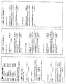
本発明の実施例を図1,図2,図3,図4,図5,図6,図7に示す。
図1は全体構成、図2,図4は本発明の実施例のハードウェア(並列と直列)、図3は本発明の実施例のハードウェア・並列・タイミングチャート、図5は本発明の実施例のハードウェア・直列・タイミングチャート、図6は本発明の実施例のソフトウェア(C言語の場合)、図7は本発明によるトレース状態出力のそれぞれ例である。
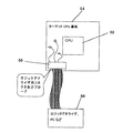
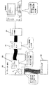
図1に示すように、本発明によるデバッグ環境の構成は非常に簡単であり、ターゲットCPU基板54側ではプログラムの処理部分毎に予め割り振ったデータを外部に出力し、この出力をコネクタ及びプローブ55を介して外部のロジックアナライザ56ないしデジタル入力ポートを備えたPC等にて記録するだけである。
並列データを入力して記録し、別途読み出しする手段があればロジックアナライザ56やPCには限定されない。
Embodiments of the present invention are shown in FIGS. 1, 2, 3, 4, 5, 6 and 7.
1 is an overall configuration, FIGS. 2 and 4 are hardware (parallel and serial) according to an embodiment of the present invention, FIG. 3 is a hardware / parallel / timing chart according to an embodiment of the present invention, and FIG. 5 is an embodiment of the present invention. FIG. 6 is an example of software (in the case of C language) according to an embodiment of the present invention, and FIG. 7 is an example of trace status output according to the present invention.
As shown in FIG. 1, the configuration of the debugging environment according to the present invention is very simple. On the
The
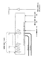
図2,図3は本発明のハードウェア部分の実施例である。この実施例ではデータをnビット(nは整数)の並列出力としているが、端子の都合で図4,図6のように直列出力としても構わない。
ただし直列出力の場合には、並列の場合よりも出力に時間がかかるため、出力データの変化する時間間隔が直列出力に要する時間よりも短い場合には利用できない。
2 and 3 show an embodiment of the hardware part of the present invention. In this embodiment, data is output in parallel with n bits (n is an integer), but may be output in series as shown in FIGS.
However, in the case of serial output, it takes longer time to output than in the case of parallel, so it cannot be used when the time interval at which the output data changes is shorter than the time required for serial output.
<並列出力の場合>
図2において、出力状態が読み出し可能なnビットレジスタの出力のポートPPOUTは、CPUが生成する書き込み信号/WRと読み出し信号/RD、及びアドレスバス信号などから生成されるデバイス選択信号/CSによって制御される。PPOUTとCPUとのデータ交換はデータバスを介して行われるものとする。これらの制御信号はCPUアーキテクチャに依存するので、必ずしもこの構成でなくても良い。
ラッチクロックLCKはCPUクロックに同期した一定周波数のクロック信号を仮定する。一般にはCPUクロックを分周してこのようなクロックを容易に得ることが可能である。
PPOUTは、CSがロウレベルになることにより、書き込みまたは読み出し可能になるものとする。
PPOUTにデータを書き込む際には、CSをロウとしておき、WRの立ち上がりでデータバスからの入力を確定する。
PPOUTからデータを読み出す際には、CSをロウとしておき、RDをロウとすることでデータバスにデータを出力する。
<For parallel output>
In FIG. 2, an output port PPOUT of an n-bit register whose output state can be read is controlled by a device selection signal / CS generated from a write signal / WR and a read signal / RD generated by the CPU, an address bus signal, and the like. Is done. Data exchange between PPOUT and the CPU is assumed to be performed via a data bus. Since these control signals depend on the CPU architecture, this configuration is not necessarily required.
The latch clock LCK is assumed to be a constant frequency clock signal synchronized with the CPU clock. In general, it is possible to easily obtain such a clock by dividing the CPU clock.
PPOUT is assumed to be writable or readable when CS goes low.
When writing data to PPOUT, CS is set low and the input from the data bus is determined at the rising edge of WR.
When reading data from PPOUT, CS is set low and data is output to the data bus by setting RD low.
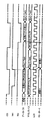
図3はこれらのタイミングチャートの概念図を示す。制御信号の極性やタイミングなどの物理的な関係はCPUのアーキテクチャに依存するため、図2,図3は概念を示している。
PPOUTの出力は外部機器で容易に読み取ることができる。ロジックアナライザを用いると、LCKを用いなくても予め設定したサンプリング間隔でPPOUTの出力を記録することができる。
ロジックアナライザ以外の手段で出力データを保存するための便宜のために、LCKが用意される。例えば、LCKの立ち上がりで出力データをラッチすることができる。LCKは、また、時間の経過を外部に伝える役割も果たすことができる。例えば、外部機器でLCKをカウンタのクロック入力に接続しておき、出力データの変化点でカウンタの値を記録することにより,プログラムの所定の範囲にどれだけ時間を要したかを容易に推定することができる。
FIG. 3 is a conceptual diagram of these timing charts. Since the physical relationship such as the polarity and timing of the control signal depends on the architecture of the CPU, FIGS. 2 and 3 show the concept.
The output of PPOUT can be easily read by an external device. If a logic analyzer is used, the output of PPOUT can be recorded at a preset sampling interval without using LCK.
The LCK is prepared for the convenience of storing the output data by means other than the logic analyzer. For example, output data can be latched at the rising edge of LCK. The LCK can also play a role of communicating the passage of time to the outside. For example, by connecting the LCK to the clock input of the counter with an external device and recording the counter value at the change point of the output data, it is possible to easily estimate how much time is required for a predetermined range of the program. be able to.
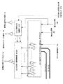
<直列出力の場合>
図4に示すように、直列出力の場合にはPPOUT出力を入力とする並列−直列変換器SPCNVとnビット直列出力制御部SCNTによって並列データを直列に変換して外部に出力する。
図5はそのタイミングチャートである。CPUとPPOUTの関係は、図2,図3と同じである。
PPOUTに書き込まれた並列データは、SCNT内において、WRをSCKを用いて遅延させて生成するラッチ信号/LDによって、SPCNVにロードされる。
SPCNVにラッチされているデータは、直列出力用のクロックScによってSPCNV内で順次シフトされつつSoとして出力される。
直列変換された信号Soを外部で受け取る便宜のために直列出力イネーブル信号/Seを用意し、/Seがロウレベルのときに直列出力データSoを外部で受け取れるようにする。
図2,図4に示すハードウェアは、汎用デバイスを用いて容易に構成することが可能であるため、ここでは詳細な説明はしない。
<For serial output>
As shown in FIG. 4, in the case of serial output, parallel data is converted into serial data by a parallel-serial converter SPCNV that receives PPOUT output and an n-bit serial output control unit SCNT, and is output to the outside.
FIG. 5 is a timing chart thereof. The relationship between the CPU and PPOUT is the same as in FIGS.
The parallel data written to PPOUT is loaded into SPCNV by a latch signal / LD generated by delaying WR using SCK in SCNT.
The data latched in the SPCNV is outputted as So while being sequentially shifted in the SPCNV by the serial output clock Sc.
For the convenience of receiving the serially converted signal So externally, a serial output enable signal / Se is prepared, and serial output data So can be received externally when / Se is at a low level.
The hardware shown in FIGS. 2 and 4 can be easily configured by using a general-purpose device, and therefore will not be described in detail here.
<ソフトウェア>
本発明においては、図2,図4などに示す簡単なハードウェアとともに、極く僅かなソフトウェア上の構成が必要である。
図6は7個の関数プログラムで本発明を説明する為のC言語のソースプログラムの一例であるが、本発明は言語仕様に依存しないので、他の言語で記述されていても同じ考え方を適用することができる。
図6において、“#define”で開始される行は、本発明において用いる、プログラムの実行部分を示す定数と、図2,図4においてPPOUTとして示すポートのI/Oアドレスの定義である。
<Software>
In the present invention, in addition to the simple hardware shown in FIGS.
FIG. 6 shows an example of a C language source program for explaining the present invention using seven function programs. However, since the present invention does not depend on language specifications, the same concept applies even if it is described in another language. can do.
In FIG. 6, the line starting with “#define” is a constant used to indicate the execution part of the program used in the present invention and the definition of the I / O address of the port indicated as PPOUT in FIGS. 2 and 4.
図4の例では、各関数プログラムに固有の数値としてMAIN LOOP,FUNC 1,FUNC 2, SUBFUNC 1, SUBFUNC 2, DEVDR 1, DEVDR 2を定義している。また、PPOUTのアドレスとして TRACE IOを定義している。なお、0×0001とは、16進数0001を意味する。
また“extern”で開始される行は、外部参照関数宣言である。ここではI/Oアドレス空間に配置されたI/Oポート入出力の関数 import() とoutport() を宣言している。
In the example of FIG. 4, MAIN is set as a numerical value unique to each function program. LOOP,
The line starting with “extern” is an external reference function declaration. Here, the functions import () and outport () of I / O port input / output arranged in the I / O address space are declared.
図6のプログラム構成は以下の通りである。
(1)関数main loop():無限ループを構成していて、関数func 1()と関数func 2()を呼び出す。
(2)関数func 1():関数 subfunc 1()を呼び出す。
(3)関数func 2():関数 subfunc 2()を呼び出す。
(4)関数 subfunc 1():関数 devdr 1()を呼び出す。
(5)関数 subfunc 2():関数 devdr 2()を呼び出す。
(6)関数 devdr 1():特に何もしない。
(7)関数 devdr 2():特に何もしない。
プログラム中の“/*”と“*/”で囲まれた部分はコメントである。
The program configuration of FIG. 6 is as follows.
(1) Function main loop (): Constructs an infinite loop and the function func 1 () and function func Call 2 ().
(2) Function func 1 (): Function subfunc Call 1 ().
(3) Function func 2 (): Function subfunc Call 2 ().
(4) Function subfunc 1 (): Function devdr Call 1 ().
(5) Function subfunc 2 (): Function devdr Call 2 ().
(6) Function devdr 1 (): Do nothing in particular.
(7) Function devdr 2 (): Do nothing in particular.
The part enclosed by “/ *” and “* /” in the program is a comment.
<関数main loop()>
処理Sm1,処理Sm2はこの関数の中で使うローカル変数の宣言である。
処理Sm1では符号なし整数として変数 trace out を、Sm2では符号付整数として変数f1及びf2を宣言している。
処理Sm3は無限ループ構造を示し、ループ中で処理Sm4,Sm5,Sm6,Sm7,Sm8を繰り返し実行する。
処理Sm4はPPOUTポートから現状の出力値を読み出し、 trace out に保存する。
処理Sm5はPPOUTポートに関数main loop()の実行を示す定数MAIN LOOPを出力する。
処理Sm6は関数func 1()、Sm7は関数func 2()を呼び出す。
処理Sm8は trace out に保存してあった以前のPPOUT出力状態を出力する。
<Function main loop ()>
Process Sm1 and process Sm2 are declarations of local variables used in this function.
In process Sm1, the variable trace as an unsigned integer In Sm2, variables f1 and f2 are declared as signed integers.
The process Sm3 shows an infinite loop structure, and the processes Sm4, Sm5, Sm6, Sm7, and Sm8 are repeatedly executed in the loop.
Process Sm4 reads the current output value from the PPOUT port, trace Save to out.
Process Sm5 is a function main at the PPOUT port. Constant MAIN indicating execution of loop () Output LOOP.
Process Sm6 is function func 1 (), Sm7 is the function func Call 2 ().
Process Sm8 is trace The previous PPOUT output state saved in out is output.
<関数func 1()とfunc 2()>
処理Sf11、処理Sf12、Sf21、Sf22、はこの関数の中で使うローカル変数の宣言である。
処理Sf11,Sf21では符号なし整数として変数 trace out を、Sf12,Sf22では符号整数として変数sbf を宣言している。
処理Sf13,Sf23はPPOUTポートから現状の出力値を読み出し、 trace out に保存する。
処理Sf14,Sf24はPPOUTポートに関数func 1()ないしfunc 2()の実行を示す定数FUNC 1またはFUNC 2を出力する。
処理Sf15は関数 subfunc 1()、Sf25は関数 subfunc 2()を呼び出す。
処理Sf16,Sf26は trace out に保存してあったもの以前のPPOUT出力状態を出力する。
処理Sf17,Sf27は戻り値としてsbf の値を持ってこの関数を抜けることを表す。
<Function func 1 () and func 2 ()>
Processes Sf11, Sf12, Sf21, and Sf22 are declarations of local variables used in this function.
In processing Sf11 and Sf21, the variable trace is set as an unsigned integer. In Sf12 and Sf22, the variable sbf is declared as a sign integer.
Processes Sf13 and Sf23 read the current output value from the PPOUT port, trace Save to out.
Processes Sf14 and Sf24 are set to function func at the PPOUT port. 1 () or func Constant FUNC indicating execution of 2 () 1 or
Process Sf15 is a function subfunc. 1 (), Sf25 is a function subfunc Call 2 ().
Processes Sf16 and Sf26 are trace Outputs the previous PPOUT output state stored in out.
Processes Sf17 and Sf27 represent exiting this function with the value of sbf as a return value.
<関数 subfunc 1()と subfunc 2()>
処理Ssf11,処理Ssf12,Ssf21,Ssf22はこの関数の中で使うローカル変数の宣言である。
処理Ssf11,Ssf21では符号なし整数として変数 trace out を、処理Ssf12,Ssf22では符号付整数として変数 devdr stを宣言している。
処理Ssf13,Ssf23はPPOUTポートから現状の出力値を読み出し、 trace out に保存する。
処理Ssf14,Ssf24はPPOUTポートに関数 subfunc 1()ないし subfunc 2()の実行を示す定数 SUBFUNC 1または SUBFUNC 2を出力する。
処理Ssf15は関数 devdr 1()、Ssf25は関数 devdr 2()を呼び出す。
処理Ssf16,Ssf26は trace out に保存してあったもの以前のPPOUT出力状態を出力する。
処理Ssf17,Ssf27は戻り値として devdr stの値を持ってこの関数を抜けることを表す。
<Function subfunc 1 () and subfunc 2 ()>
Processing Ssf11, processing Ssf12, Ssf21, and Ssf22 are declarations of local variables used in this function.
In processing Ssf11 and Ssf21, the variable trace is set as an unsigned integer. out is changed to a variable devdr as a signed integer in the processes Ssf12 and Ssf22. st is declared.
Processes Ssf13 and Ssf23 read the current output value from the PPOUT port, trace Save to out.
Processes Ssf14 and Ssf24 are set to function subfunc at the PPOUT port. 1 () or subfunc Constant indicating execution of 2 ()
The process Ssf15 is a function devdr 1 (), Ssf25 is the function devdr Call 2 ().
Processes Ssf16 and Ssf26 are trace Outputs the previous PPOUT output state stored in out.
Processes Ssf17 and Ssf27 return devdr Represents exiting this function with a value of st.
<関数 devdr 1()と devdr 2()>
処理Sd11,処理Sd21はこの関数の中で使うローカル変数の宣言である。
処理Sd11,処理Sd21では符号なし整数として変数 trace out を宣言している。
処理Sd12,処理Sd22はPPOUTポートから現状の出力値を読み出し、 trace out に保存する。
処理Sd13,処理Sd23はPPOUTポートに関数 devdr 1()ないし devdr 2()の実行を示す定数 DEVDR 1または DEVDR 2を出力する。
処理Sd14,処理Sd24は trace out に保存してあったもの以前のPPOUT出力状態を出力する。
処理Sd15,処理Sd25は戻り値として“1”ないし“2”の値を持ってこの関数を抜けることを表す。
<Function devdr 1 () and devdr 2 ()>
Process Sd11 and process Sd21 are declarations of local variables used in this function.
In process Sd11 and process Sd21, the variable trace is set as an unsigned integer. Declares out.
Process Sd12 and Process Sd22 read the current output value from the PPOUT port, trace Save to out.
Process Sd13 and process Sd23 are functions devdr at the PPOUT port. 1 () or devdr Constant DEVDR indicating execution of 2 () 1 or
Process Sd14 and process Sd24 are trace Outputs the previous PPOUT output state stored in out.
Process Sd15 and process Sd25 have a value of “1” or “2” as a return value, and indicate that this function is exited.
図6のプログラムを実行すると、時間経過に伴い、図7に示すようなPPOUT出力が得られる。
図6のプログラムは動作を説明するために記述したもので、特に実効的な処理を何も含んでいない。実際には例えば処理Sm5とSm8の間には何らかの処理が通常は記述される。
When the program of FIG. 6 is executed, a PPOUT output as shown in FIG. 7 is obtained with the passage of time.
The program in FIG. 6 is described for explaining the operation, and does not include any particularly effective processing. In practice, for example, some process is usually described between the processes Sm5 and Sm8.
本発明においてソフトウェア上で必要なことは、トレースしたい処理の先頭でPPOUTに個別データを出力することである。ソフトウェア処理は通常は図6のように入れ子構造になるので、トレースしたい処理を終えたところで以前の出力状態に戻してやる方がデバッグはしやすい。
一般的に、PPOUTのようなI/Oデバイス入出力の処理(図6では外部参照関数とした)は非常に短い処理であり、アセンブリ言語でも1行か2行で記述可能である。図6では関数呼出しで宣言しているが、コンパイラ処理でインラインアセンブリ言語のマイクロとして処理される事も多い。
アセンブリ言語で1行から2行の処理は、特殊な命令でなければ、全体の処理には全く影響を与えない場合が大半であり、割り込み処理中に記述しても多くの場合は問題がない。
一般的にデバッグ時には条件付コンパイル等を行い、デバッグの便宜のために生成コードの最適化オプションも設定しないが、本発明はそもそも簡易的なバッグ手段であることと、本来の処理に直接影響しない部分にコード生成されることが明らかであるため、最適化を行っても影響はない。
本発明ではプログラムの実行・停止を制御することはできず、トレースのみの機能しかないが、最小限のリソースで運用状態でも実時間トレースが可能である。
In the present invention, what is necessary on the software is to output individual data to PPOUT at the beginning of the process to be traced. Since software processing normally has a nested structure as shown in FIG. 6, it is easier to debug when returning to the previous output state after finishing the processing to be traced.
In general, an I / O device input / output process such as PPOUT (external reference function in FIG. 6) is a very short process, and can be described in one or two lines even in assembly language. In FIG. 6, the function call is declared, but in many cases, it is processed as a micro of an inline assembly language by compiler processing.
In the assembly language, processing from one to two lines is usually not affected at all unless it is a special instruction. In many cases, there is no problem even if it is described during interrupt processing. .
Generally, conditional compilation is performed during debugging, and the optimization option of generated code is not set for the convenience of debugging. However, the present invention is a simple bag means in the first place and does not directly affect the original processing. Since it is clear that code is generated in the part, there is no influence even if optimization is performed.
In the present invention, execution / stop of a program cannot be controlled and only a function of tracing is provided, but real-time tracing is possible even in an operating state with a minimum of resources.
システムLSI,マイクロコンピュータMPU,DPS等のプログラム制御によって動作するターゲット機器のデバッグを効率よく実施することができる。 It is possible to efficiently debug a target device that operates under program control such as a system LSI, microcomputer MPU, or DPS.
50 エミュレータ本体
51 エミュレーションポッド
52 エミュレーションプローブ
53 パソコン(PC)
54 ターゲット(CPU基板)
55 コネクタ及びプローブ
56 ロジックアナライザ(PCなど)
50
54 Target (CPU board)
55 Connector and probe 56 Logic analyzer (PC etc.)
Claims (1)
数行程度の簡単なプログラムの如きデバッグ用データ出力プログラムを前記ターゲット機器に対する所望のプログラムに含ませて動作させることにより、
前記出力端子からデバッグ用のデータが出力されるようにした
プログラム制御によって動作する機器の簡易デバッグ方式。 Equipped with an output terminal that outputs debug data from the target device,
By operating a debug data output program such as a simple program of several lines in a desired program for the target device,
A simple debugging method for a device that operates under program control in which debugging data is output from the output terminal.
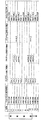
Priority Applications (1)
| Application Number | Priority Date | Filing Date | Title |
|---|---|---|---|
| JP2004104064A JP2005292978A (en) | 2004-03-31 | 2004-03-31 | Simple debugging method for devices that operate under program control |
Applications Claiming Priority (1)
| Application Number | Priority Date | Filing Date | Title |
|---|---|---|---|
| JP2004104064A JP2005292978A (en) | 2004-03-31 | 2004-03-31 | Simple debugging method for devices that operate under program control |
Publications (1)
| Publication Number | Publication Date |
|---|---|
| JP2005292978A true JP2005292978A (en) | 2005-10-20 |
Family
ID=35325873
Family Applications (1)
| Application Number | Title | Priority Date | Filing Date |
|---|---|---|---|
| JP2004104064A Pending JP2005292978A (en) | 2004-03-31 | 2004-03-31 | Simple debugging method for devices that operate under program control |
Country Status (1)
| Country | Link |
|---|---|
| JP (1) | JP2005292978A (en) |
Cited By (1)
| Publication number | Priority date | Publication date | Assignee | Title |
|---|---|---|---|---|
| CN101540706B (en) * | 2009-04-23 | 2011-12-28 | 中兴通讯股份有限公司 | Method and system for realizing remote debugging |
-
2004
- 2004-03-31 JP JP2004104064A patent/JP2005292978A/en active Pending
Cited By (1)
| Publication number | Priority date | Publication date | Assignee | Title |
|---|---|---|---|---|
| CN101540706B (en) * | 2009-04-23 | 2011-12-28 | 中兴通讯股份有限公司 | Method and system for realizing remote debugging |
Similar Documents
| Publication | Publication Date | Title |
|---|---|---|
| US6536031B2 (en) | Method for generating behavior model description of circuit and apparatus for logic verification | |
| US6889348B2 (en) | Tester architecture construction data generating method, tester architecture constructing method and test circuit | |
| JP2002323995A (en) | Trace circuit | |
| US6484273B1 (en) | Integrated EJTAG external bus interface | |
| US7428661B2 (en) | Test and debug processor and method | |
| JP3003782B2 (en) | Development support equipment | |
| US4636945A (en) | Microprocessor | |
| CN100487668C (en) | Regulating technology of built-in processor | |
| KR100423891B1 (en) | Microprocessor having trace module | |
| JP3300090B2 (en) | Test program execution method | |
| JP2005292978A (en) | Simple debugging method for devices that operate under program control | |
| US8612942B2 (en) | System for debugging computer program | |
| US5828859A (en) | Method and apparatus for setting the status mode of a central processing unit | |
| JP2006318412A (en) | Semiconductor device | |
| JP3745968B2 (en) | Test system, test method, test program, and computer-readable recording medium recording the test program | |
| JP2563708B2 (en) | Microprocessor device and emulator device using the same | |
| JPH08272770A (en) | Microcontroller Development System | |
| CN119201749B (en) | Embedded debugging method, device and system | |
| KR100788913B1 (en) | Pre-branch pattern generator for test systems of semiconductor devices | |
| JPH08171505A (en) | Semiconductor device | |
| CN119201750A (en) | Embedded testing method, device and system | |
| JPH0444292B2 (en) | ||
| KR200181133Y1 (en) | Central processing unit | |
| JP2009199113A (en) | Design device, design method using design device, and design program | |
| CN112198424A (en) | Test logic analysis unit in FPGA chip |