JP2005294507A - Electrolytic capacitor and its manufacturing method - Google Patents
Electrolytic capacitor and its manufacturing method Download PDFInfo
- Publication number
- JP2005294507A JP2005294507A JP2004106932A JP2004106932A JP2005294507A JP 2005294507 A JP2005294507 A JP 2005294507A JP 2004106932 A JP2004106932 A JP 2004106932A JP 2004106932 A JP2004106932 A JP 2004106932A JP 2005294507 A JP2005294507 A JP 2005294507A
- Authority
- JP
- Japan
- Prior art keywords
- layer
- electrolytic capacitor
- ptc
- treatment
- resistance
- Prior art date
- Legal status (The legal status is an assumption and is not a legal conclusion. Google has not performed a legal analysis and makes no representation as to the accuracy of the status listed.)
- Pending
Links
Images

Landscapes
- Fixed Capacitors And Capacitor Manufacturing Machines (AREA)
Abstract
Description
本発明は、固体電解質層を備えた電解コンデンサおよびその製造方法に関する。 The present invention relates to an electrolytic capacitor including a solid electrolyte layer and a method for manufacturing the same.
近年、高周波用途に適した電子部品のうちの1つとして、多様な電子機器に電解コンデンサが搭載されている。この電解コンデンサに関しては、例えば、電子機器のデジタル化、小型化および高速化が加速的に進行している情勢下において、大容量化や低インピーダンス化が要望されていると共に、動作安定性や動作信頼性の確保、ならびに高寿命化も併せて要望されている。 In recent years, electrolytic capacitors are mounted on various electronic devices as one of electronic components suitable for high-frequency applications. With regard to this electrolytic capacitor, for example, in a situation where the digitization, downsizing and speeding up of electronic devices are accelerating, there is a demand for large capacity and low impedance, as well as operational stability and operation. There is also a demand for ensuring reliability and extending the service life.
電解コンデンサの主要部(コンデンサ素子)は、例えば、弁作用金属により構成された陽極と、この陽極の表層が陽極酸化されることにより形成された酸化皮膜(誘電体層)と、電解質層と、陰極とがこの順に積層された積層構造を有している。 The main part (capacitor element) of the electrolytic capacitor includes, for example, an anode made of a valve metal, an oxide film (dielectric layer) formed by anodizing the surface layer of the anode, an electrolyte layer, The cathode has a laminated structure in which the cathode is laminated in this order.
この電解コンデンサは、主に、電解質層の種類に応じて2種類に大別される。すなわち、液体材料により構成された電解質層(電解液)を含んでコンデンサ素子が構成され、主にイオン伝導性を利用した導電機構を有する液体電解コンデンサと、錯塩や導電性高分子などの固体材料により構成された電解質層(固体電解質層)を含んでコンデンサ素子が構成され、主に電子伝導性を利用した導電機構を有する固体電解コンデンサである。これらの2種類の電解コンデンサを作動特性の安定性の観点において比較すると、例えば、液体電解コンデンサでは電解液の漏洩や蒸発に起因して作動特性が経時劣化し得るのに対して、この電解液の漏洩や蒸発に起因する作動特性の経時劣化は固体電解コンデンサでは起こり得ないため、今後主流になり得る電解コンデンサとして、最近では液体電解コンデンサに代えて固体電解コンデンサに関する研究開発が活発に進められている。この固体電解コンデンサに関する研究過程では、例えば、漏れ電流特性、インピーダンス特性ならびに耐熱特性などの一連の作動特性を考慮して、固体電解質層の主要部が二酸化マンガンや錯塩から共役系の導電性高分子に急速に移行しつつある。 This electrolytic capacitor is mainly divided into two types according to the type of the electrolyte layer. That is, a capacitor element is formed including an electrolyte layer (electrolyte) made of a liquid material, and has a conductive mechanism mainly utilizing ion conductivity, and a solid material such as a complex salt or a conductive polymer The capacitor element is configured to include the electrolyte layer (solid electrolyte layer) configured by the above, and is a solid electrolytic capacitor having a conductive mechanism mainly utilizing electronic conductivity. When these two types of electrolytic capacitors are compared in terms of stability of operating characteristics, for example, in liquid electrolytic capacitors, the operating characteristics may deteriorate over time due to leakage or evaporation of the electrolytic solution. As the electrolytic capacitors that can become the mainstream in the future are recently being actively researched and developed for solid electrolytic capacitors instead of liquid electrolytic capacitors, the deterioration of the operating characteristics due to leakage and evaporation of the liquid cannot occur with solid electrolytic capacitors. ing. In this research process on solid electrolytic capacitors, for example, considering the series of operating characteristics such as leakage current characteristics, impedance characteristics, and heat resistance characteristics, the main part of the solid electrolyte layer is composed of manganese dioxide or complex salts and conjugated conductive polymers. Is moving rapidly.
この固体電解コンデンサに関しては、特に、以下で説明する技術的背景に基づき、短絡時の発熱に起因して破壊されること(発火や燃焼を含む)を防止するために、所定の温度範囲内において温度の上昇に応じて抵抗が上昇する機能(いわゆるPTC(Positive Temperature Coefficient)機能)が要望されている。 With respect to this solid electrolytic capacitor, in particular, based on the technical background described below, in order to prevent destruction (including ignition and combustion) due to heat generation at the time of a short circuit, within a predetermined temperature range There is a demand for a function (so-called PTC (Positive Temperature Coefficient) function) in which the resistance increases with an increase in temperature.
すなわち、固体電解コンデンサは、上記したように多様な電子機器(電子回路)に搭載されており、一般に故障率が低い点において利点を有している。ところが、例えば、電子回路上のトラブルに起因して固体電解コンデンサに過電圧(定格電圧よりも大きい電圧)や逆電圧(正負が逆の電圧)が印加された場合に、それらの過電圧や逆電圧に起因して誘電体層が部分的に破損すると、陽極と固体電解質層および陰極とが意図せずに導通するため、固体電解コンデンサが短絡してしまう。この短絡が発生した場合に、固体電解コンデンサに過電流(短絡電流)が流れると、その固体電解コンデンサが発熱し、場合によっては発熱に起因して発火または燃焼することにより破壊されてしまう。 That is, the solid electrolytic capacitor is mounted on various electronic devices (electronic circuits) as described above, and generally has an advantage in that the failure rate is low. However, for example, when an overvoltage (a voltage greater than the rated voltage) or a reverse voltage (a voltage that is opposite in positive and negative) is applied to the solid electrolytic capacitor due to a problem in the electronic circuit, the overvoltage or reverse voltage When the dielectric layer is partially damaged due to this, the anode, the solid electrolyte layer, and the cathode are unintentionally conducted, and the solid electrolytic capacitor is short-circuited. When this short circuit occurs, if an overcurrent (short circuit current) flows through the solid electrolytic capacitor, the solid electrolytic capacitor generates heat, and in some cases, the solid electrolytic capacitor is destroyed by firing or burning.
この固体電解コンデンサの短絡時の発熱に起因する破壊を防止すると共に、固体電解コンデンサと共に電子回路に搭載されている回路部品の破壊も併せて防止する対策としては、例えば、固体電解コンデンサにヒューズを搭載する技術が考えられる。このヒューズを搭載した固体電解コンデンサとしては、例えば、陰極と陰極リード(通電用のリード)とがヒューズを介して電気的に接続された構成を有するものが知られている。この種の固体電解コンデンサでは、短絡時の発熱に起因してヒューズが溶解切断されることにより回路機構が遮断され、すなわち過電流の電流経路が遮断されるため、固体電解コンデンサの破壊が防止される。ところが、ヒューズを利用した固体電解コンデンサでは、そのヒューズの構造的および機構的要因に起因していくつかの問題がある。第1に、固体電解コンデンサにヒューズを搭載すると、その固体電解コンデンサの構造が複雑化かつ大型化してしまう。第2に、ヒューズは機械的強度が弱く、すなわちヒューズは取り扱いが困難なため、固体電解コンデンサの製造工程が複雑化すると共に製造歩留まりが低下してしまう。第3に、ヒューズを搭載した固体電解コンデンサでは、場合によっては信頼性の観点において不安がある。具体的には、例えば、ヒューズの周囲がモールド樹脂で強固に覆われている場合には、短絡時の発熱に起因してヒューズが溶解したとしても、そのヒューズがモールド樹脂の存在に起因して完全に切断されない可能性があるため、依然として回路機構が遮断されない場合に固体電解コンデンサが破壊されるおそれがある。したがって、固体電解コンデンサの破壊防止に関する信頼性を高めるために、ヒューズに代わる安全機構が模索されており、その安全機構としてPTC機能が要望されているのである。 As a measure to prevent destruction due to heat generation at the time of short-circuiting of this solid electrolytic capacitor and also prevent destruction of circuit components mounted on the electronic circuit together with the solid electrolytic capacitor, for example, a fuse is attached to the solid electrolytic capacitor. The technology to be installed can be considered. As a solid electrolytic capacitor equipped with this fuse, for example, a capacitor having a configuration in which a cathode and a cathode lead (a lead for energization) are electrically connected via a fuse is known. In this type of solid electrolytic capacitor, the circuit mechanism is cut off by melting and cutting the fuse due to heat generation at the time of short circuit, that is, the overcurrent current path is cut off, so that destruction of the solid electrolytic capacitor is prevented. The However, a solid electrolytic capacitor using a fuse has several problems due to structural and mechanical factors of the fuse. First, when a fuse is mounted on a solid electrolytic capacitor, the structure of the solid electrolytic capacitor becomes complicated and large. Secondly, the fuse has a low mechanical strength, that is, the fuse is difficult to handle, which complicates the manufacturing process of the solid electrolytic capacitor and decreases the manufacturing yield. Thirdly, solid electrolytic capacitors equipped with fuses may be anxious in terms of reliability. Specifically, for example, when the periphery of the fuse is firmly covered with mold resin, even if the fuse is melted due to heat generation at the time of short circuit, the fuse is caused by the presence of mold resin. Since it may not be completely disconnected, the solid electrolytic capacitor may be destroyed if the circuit mechanism is still not interrupted. Therefore, in order to increase the reliability regarding prevention of destruction of the solid electrolytic capacitor, a safety mechanism replacing the fuse is being sought, and a PTC function is desired as the safety mechanism.
このPTC機能を有する電解コンデンサとしては、既にいくつかの態様を有するものが提案されている。具体的には、例えば、PTCサーミスタがコンデンサ素子に対向配置され、それらのPTCサーミスタおよびコンデンサ素子がモールド樹脂で覆われた構成を有するものが知られている(例えば、特許文献1参照。)。なお、この電解コンデンサでは、ヒューズに代わる安全機構としてPTCサーミスタが設けられているわけではない。また、例えば、コンデンサ素子の陽極(内部端子)と陽極リード(外部端子)とがPTCサーミスタ(半導体セラミック層)を介して電気的に接続された構成を有するものが知られている(例えば、特許文献2参照。)。さらに、例えば、コンデンサ素子の一方の電極(外部電極)と電極リード(金属端子)とがPTCサーミスタ(PTC機能を有する過電流・過熱保護素子)を介して電気的に接続された構成を有するものが知られている(例えば、特許文献3参照。)。一般に、PTCサーミスタは、例えば、コンデンサ素子に熱圧着されたり、あるいは導電性接着剤を介してコンデンサ素子に接着されることにより電気的に接続されている。
ところで、PTC機能を有する固体電解コンデンサの高性能化を図るためには、その固体電解コンデンサの抵抗特性を可能な限り低下させる必要がある。しかしながら、従来の電解コンデンサの製造方法では、PTCサーミスタに基づくPTC機能を利用することにより、短絡時の発熱に起因する電解コンデンサの破壊は防止されるが、例えば、電解コンデンサにPTC機能を付与するために、コンデンサ素子にPTCサーミスタを接続させた場合には、PTCサーミスタの抵抗分と共に、そのPTCサーミスタとコンデンサ素子との間の接触抵抗分だけ電解コンデンサの抵抗特性が上昇し、場合によっては固体電解コンデンサの作動性能に悪影響を与える程度まで抵抗特性が上昇し得るという問題があった。なお、電解コンデンサにPTC機能を付与するために、導電性接着剤を使用してPTCサーミスタをコンデンサ素子に接着させた場合には、PTCサーミスタをコンデンサ素子に熱圧着させた場合と比較して抵抗特性の上昇量が低くなる場合が多いため、電解コンデンサの抵抗特性が上昇することを防止する上では導電性接着剤を使用した接着手法を使用するのが好ましいが、電解コンデンサの高性能化に関して今後益々要望が高まることを考慮すれば、単に導電性接着剤を使用した場合に得られる電解コンデンサの抵抗特性は未だ十分であるとは言えない。したがって、PTC機能を利用して短絡時の発熱に起因する破壊を防止しつつ、固体電解コンデンサの高性能化を図るためには、そのPTC機能を有する固体電解コンデンサの抵抗特性を可能な限り低下させることが可能な技術の確立が急務である。 Incidentally, in order to improve the performance of a solid electrolytic capacitor having a PTC function, it is necessary to reduce the resistance characteristics of the solid electrolytic capacitor as much as possible. However, in the conventional method of manufacturing an electrolytic capacitor, the use of the PTC function based on the PTC thermistor prevents the electrolytic capacitor from being destroyed due to heat generation at the time of a short circuit. For example, the electrolytic capacitor is provided with a PTC function. Therefore, when a PTC thermistor is connected to the capacitor element, the resistance characteristic of the electrolytic capacitor increases by the contact resistance between the PTC thermistor and the capacitor element together with the resistance of the PTC thermistor. There has been a problem that the resistance characteristics can be increased to such an extent that the operating performance of the electrolytic capacitor is adversely affected. In addition, in order to give a PTC function to the electrolytic capacitor, when a PTC thermistor is bonded to the capacitor element using a conductive adhesive, the resistance is higher than that when the PTC thermistor is thermocompression bonded to the capacitor element. Since the amount of increase in the characteristics is often low, it is preferable to use a bonding method using a conductive adhesive to prevent the resistance characteristics of the electrolytic capacitor from increasing. Considering the increasing demand in the future, it cannot be said that the resistance characteristics of the electrolytic capacitor obtained by simply using a conductive adhesive are still sufficient. Therefore, in order to improve the performance of the solid electrolytic capacitor while preventing the breakdown due to the heat generated at the time of short circuit using the PTC function, the resistance characteristic of the solid electrolytic capacitor having the PTC function is reduced as much as possible. There is an urgent need to establish technologies that can be used.
本発明はかかる問題点に鑑みてなされたもので、その第1の目的は、PTC機能を有する電解コンデンサの抵抗特性を可能な限り低下させることが可能な電解コンデンサの製造方法を提供することにある。 The present invention has been made in view of such problems, and a first object thereof is to provide an electrolytic capacitor manufacturing method capable of reducing resistance characteristics of an electrolytic capacitor having a PTC function as much as possible. is there.
また、本発明の第2の目的は、可能な限り低抵抗でPTC機能が確保された電解コンデンサを提供することにある。 A second object of the present invention is to provide an electrolytic capacitor having a PTC function as low resistance as possible.
本発明に係る電解コンデンサは、第1の電極層と、誘電体層と、固体電解質層と、第2の電極層とがこの順に積層された積層構造を有するコンデンサ素子と、コンデンサ素子のうちの第2の電極層に接続され、高分子中に導電性粒子が保持されたシート状構造を有すると共に第2の電極層に近い側の第1の面および遠い側の第2の面のうちの少なくとも一方に導電性粒子を露出させるための表面処理が施されており、所定の温度範囲内において温度の上昇に応じて抵抗が上昇する抵抗制御層と、抵抗制御層に接続された電極リードとを備えたものである。 An electrolytic capacitor according to the present invention includes a capacitor element having a laminated structure in which a first electrode layer, a dielectric layer, a solid electrolyte layer, and a second electrode layer are laminated in this order, Of the first surface on the side close to the second electrode layer and the second surface on the far side, which is connected to the second electrode layer and has a sheet-like structure in which conductive particles are held in the polymer A surface treatment for exposing the conductive particles is performed on at least one of the electrodes, and a resistance control layer whose resistance increases with an increase in temperature within a predetermined temperature range; and an electrode lead connected to the resistance control layer; It is equipped with.
本発明に係る電解コンデンサでは、所定の温度範囲内において温度の上昇に応じて抵抗が上昇する機能(いわゆるPTC機能)が抵抗制御層において確保されつつ、その抵抗制御層と第2の電極層または電極リードとの間の接触抵抗が低下する。 In the electrolytic capacitor according to the present invention, the resistance control layer and the second electrode layer or the second electrode layer or the function of increasing the resistance in response to the temperature rise within a predetermined temperature range (so-called PTC function) are secured in the resistance control layer. The contact resistance with the electrode lead decreases.
本発明に係る電解コンデンサの製造方法は、第1の電極層、誘電体層、固体電解質層および第2の電極層がこの順に積層された積層構造を有するコンデンサ素子のうちの第2の電極層に、高分子中に導電性粒子が保持されたシート状構造を有すると共に所定の温度範囲内において温度の上昇に応じて抵抗が上昇する抵抗制御層を接続させる工程と、抵抗制御層に、電極リードを接続させる工程とを含み、抵抗制御層を第2の電極層および電極リードに接続させる工程が、抵抗制御層の第2の電極層に対向することとなる第1の面およびその第1の面と反対側の第2の面のうちの少なくとも一方に導電性粒子を露出させるための表面処理を施す第1の工程と、抵抗制御層を第1の面において第2の電極層に接続させる第2の工程と、抵抗制御層を第2の面において電極リードに接続させる第3の工程とを含むようにしたものである。 An electrolytic capacitor manufacturing method according to the present invention includes a first electrode layer, a dielectric layer, a solid electrolyte layer, and a second electrode layer of a capacitor element having a laminated structure in which a second electrode layer is laminated in this order. And a step of connecting a resistance control layer having a sheet-like structure in which conductive particles are held in a polymer and increasing the resistance in response to a temperature rise within a predetermined temperature range, and an electrode connected to the resistance control layer. A step of connecting the resistance control layer to the second electrode layer and the electrode lead, and a step of connecting the lead to the second electrode layer of the resistance control layer and the first surface thereof. A first step of performing a surface treatment for exposing the conductive particles on at least one of the second surfaces opposite to the first surface, and connecting the resistance control layer to the second electrode layer on the first surface Second step to be performed, and resistance control layer It is obtained to include a third step of connecting the electrode lead on the second side.
本発明に係る電解コンデンサの製造方法では、所定の温度範囲内において温度の上昇に応じて抵抗が上昇する機能(いわゆるPTC機能)を有するシート状の抵抗制御層(高分子,導電性粒子)が第2の電極層および電極リードに接続される際に、その抵抗制御層の第1の面および第2の面のうちの少なくとも一方に導電性粒子を露出させるための表面処理が施されたのち、その処理済みの抵抗制御層が第1の面において第2の電極層に接続されると共に第2の面において電極リードに接続される。抵抗制御層において導電性粒子が露出することに基づき、その抵抗制御層(導電性粒子)と第2の電極層または電極リードとの間の接触面積(電気的な接続面積)が増加するため、抵抗制御層と第2の電極層または電極リードとの間の接触抵抗が低下する。 In the method for producing an electrolytic capacitor according to the present invention, there is provided a sheet-like resistance control layer (polymer, conductive particles) having a function (so-called PTC function) in which resistance increases in response to a temperature rise within a predetermined temperature range. After being connected to the second electrode layer and the electrode lead, surface treatment for exposing the conductive particles is performed on at least one of the first surface and the second surface of the resistance control layer. The treated resistance control layer is connected to the second electrode layer on the first surface and to the electrode lead on the second surface. Based on the exposure of the conductive particles in the resistance control layer, the contact area (electrical connection area) between the resistance control layer (conductive particles) and the second electrode layer or electrode lead increases. The contact resistance between the resistance control layer and the second electrode layer or electrode lead is lowered.
特に、本発明に係る電解コンデンサでは、抵抗制御層の第1の面および第2の面のうちの少なくとも一方に、表面処理としてプラズマ処理、紫外線処理、オゾン処理およびレーザ処理のうちの少なくとも1種が施されているのが好ましい。また、抵抗制御層が第1の面において第1の導電性接着剤を介して前記第2の電極層に電気的に接続されていると共に、その抵抗制御層が第2の面において第2の導電性接着剤を介して電極リードに電気的に接続されていてもよい。なお、第1の電極層が弁作用金属を含んで構成されており、誘電体層が第1の電極層の表層が陽極酸化されることにより形成されたものであってもよい。 In particular, in the electrolytic capacitor according to the present invention, at least one of plasma treatment, ultraviolet treatment, ozone treatment, and laser treatment is performed as a surface treatment on at least one of the first surface and the second surface of the resistance control layer. Is preferably applied. Further, the resistance control layer is electrically connected to the second electrode layer via the first conductive adhesive on the first surface, and the resistance control layer is second on the second surface. It may be electrically connected to the electrode lead via a conductive adhesive. Note that the first electrode layer may include a valve metal, and the dielectric layer may be formed by anodizing the surface layer of the first electrode layer.
また、本発明に係る電解コンデンサの製造方法では、第1の工程において、抵抗制御層の第1の面および第2の面のうちの少なくとも一方に、表面処理としてプラズマ処理、紫外線処理、オゾン処理およびレーザ処理のうちの少なくとも1種を施すのが好ましい。また、第2の工程において、第1の導電性接着剤を使用して抵抗制御層を第1の面において前記第2の電極層に電気的に接続させると共に、第3の工程において、第2の導電性接着剤を使用して抵抗制御層を第2の面において電極リードに電気的に接続させるようにしてもよい。 In the method for manufacturing an electrolytic capacitor according to the present invention, in the first step, at least one of the first surface and the second surface of the resistance control layer is subjected to plasma treatment, ultraviolet treatment, ozone treatment as a surface treatment. And at least one of laser treatments is preferred. In the second step, the resistance control layer is electrically connected to the second electrode layer on the first surface by using the first conductive adhesive, and in the third step, the second conductive layer is used. The resistance control layer may be electrically connected to the electrode lead on the second surface using the conductive adhesive.
本発明に係る電解コンデンサによれば、所定の温度範囲内において温度の上昇に応じて抵抗が上昇する機能(いわゆるPTC機能)が抵抗制御層において確保されつつ、その抵抗制御層と第2の電極層または電極リードとの間の接触抵抗が低下するため、可能な限り低抵抗でPTC機能を確保することができる。 According to the electrolytic capacitor of the present invention, the resistance control layer and the second electrode are secured while the resistance control layer has a function of increasing the resistance in response to the temperature rise (so-called PTC function) within a predetermined temperature range. Since the contact resistance between the layer and the electrode lead is lowered, the PTC function can be secured with as low resistance as possible.
本発明に係る電解コンデンサの製造方法によれば、所定の温度範囲内において温度の上昇に応じて抵抗が上昇する機能(いわゆるPTC機能)を有するシート状の抵抗制御層(高分子,導電性粒子)が第2の電極層および電極リードに接続される際に、その抵抗制御層の第1の面および第2の面のうちの少なくとも一方に導電性粒子を露出させるための表面処理が施されたのち、その処理済みの抵抗制御層が第1の面において第2の電極層に接続されると共に第2の面において電極リードに接続されることに基づき、その抵抗制御層と第2の電極層または電極リードとの間の接触抵抗が低下するため、PTC機能を有する電解コンデンサの抵抗特性を可能な限り低下させることができる。 According to the method for manufacturing an electrolytic capacitor according to the present invention, a sheet-like resistance control layer (polymer, conductive particles) having a function (so-called PTC function) in which resistance increases in response to a temperature rise within a predetermined temperature range. ) Is connected to the second electrode layer and the electrode lead, a surface treatment is performed to expose the conductive particles on at least one of the first surface and the second surface of the resistance control layer. After that, the processed resistance control layer is connected to the second electrode layer on the first surface and to the electrode lead on the second surface, so that the resistance control layer and the second electrode are connected. Since the contact resistance between the layer and the electrode lead is lowered, the resistance characteristic of the electrolytic capacitor having the PTC function can be lowered as much as possible.
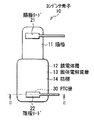
まず、図1および図2を参照して、本発明の一実施の形態に係る電解コンデンサの構成について簡単に説明する。図1および図2は電解コンデンサの構成を表しており、図1は外観構成を示し、図2は図1に示したII−II線に沿った断面構成を拡大して示している。 First, with reference to FIG. 1 and FIG. 2, the structure of the electrolytic capacitor which concerns on one embodiment of this invention is demonstrated easily. 1 and 2 show the configuration of an electrolytic capacitor, FIG. 1 shows an external configuration, and FIG. 2 shows an enlarged cross-sectional configuration along the line II-II shown in FIG.
この電解コンデンサは、例えば、図1および図2に示した、コンデンサ素子10に陽極リード21および陰極リード22が接続され、それらの陽極リード21および陰極リード22の双方が部分的に露出するようにコンデンサ素子10がモールド樹脂(図示せず)により周囲を覆われた構造を有するものである。コンデンサ素子10は、電解コンデンサの主要部として電気的反応を生じるものであり、例えば、陽極11と、この陽極11の周囲(一端部)を部分的に覆うように配設された誘電体層12と、この誘電体層12を覆うように配設された固体電解質層13と、この固体電解質層13を覆うように配設された陰極14とを含み、すなわち陽極11、誘電体層12、固体電解質層13および陰極14がこの順に積層された積層構造を有している。この電解コンデンサでは、例えば、陰極14に導電性接着剤41を介してPTC層30が接続されており、そのPTC層30に導電性接着剤42を介して陰極リード22が接続されている。
In this electrolytic capacitor, for example, the
陽極11は、拡面化(または粗面化)された表面凹凸構造を有する第1の電極層であり、例えば、アルミニウム(Al)、チタン(Ti)、タンタル(Ta)またはニオブ(Nb)などの弁作用金属を含んで構成されている。具体的には、陽極11は、例えば、アルミニウムまたはチタンなどの金属箔や、タンタルまたはニオブなどの金属焼結体である。なお、拡面化された陽極11の表面凹凸構造の詳細に関しては後述する(図3参照)。
The
誘電体層12は、例えば、弁作用金属により構成された陽極11の表層が陽極酸化されることにより形成された酸化皮膜である。この誘電体層12は、例えば、陽極11がアルミニウムより構成されている場合には、酸化アルミニウム(Al2 O3 )により構成されている。
The
固体電解質層13は、例えば、導電性高分子と、この導電性高分子の導電率を制御するためのドーパントとを含み、すなわち導電性高分子にドーパントが含有(ドープ)された構成を有している。導電性高分子は、例えば、ポリアニリン、ポリピロール、ポリチオフェン、ポリフランおよびこれらの誘導体を含む群のうちの少なくとも1種により構成されており、具体的な一例を挙げれば、ポリチオフェンの誘導体であるポリエチレンジオキシチオフェンなどにより構成されている。また、ドーパントは、例えば、アルキルベンゼンスルホン酸およびその塩、アルキルナフタレンスルホン酸およびその塩、ならびにリン酸を含む群のうちの少なくとも1種により構成されており、具体的な一例を挙げれば、パラトルエンスルホン酸鉄またはイソピロピルナフタレンスルホン酸鉄などにより構成されている。この固体電解質層13を含んでコンデンサ素子10が構成されている電解コンデンサは、いわゆる固体電解コンデンサである。
The
陰極14は、誘電体層12および固体電解質層13を挟んで陽極11に対向配置された第2の電極層である。この陰極14は、例えば、導電性を確保するための主電極層14Bと、その主電極層14Bと固体電解質層13との間に配設され、主電極層14Bを固体電解質層13に電気的に接合させるための副電極層14Aとを含み、すなわち副電極層14Aおよび主電極層14Bがこの順に積層された2層構造を有している。特に、副電極層14Aは、上記したように主電極層14Bを固体電解質層13に電気的に接合させる機能の他に、例えば、主電極層14Bを固体電解質層13に直接的に接触させた場合に、高温高湿環境中において主電極層14B中の特定成分(例えば銀(Ag))のマイグレーションを防止する機能も有している。副電極層14Aは、例えば、カーボンを含んで構成されており、主電極層14Bは、例えば、金属(例えば銀(Ag))を含んで構成されている。ただし、陽極14は必ずしも2層構造を有している必要はなく、例えば、3層以上の積層構造を有していてもよいし、あるいは単層構造を有していてもよい。
The
PTC層30は、所定の温度範囲内において温度の上昇に応じて抵抗が上昇し、より具体的には抵抗が指数関数的に上昇する機能(いわゆるPTC機能)を有する抵抗制御層である。具体的には、PTC層30は、例えば、約60℃以上150℃以下の温度範囲内において抵抗が(常温の抵抗と比較して)約1000倍以上上昇するものである。このPTC層30は、高分子中に導電性粒子が保持されたシート状構造を有しており、いわゆるポリマーPTC(P(Polymer )−PTC)層である。このPTC層30を構成する高分子は、例えば、熱硬化性高分子や熱可塑性高分子などである。具体的には、熱硬化性高分子としては、例えば、エポキシ樹脂、不飽和ポリエステル樹脂、ポリイミド、ポリウレタン、フェノール樹脂、あるいはシリコーン樹脂などが挙げられる。熱可塑性樹脂としては、例えば、オレフィン系ポリマー(例えばポリエチレン、エチレン−酢酸ビニルコポリマーまたはポリアルキルアクリレートなど)、ハロゲン系ポリマー(例えばフッ素系ポリマー(ポリフッ化ビニリデン、ポリテトラフルオロエチレン、ポリヘキサフルオロプロピレンまたはこれらのコポリマー等)または塩素系ポリマー(塩素化ポリエチレン等)など)、ポリアミド、ポリスチレン、ポリアルキレンオキサイド、あるいは熱可塑性ポリエステルなどが挙げられる。また、導電性粒子は、例えば、ニッケル(Ni)、銅(Cu)、アルミニウム(Al)、タングステン(W)、モリブデン(Mo)、亜鉛(Zn)、コバルト(Co)、白金(Pt)、金(Au)および銀(Ag)などの金属粒子、炭化タングステン(WC)、窒化チタン(TiN)、窒化ジルコニウム(ZrN)、炭化チタン(TiC)、ホウ化チタン(TiB2 )、ケイ化モリブデン(MoSi2 )およびホウ化タンタル(TaB2 )などの導電性セラミック粒子、ならびにカーボンブラック(C)などのカーボン粒子を含む群のうちの少なくとも1種である。
The
特に、シート状構造を有するPTC層30は、陰極14に近い側の下面M1(第1の面)および遠い側(陰極リード22に近い側)の上面M2(第2の面)を有しており、このPTC層30の下面M1および上面M2のうちの少なくとも一方には、導電性粒子を露出させるための表面処理が施されている。このPTC層30では、例えば、下面M1のみに表面処理が施されている。この表面処理とは、例えば、プラズマ処理、紫外線処理、オゾン処理およびレーザ処理のうちの少なくとも1種である。このPTC層30は、上記したように、下面M1において導電性接着剤41を介して陰極14に電気的に接続されていると共に、上面M2において導電性接着剤42を介して陰極リード22に電気的に接続されている。なお、表面処理が施されたPTC層30の下面M1の表面構造の詳細に関しては後述する(図4参照)。
In particular, the
導電性接着剤41は、PTC層30を陰極14に電気的に接続させるための第1の導電性接着剤であり、例えば、金属(例えば銀(Ag))を含むペースト状の接着剤である。また、導電性接着剤42は、PTC層30を陰極リード22に電気的に接続させるための第2の導電性接着剤であり、例えば、導電性接着剤31と同様の接着剤である。
The
陽極リード21および陰極リード22は、いずれもコンデンサ素子10を通電させるための電極リードである。これらの陽極リード21および陰極リード22は、例えば、いずれも鉄(Fe)または銅(Cu)などの金属や、これらの金属にめっき処理(例えば錫(Sn)めっきまたは錫鉛(SnPb)めっき)が施されためっき処理金属により構成されており、それぞれコンデンサ素子10のうちの陽極11および陰極14に接続されている。
The
なお、参考までに、モールド樹脂は、例えば、エポキシ樹脂などの絶縁性樹脂により構成されている。 For reference, the mold resin is made of an insulating resin such as an epoxy resin.
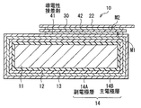
次に、図3を参照して、コンデンサ素子10の詳細な構成について説明する。図3は、図2に示したコンデンサ素子10の断面構成を部分的に拡大して表している。なお、図3では、図2に示した陰極リード22、PTC層30および導電性接着剤41,42の図示を省略している。
Next, a detailed configuration of the
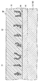
コンデンサ素子10では、例えば、図3に示したように、陽極11を覆うように誘電体層12、固体電解質層13および陰極14(副電極層14A,主電極層14B)がこの順に積層されている。このコンデンサ素子10では、陽極11の表面積を増大させることにより高容量化を実現するために、上記したように、その陽極11に拡面化処理(または粗面化処理)が施されており、すなわち陽極11が微細な表面凹凸構造を有している。この陽極11の表面凹凸構造を反映して、その陽極11を覆うように配設されている誘電体層12は微細な凹凸構造を有しており、この微細な凹凸構造を有する誘電体層12を覆うように固体電解質層13および陰極14(副電極層14A,主電極層14B)が配設されている。特に、誘電体層12は、凹凸構造のうちの凹部として複数の細孔12Hを構成しており、固体電解質層13は、誘電体層12により構成された複数の細孔12Hに部分的に入り込んでいる。
In the
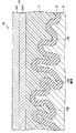
次に、図4を参照して、電解コンデンサの詳細な構成について説明する。図4は、図2に示した電解コンデンサの断面構成を部分的に拡大して表している。 Next, a detailed configuration of the electrolytic capacitor will be described with reference to FIG. FIG. 4 is a partially enlarged cross-sectional view of the electrolytic capacitor shown in FIG.
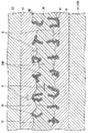
PTC層30では、上記したように、導電性粒子を露出させるための表面処理が下面M1に施されている。具体的には、例えば、図4に示したように、PTC層30の下面M1では、下面M1近傍に分布する導電性粒子31の周辺において、その導電性粒子31に沿って高分子32が部分的に除去されており、その高分子32が部分的に除去された領域として窪み30Kが形成されている。この導電性粒子31は、高分子32中において略線状に連結されており、すなわち電流経路としてのチェーン(いわゆる導電パス)を構築している。特に、PTC層30では、例えば、導電性粒子31と導電性接着剤41との間の接触面積(電気的な接続面積)を増加させることにより、そのPTC層30と陰極14との間の接触抵抗を低下させるために、除去深さDが導電性粒子31の粒径(平均粒径)Sの約1/3以上に達するまで高分子32が部分的に除去されることにより窪み30Kが形成されている。なお、図4では、高分子32中に保持されている導電性粒子31のうち、PTC層30の下面M1近傍に分布している導電性粒子31のみを示している。
As described above, the
図1〜図4に示した電解コンデンサでは、陽極リード21および陰極リード22を通じてコンデンサ素子10が通電されることにより、そのコンデンサ素子10において電荷が蓄えられる。この際、PTC機能を有するPTC層30を利用して、短絡時の発熱に起因する電解コンデンサの破壊が防止される。すなわち、例えば、電解コンデンサに過電圧や逆電圧が印加された場合に、誘電体層12が部分的に破損して短絡したことに起因して陽極11と固体電解質層13および陰極14との間に過電流が流れて発熱すると、その短絡時の発熱に基づいてPTC層30の温度が上昇することにより抵抗が指数関数的に上昇する結果、コンデンサ素子10中を流れる過電流が抑制されるため、その過電流に起因してコンデンサ素子10が破壊されにくくなる。なお、PTC層30の温度が上昇する要因としては、例えば、上記した短絡時の発熱の他に、過電流に起因するジュール熱も含まれる。こののち、PTC層30の温度が低下すると、その温度低下に応じてPTC層30の抵抗が低下するため、コンデンサ素子10が通電可能な状態に復帰する。
In the electrolytic capacitor shown in FIGS. 1 to 4, when the
なお、PTC層30がPTC機能を有する原理は、以下の通りである。すなわち、図4を参照して説明すると、温度上昇前の段階では、上記したように、PTC層30を構成している高分子32中において導電性粒子31がチェーンを構築しており、そのチェーンが高分子32により安定に保持されているため、そのチェーンの存在に基づいてPTC層30が低抵抗状態にある。しかしながら、PTC層30の温度が上昇すると、高分子32の膨張現象に起因してチェーンが切断されるため、PTC層30が高抵抗状態になる。もちろん、PTC層30の温度が低下すると、高分子32の収縮現象に基づいてチェーンが再構築されるため、PTC層30が再び低抵抗状態となる。したがって、上記したチェーンの構築・切断・再構築メカニズムを利用してPTC層30の抵抗状態が可逆的に変化可能なため、そのPTC層30がPTC機能を有するのである。
The principle that the
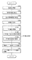
次に、図1〜図5を参照して、本発明の一実施の形態に係る電解コンデンサの製造方法として、図1〜図4に示した電解コンデンサの製造方法について説明する。図5は、電解コンデンサの製造方法に関する製造工程の流れを説明するためのものである。なお、以下では、電解コンデンサを構成する各構成要素の材質に関しては既に詳細に説明したので、その説明を随時省略するものとする。 Next, with reference to FIGS. 1-5, the manufacturing method of the electrolytic capacitor shown in FIGS. 1-4 is demonstrated as a manufacturing method of the electrolytic capacitor which concerns on one embodiment of this invention. FIG. 5 is for explaining the flow of the manufacturing process relating to the method of manufacturing the electrolytic capacitor. In addition, below, since the material of each component which comprises an electrolytic capacitor was already demonstrated in detail, the description shall be abbreviate | omitted from time to time.
電解コンデンサを製造する際には、まず、図1〜図3に示したコンデンサ素子10を形成する。すなわち、まず、陽極11として、例えば、拡面化処理が施された処理済みの弁作用金属箔(例えばアルミニウム箔やチタン箔)、すなわち微細な表面凹凸構造を有する陽極11を準備する(図5;ステップS101)。この陽極11としては、例えば、上記した拡面化処理済みの弁作用金属箔に代えて、タンタルまたはニオブなどの弁作用金属焼結体も使用可能である。なお、陽極11を準備する際には、例えば、上記したように拡面化処理済みの弁作用金属箔を使用する代わりに、未処理の弁作用金属箔を使用し、化学的または電気化学的エッチングを使用して弁作用金属箔に拡面化処理を施すことにより陽極11を形成してもよい。
When manufacturing an electrolytic capacitor, first, the
続いて、陽極11の表層を陽極酸化することにより、その陽極11の周囲を部分的に覆うように酸化皮膜よりなる誘電体層12を形成する(図5;ステップS102)。この誘電体層12としては、例えば、陽極11の形成材料としてアルミニウム箔を使用した場合には、酸化アルミニウムの皮膜により構成されるように誘電体層12を形成可能である。この誘電体層12を形成する際には、例えば、陽極11を化成溶液に浸漬させたのち、その陽極12に電圧を印加することにより陽極酸化反応を進行させるようにする。この化成溶液としては、例えば、ホウ酸アンモニウム、リン酸アンモニウムまたは有機酸アンモニウムなどを含む緩衝溶液を使用し、具体的にはアジピン酸アンモニウム水溶液などを使用する。なお、陽極11に印加する電圧は、例えば、誘電体層12の形成厚さに応じて数V〜数百Vの範囲内で自由に設定可能である。
Subsequently, the surface layer of the
続いて、誘電体層12を覆うように、ドーパントがドープされた導電性高分子を生成することにより、その導電性高分子を含むように固体電解質層13を形成する(図5;ステップS103)。この固体電解質層13を形成する際には、例えば、単量体、ドーパントおよび酸化剤を溶媒に分散させた溶液(単量体溶液)を調製し、その単量体溶液を誘電体層12の表面に塗布したのち、単量体溶液を加熱し、その単量体溶液中の酸化剤を使用して単量体を酸化重合させることにより、導電性高分子を生成する。なお、導電性高分子を生成したのちには、例えば、水、アルコール、アセトンまたはヘキサンなどを使用して導電性高分子を洗浄することにより、導電性高分子に含まれている未重合の単量体、導電性高分子にドープされなかった過剰なドーパント、ならびに使用済みの酸化剤などを洗い流して除去するのが好ましい。単量体溶液の加熱温度および加熱時間は、例えば、単量体の反応性(重合性)や酸化剤の反応性(酸化力)等を考慮して適宜設定可能である。
Subsequently, a conductive polymer doped with a dopant is formed so as to cover the
なお、単量体溶液を調整する際には、単量体として、例えば、アニリン、ピロール、チオフェン、フラン、チオフェンビニレン、イソチアナフテン、アセチレン、p−フェニレン、フェニレンビニレン、メトキシビニレン、メトキシフェニレン、フェニレンスルファイド、フェニレンオキシド、アントラセン、ナフタレン、ピレン、アズレン、セレノフェン、テルロフェンおよびこれらの誘導体を含む群のうちの少なくとも1種を使用し、具体的には3,4−エチレンジオキシチオフェンなどを使用する。 In preparing the monomer solution, examples of the monomer include aniline, pyrrole, thiophene, furan, thiophene vinylene, isothianaphthene, acetylene, p-phenylene, phenylene vinylene, methoxy vinylene, methoxy phenylene, Use at least one of the group comprising phenylene sulfide, phenylene oxide, anthracene, naphthalene, pyrene, azulene, selenophene, tellurophene and their derivatives, specifically 3,4-ethylenedioxythiophene, etc. To do.
また、ドーパントとして、例えば、ドナー型またはアクセプター型のいずれのドーパントも使用可能であり、下記の一連の材料を含む群のうちの少なくとも1種を使用する。ドナー型のドーパントとしては、例えば、リチウム(Li)、ナトリウム(Na)またはカリウム(K)などのアルカリ金属や、カルシウム(Ca)などのアルカリ土類金属等が挙げられる。一方、アクセプター型のドーパントとしては、例えば、塩素(Cl2 )、臭素(Br2 )またはヨウ素(I2 )などのハロゲンや、フッ化リン(PF3 )、フッ化ヒ素(AsF5 )またはフッ化ホウ素(BF3 )などのルイス酸や、フッ化水素(HF)、塩化水素(HCl)、硝酸(HNO3 )、硫酸(H2 SO4 )、リン酸(H3 PO4 )または過塩素酸(HClO4 )などのプロトン酸や、アルキルベンゼンスルホン酸(例えばパラトルエンスルホン酸)、アルキルナフタレンスルホン酸またはこれらの塩(例えばパラトルエンスルホン酸ナトリウムまたはアルキルナフタレンスルホン酸ナトリウム)や、塩化鉄(FeCl3 )、過塩素酸鉄(FeOCl2 )、塩化チタン(TiCl4 )または塩化タングステン(WCl3 )などの遷移金属化合物や、塩素イオン(Cl- )、臭素イオン(Br- )、ヨウ素イオン(I- )、過塩素酸イオン(ClO4 -)、フッ化リンイオン(PF3 -)、フッ化ホウ素イオン(BF3 -)またはフッ化ヒ素イオン(AsF3 -)などの電解質アニオン等が挙げられる。 In addition, as the dopant, for example, either a donor-type or acceptor-type dopant can be used, and at least one of a group including the following series of materials is used. Examples of the donor-type dopant include alkali metals such as lithium (Li), sodium (Na), and potassium (K), and alkaline earth metals such as calcium (Ca). On the other hand, examples of acceptor-type dopants include halogens such as chlorine (Cl 2 ), bromine (Br 2 ), and iodine (I 2 ), phosphorus fluoride (PF 3 ), arsenic fluoride (AsF 5 ), and fluorine. Lewis acids such as boron fluoride (BF 3 ), hydrogen fluoride (HF), hydrogen chloride (HCl), nitric acid (HNO 3 ), sulfuric acid (H 2 SO 4 ), phosphoric acid (H 3 PO 4 ) or perchlorine Protic acids such as acids (HClO 4 ), alkylbenzene sulfonic acids (eg, paratoluene sulfonic acid), alkyl naphthalene sulfonic acids or salts thereof (eg, sodium paratoluene sulfonate or sodium alkyl naphthalene sulfonate), iron chloride (FeCl 3), perchlorate (FeOCl 2), a transition such as titanium chloride (TiCl 4) or tungsten chloride (WCl 3) Or group compound, chlorine ion (Cl -), a bromine ion (Br -), iodide ion (I -), perchlorate ion (ClO 4 -), fluoride phosphorus (PF 3 -), boron fluoride ions (BF 3 − ) or electrolyte anions such as arsenic fluoride ion (AsF 3 − ).
さらに、酸化剤として、例えば、ヨウ素または臭素などのハロゲンや、五フッ化ケイ素(SiF5 )などの金属ハロゲン化物や、硫酸などのプロトン酸や、三酸化硫黄(SO3 )などの酸素化合物や、硫酸セリウム(Ce(SO4 )2 )などの硫酸塩や、過硫酸ナトリウム(Na2 S2 O8 )などの過硫酸塩や、過酸化水素(H2 O2 )などの過酸化物や、アルキルベンゼンスルホン酸塩(例えばパラトルエンスルホン酸鉄)などを使用する。 Further, as the oxidizing agent, for example, halogen such as iodine or bromine, metal halide such as silicon pentafluoride (SiF 5 ), protonic acid such as sulfuric acid, oxygen compound such as sulfur trioxide (SO 3 ), , Sulfates such as cerium sulfate (Ce (SO 4 ) 2 ), persulfates such as sodium persulfate (Na 2 S 2 O 8 ), peroxides such as hydrogen peroxide (H 2 O 2 ) Alkylbenzene sulfonate (for example, iron iron p-toluenesulfonate) is used.
なお、溶媒として、例えば、水や、ブタノールなどの有機溶媒等を使用する。 As the solvent, for example, water or an organic solvent such as butanol is used.
上記した酸化重合反応を経て生成される導電性高分子は、例えば、ポリアニリン、ポリピロール、ポリチオフェン、ポリフラン、ポリチオフェンビニレン、ポリイソチアナフテン、ポリアセチレン、ポリ−p−フェニレン、ポリフェニレンビニレン、ポリメトキシビニレン、ポリメトキシフェニレン、ポリフェニレンスルファイド、ポリフェニレンオキシド、ポリアントラセン、ポリナフタレン、ポリピレン、ポリアズレン、ポリセレノフェン、ポリテルロフェンおよびこれらの誘導体を含む群のうちの少なくとも1種であり、具体的にはポリエチレンジオキシチオフェンである。この導電性高分子としては、例えば、高分子骨格中に一次元的連鎖を有し、かつ電子供与性機能または電子受容性機能(いわゆるドーパミン機能)を有する共役系高分子が好ましい。 The conductive polymer produced through the above oxidative polymerization reaction is, for example, polyaniline, polypyrrole, polythiophene, polyfuran, polythiophene vinylene, polyisothianaphthene, polyacetylene, poly-p-phenylene, polyphenylene vinylene, polymethoxy vinylene, poly At least one member selected from the group comprising methoxyphenylene, polyphenylene sulfide, polyphenylene oxide, polyanthracene, polynaphthalene, polypyrene, polyazulene, polyselenophene, polytellurophene and their derivatives, specifically polyethylenedioxy Thiophene. As the conductive polymer, for example, a conjugated polymer having a one-dimensional chain in the polymer skeleton and having an electron donating function or an electron accepting function (so-called dopamine function) is preferable.
引き続き、電解コンデンサの製造工程について説明する。陽極11、誘電体層12および固体電解質層13がこの順に積層された積層構造を形成したのち、その固体電解質層13の周囲を覆うように、陰極14を形成する(図5;ステップS104)。この陰極14を形成する際には、例えば、固体電解質層13の周囲にカーボンペーストを塗布して乾燥させることにより副電極層14Aを形成したのち、その副電極層14A上にさらに銀ペーストを塗布して乾燥させることにより主電極層14Bを形成し、これらの副電極層14Aと主電極層14Bとがこの順に積層された積層構造を有するように陰極14を形成する。これにより、陽極11、誘電体層12、固体電解質層13および陰極14がこの順に積層された積層構造を有するコンデンサ素子10が完成する(図1〜図3参照)。
Next, the manufacturing process of the electrolytic capacitor will be described. After forming a laminated structure in which the
コンデンサ素子10を形成したのち、そのコンデンサ素子10(陰極14)に、PTC機能を有するPTC層30を接続させる(図5;ステップS105)。
After the
このPTC層30の接続手順は、例えば、以下の通りである。すなわち、まず、導電性粒子を含む高分子をシート状に成形することにより、シート状構造を有するPTC層30を準備する(ステップS1051)。続いて、PTC層30のうちの陰極14に対向することとなる下面M1およびその下面M1の反対側の上面M2のうちの少なくとも一方に、導電性粒子を露出させるための表面処理を施す(ステップS1052)。この表面処理を施す際には、例えば、PTC層30の下面M1のみに表面処理を施すようにし、その表面処理としてプラズマ処理、紫外線処理、オゾン処理およびレーザ処理のうちの少なくとも1種を施すようにする。具体的には、PTC層30の下面M1に表面処理を施すことにより、例えば、図4に示したように、導電性粒子31に沿って高分子32を部分的に除去し、その高分子32が部分的に除去された領域として窪み30Kを形成する。この場合には、特に、例えば、導電性粒子31と導電性接着剤41との間の接触面積(電気的な接続面積)を増加させることにより、PTC層30と陰極14との間の接触抵抗を低下させるために、除去深さDが導電性粒子31の粒径(平均粒径)Sの約1/3以上に達するまで高分子32を部分的に除去するのが好ましい。最後に、表面処理が施された下面M1において、導電性接着剤41を使用してPTC層30を陰極14に接着させる(ステップS1053)。これにより、PTC層30が導電性接着剤41を介して陰極14に電気的に接続される。
The connection procedure of this
なお、表面処理の手順は、例えば、以下の通りである。 The surface treatment procedure is as follows, for example.
第1に、表面処理としてプラズマ処理を使用する場合には、例えば、真空槽内に放電用ガスを導入してプラズマを発生させることにより、そのプラズマのイオン衝撃や、プラズマ中で生成される活性酸化性ガスを使用して、高分子32を部分的に除去することが可能である。この放電用ガスとしては、例えば、アルゴン(Ar)などの不活性ガスや、酸素(O2 )などの酸化性ガス、あるいはこれらの混合ガスを使用可能である。このプラズマ処理としては、具体的には、例えば、放電用ガスとして酸化性ガスを使用した反応性イオンエッチング処理や、放電ガスとして不活性ガスを使用した逆スパッタ処理などが挙げられる。
First, when plasma treatment is used as the surface treatment, for example, by introducing a discharge gas into the vacuum chamber to generate plasma, ion bombardment of the plasma or activity generated in the plasma It is possible to partially remove the
第2に、表面処理として紫外線処理を使用する場合には、例えば、紫外線を照射して高分子32中の原子間結合を切断することにより、その高分子32を部分的に除去することが可能である。この場合には、例えば、紫外線の照射処理を酸化性雰囲気中で行うことにより、高分子32を除去した際に生じる分解物を酸化性ガスで酸化除去することが可能である。また、例えば、紫外線の照射処理を不活性ガス雰囲気中で行ったのち、処理後の高分子32を水洗したり、あるいはエッチングすることによっても、その高分子23を除去した際に生じる分解物を除去することが可能である。
Second, when ultraviolet treatment is used as the surface treatment, for example, the
第3に、表面処理としてオゾン処理を使用する場合には、例えば、オゾン雰囲気中に高分子32を暴露して直接的に反応させることにより、その強力な酸化力を有するオゾンの酸化反応性を使用して高分子32を部分的に除去することが可能である。なお、例えば、紫外線処理およびオゾン処理をそれぞれ単独で使用するだけに限らず、それらの紫外線処理およびオゾン処理の双方を併用することも可能である。
Third, when ozone treatment is used as the surface treatment, for example, by exposing the
第4に、表面処理としてレーザ処理を使用する場合には、例えば、レーザ光を照射し、そのレーザ光の強力な光化学的励起反応性を使用して高分子32中の分子間結合を切断することにより、その高分子32を部分的に除去することが可能である。このレーザ処理は、一般に、レーザアブレーション法として知られており、光分解除去加工の一種である。
Fourth, when laser treatment is used as the surface treatment, for example, laser light is irradiated, and the intermolecular bond in the
なお、上記した一連の表面処理を実施するために使用する装置や処理条件などは、自由に設定可能である。 It should be noted that the apparatus and processing conditions used for carrying out the series of surface treatments described above can be freely set.
引き続き、電解コンデンサの製造工程について説明する。コンデンサ素子10にPTC層30を接続させたのち、このPTC層30が接続されたコンデンサ素子10を使用して電解コンデンサを組み立てる。すなわち、例えば、コンデンサ素子10のうちの陽極11に陽極リード21を接続させると共に、導電性接着剤42を使用してPTC層30に陰極リード22を接着させることにより、その導電性接着剤42を介して陰極リード22をPTC層30に接続させたのち(図5;ステップS106)、陽極リード21および陰極リード22の双方が部分的に露出するようにコンデンサ素子10の周囲をモールド樹脂で被覆する(図5;ステップS107)。これにより、コンデンサ素子10に陽極リード21および陰極リード22が接続され、それらの陽極リード21および陰極リード22の双方が部分的に露出するようにコンデンサ素子10がモールド樹脂により周囲を覆われた構造を有する電解コンデンサが完成する。なお、コンデンサ素子10に陽極リード21を接続させる際には、例えば、溶接処理またはかしめ加工を使用して直接的に接続させるようにしてもよいし、あるいは導電性接着剤を使用して間接的に接続させるようにしてもよい。
Next, the manufacturing process of the electrolytic capacitor will be described. After the
本実施の形態に係る電解コンデンサの製造方法では、PTC機能を有するPTC層30を陰極14に接続させるようにしたので、上記したPTC機能の原理に基づき、PTC層30により電解コンデンサにPTC機能が付与される。この場合には、特に、PTC層30の下面M1に導電性粒子を露出させるための表面処理を施したのち、その表面処理が施された下面M1においてPTC層30を陰極14に接続させたことにより、図4に示したように、PTC層30の下面M1において導電性粒子31が露出するため、図6に示したように、下面M1に表面処理を施さずにPTC層30を陰極14に接続させた場合、すなわちPTC層30の下面M1において導電性粒子31が露出していない場合と比較して、PTC層30(導電性粒子31)と陰極14との間の接触面積(電気的な接続面積)が増加するため、そのPTC層30と陰極14との間の接触抵抗が低下する。これにより、PTC機能を利用して短絡時の発熱に起因する電解コンデンサの破壊を防止しつつ、その電解コンデンサの抵抗特性を低下させることが可能となる。したがって、PTC機能を有する電解コンデンサの抵抗特性を可能な限り低下させることができる。
In the method for manufacturing an electrolytic capacitor according to the present embodiment, the
特に、本実施の形態では、導電性接着剤41を使用してPTC層30を下面M1において陰極14に接着させるようにしたので、図4に示したように、表面処理が施されることによりPTC層30の下面M1に形成された窪み30Kに導電性接着剤41が十分に入り込む。この場合には、例えば、表面処理が施されたPTC層30を下面M1において陰極14に熱圧着させた場合と比較して、導電性粒子31と導電性接着41との間の接触面積がより増加する結果、その導電性粒子31と陰極14との間の電気的な接続面積がより増加するため、PTC層30と陰極14との間の接触抵抗が著しく低下する。したがって、PTC機能を有する電解コンデンサの抵抗特性をより低下させることができる。
In particular, in the present embodiment, since the
また、本実施の形態では、図4に示したように、PTC層30の下面M1に表面処理を施すことにより高分子32を部分的に除去する際に、除去深さDが導電性粒子31の粒径(平均粒径)Sの1/3以上に達するまで高分子32を部分的に除去するようにしたので、下面M1近傍に分布している特定の導電性粒子31が窪み30Kにおいて十分に露出し、すなわちPTC層30と陰極14との間で主たる電気的な接続経路を構成する導電性粒子31の露出面積が確保される。したがって、この観点においても導電性粒子31と陰極14との間の電気的な接続面積が増加するため、PTC機能を有する電解コンデンサの抵抗特性をより低下させることができる。
In the present embodiment, as shown in FIG. 4, when the
また、上記した他、本実施の形態に係る電解コンデンサでは、PTC機能がPTC層30において確保されつつ、そのPTC層30と陰極14との間の接触抵抗が低下する。したがって、可能な限り低抵抗でPTC機能を確保することができる。
In addition to the above, in the electrolytic capacitor according to the present embodiment, the PTC function is ensured in the
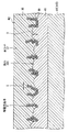
なお、本実施の形態では、PTC層30の下面M1のみに表面処理を施すようにしたが、必ずしもこれに限られるものではなく、例えば、図7および図8に示したように、PTC層30の下面M1および上面M2の双方に表面処理を施すようにしてもよい。図7は電解コンデンサの製造方法に関する変形例を説明するためのものであり、図5に対応する製造工程の流れを示している。また、図8は電解コンデンサの断面構成を部分的に拡大して表しており、図4に対応する断面構成を示している。この電解コンデンサの製造方法では、図1〜図3、図7および図8に示したように、陽極11を準備し(ステップS201)、その陽極11上に誘電体層12、固体電解質層13および陰極14を形成したのち(ステップS202,S203,S204)、その固体電解質層13に、導電性接着剤41を使用して下面M1および上面M2の双方に表面処理が施されたPTC層30を接続させる(ステップS205)。具体的には、まず、高分子中に導電性粒子が保持されたシート状のPTC層30を準備する(ステップS2051)。続いて、PTC層30の下面M1および上面M2の双方に表面処理を施すことにより(ステップS2052)、図8に示したように、下面M1および上面M2の双方において高分子32を部分的に除去して窪み30Kを形成することにより、導電性粒子31を露出させる。なお、表面処理として使用する処理の種類ならびに表面処理の手順は、例えば、上記実施の形態の場合と同様である。最後に、表面処理が施された下面M1において、導電性接着剤41を使用してPTC層30を陰極14に接着させる(ステップS2053)。これにより、PTC層30が導電性接着剤41を介して陰極14に電気的に接続される。こののち、コンデンサ素子10のうちの陽極11に陽極リード21を接続させると共に、導電性接着剤42を使用してPTC層30に陰極リード22を接着させることにより、その導電性接着剤42を介して陰極リード22をPTC層30に接続させたのち(ステップS206)、陽極リード21および陰極リード22の双方が部分的に露出するようにコンデンサ素子10の周囲をモールド樹脂で被覆することにより(ステップS207)、電解コンデンサが完成する。この場合には、上記実施の形態において説明した表面処理に基づく作用により、PTC層30の下面M1において導電性粒子31が露出するため、そのPTC層30と陰極14との間の接触抵抗が低下すると共に、上面M2においても導電性粒子31が露出するため、PTC層30と陰極リード22との間の接触抵抗も低下する。したがって、PTC層30と陰極14との間、ならびにPTC層30と陰極リード22との間の双方において接触抵抗が低下するため、PTC層30の下面M1のみに表面処理を施した上記実施の形態の場合と比較して、電解コンデンサの抵抗特性をより低下させることができる。なお、図7に示した電解コンデンサの製造方法に関する上記した以外の手順、ならびに図8に示した電解コンデンサの構成に関する上記した以外の特徴は、例えば、それぞれ図5および図4に示した場合と同様である。
In the present embodiment, only the lower surface M1 of the
もちろん、本実施の形態では、図9に示したように、PTC層30の下面M1に表面処理を施さず、上面M2のみに表面処理を施すようにしてもよい。この場合においても、PTC層30と陰極リード22との間の接触抵抗が低下することに基づき、上記実施の形態と同様の効果を得ることができる。なお、図9に示した電解コンデンサの構成に関する上記した以外の特徴は、下面M1に表面処理が施されていない点を除き、例えば、図4に示した場合と同様である。また、図9に示した電解コンデンサの製造方法は、例えば、PTC層30の下面M1に代えて上面M2に表面処理を施す点を除き、図5に示した場合と同様である。
Of course, in the present embodiment, as shown in FIG. 9, the surface treatment may be performed only on the upper surface M2 without performing the surface treatment on the lower surface M1 of the
また、本実施の形態では、PTC層30を陰極14に接続させる際に、導電性接着剤41を使用してPTC層30を陰極14に接着させるようにしたが、必ずしもこれに限られるものではなく、例えば、導電性接着剤41を使用する代わりに熱圧着などの接合手法を使用してPTC層30を陰極14に接合させるようにしてもよい。この場合においても、上記実施の形態とほぼ同様の効果を得ることができる。ただし、PTC層30を陰極14に接合させる場合には、例えば、接合時にコンデンサ素子10に過度な外力が加わると、その外力に起因して薄い誘電体層12が破損しやすいため、留意する必要がある。
In the present embodiment, when the
次に、本発明の具体的な実施例について説明する。 Next, specific examples of the present invention will be described.
上記実施の形態において説明した電解コンデンサの製造方法を使用して、電解コンデンサを製造した。すなわち、まず、陽極として処理済み(拡面化処理済み)のアルミニウム箔を準備したのち、化成溶液中においてアルミニウム箔に電圧(=23V)を印加し、陽極酸化反応を進行させて酸化アルミニウム皮膜を形成することにより、誘電体層を形成した。この誘電体層の形成後、アジピン酸アンモニウム水溶液中で容量を測定したところ、理論容量は約100μFであった。続いて、単量体、ドーパントおよび酸化剤を溶媒に分散させた単量体溶液を準備し、誘電体層を形成済みの陽極を単量体溶液に30秒間に渡って浸漬させることにより、その誘電体層の表面に単量体溶液を付着させたのち、陽極を0.5mm/秒で引き上げて室温乾燥させた。続いて、単量体溶液に浸漬済みの陽極を乾燥器に投入して加熱し、その単量体溶液に含まれている酸化剤を使用して単量体を酸化重合させることにより、ドーパントがドープされた導電性高分子を含むように固体電解質層を形成した。続いて、固体電解質層の表面にカーボンペーストを塗布して乾燥させることにより副電極層を形成し、引き続き副電極層の表面に銀ペーストを塗布して乾燥させることにより主電極層を形成し、これらの副電極層および主電極層を含む2層構造を有するように陰極を形成した。これにより、陽極、誘電体層、固体電解質層および陰極(副電極層,主電極層)がこの順に積層された積層構造を有するコンデンサ素子が形成された。続いて、導電性粒子を含む高分子をシート状に成形することによりシート状構造を有するPTC層を準備し、そのPTC層の下面(陰極に対向するととなる面)に導電性粒子を露出させるための表面処理を施したのち、導電性接着剤を使用してPTC層を下面において陰極に接着させることにより、その導電性接着剤を介してPTC層を陰極に接続させた。続いて、導電性接着剤を使用してコンデンサ素子のうちの陽極に銅製の陽極リードを接続させると共に、同様に導電性接着剤を使用してPTC層に銅製の陰極リードを接着させることにより接続させた。最後に、モールド樹脂としてエポキシ樹脂で陽極リードおよび陰極リードが部分的に露出するようにコンデンサ素子の周囲を覆うことにより、電解コンデンサが完成した。上記した導電性接着剤としては、藤倉化成株式会社製の導電性接着剤 ドータイトXA−874を使用した。 An electrolytic capacitor was manufactured using the electrolytic capacitor manufacturing method described in the above embodiment. That is, first, a treated (surface-enhanced) aluminum foil is prepared as an anode, and then a voltage (= 23 V) is applied to the aluminum foil in the chemical conversion solution to advance the anodic oxidation reaction to form an aluminum oxide film. By forming, a dielectric layer was formed. After the formation of this dielectric layer, the capacity was measured in an aqueous solution of ammonium adipate. The theoretical capacity was about 100 μF. Subsequently, a monomer solution in which a monomer, a dopant and an oxidant are dispersed in a solvent is prepared, and the anode on which the dielectric layer has been formed is immersed in the monomer solution for 30 seconds. After the monomer solution was attached to the surface of the dielectric layer, the anode was pulled up at 0.5 mm / second and dried at room temperature. Subsequently, the anode immersed in the monomer solution is put into a dryer and heated, and the dopant is oxidized by oxidative polymerization of the monomer using the oxidizing agent contained in the monomer solution. A solid electrolyte layer was formed to include the doped conductive polymer. Subsequently, a carbon paste is applied to the surface of the solid electrolyte layer and dried to form a sub-electrode layer, and subsequently a silver paste is applied to the surface of the sub-electrode layer and dried to form a main electrode layer, A cathode was formed so as to have a two-layer structure including these sub-electrode layers and main electrode layer. As a result, a capacitor element having a laminated structure in which the anode, the dielectric layer, the solid electrolyte layer, and the cathode (sub-electrode layer, main electrode layer) were laminated in this order was formed. Subsequently, a PTC layer having a sheet-like structure is prepared by forming a polymer containing conductive particles into a sheet shape, and the conductive particles are exposed on the lower surface of the PTC layer (the surface that faces the cathode). After the surface treatment was performed, the PTC layer was bonded to the cathode on the lower surface using a conductive adhesive, thereby connecting the PTC layer to the cathode via the conductive adhesive. Subsequently, the copper anode lead is connected to the anode of the capacitor element using the conductive adhesive, and the copper cathode lead is similarly bonded to the PTC layer using the conductive adhesive. I let you. Finally, an electrolytic capacitor was completed by covering the periphery of the capacitor element with an epoxy resin as a mold resin so that the anode lead and the cathode lead were partially exposed. As the conductive adhesive described above, conductive adhesive Dotite XA-874 manufactured by Fujikura Kasei Co., Ltd. was used.
なお、固体電解質層の形成手順は、以下の通りである。すなわち、まず、単量体として3,4−エチレンジオキシチオフェン(バイエル株式会社製Baytron M (商品名))、ならびにドーパント兼酸化剤としてパラトルエンスルホン酸鉄(III)50%ブタノール溶液(バイエル株式会社製Baytron C (商品名))を氷水で十分に冷却したのち、これらの単量体およびドーパント兼酸化剤をそれぞれ0.867g,10.4g秤量し、氷水で冷却しながらマグネチックスターラーで混合・攪拌することにより単量体溶液を調製した。続いて、誘電体層を形成済みの陽極を上記した浸漬条件で単量体溶液に浸漬させることにより、その誘電体層の表面に単量体溶液を付着させた。続いて、単量体溶液が付着された誘電体層を室温下において1時間程度放置したのち、その単量体溶液を加熱して単量体を酸化重合させることにより、誘電体層を覆うように導電性高分子としてポリエチレンジオキシチオフェンを生成した。この際、加熱条件は加熱温度=100℃、加熱時間=15分間とした。最後に、蒸留水を使用して導電性高分子を十分に洗浄することにより、未重合の単量体、過剰なドーパント、ならびに使用済みの酸化剤などを洗い流したのち、その導電性高分子を乾燥させた。なお、導電性高分子を形成する際には、上記した導電性高分子の生成手順を3回繰り返し、特に、酸化重合反応の完了時ごとに蒸留水やエタノールを使用して導電性高分子を洗浄することにより、未重合の単量体、余剰なドーパントならびに使用済みの酸化剤を随時除去した。これにより、導電性高分子を含む固体電解質層が形成された。 The procedure for forming the solid electrolyte layer is as follows. First, 3,4-ethylenedioxythiophene as a monomer (Baytron M (trade name) manufactured by Bayer Co., Ltd.) and 50% butanol solution of iron (III) paratoluenesulfonate as a dopant and oxidizing agent (Bayer shares) After sufficiently cooling the company's Baytron C (trade name) with ice water, weigh out 0.867 g and 10.4 g of these monomers and dopant / oxidizer, and mix them with a magnetic stirrer while cooling with ice water. -A monomer solution was prepared by stirring. Subsequently, the monomer solution was attached to the surface of the dielectric layer by immersing the anode on which the dielectric layer had been formed in the monomer solution under the immersion conditions described above. Subsequently, the dielectric layer to which the monomer solution is attached is allowed to stand at room temperature for about 1 hour, and then the monomer solution is heated to oxidatively polymerize the monomer so as to cover the dielectric layer. Polyethylenedioxythiophene was produced as a conductive polymer. At this time, the heating conditions were heating temperature = 100 ° C. and heating time = 15 minutes. Finally, the conductive polymer is thoroughly washed with distilled water to wash away unpolymerized monomers, excess dopant, used oxidant, etc., and then remove the conductive polymer. Dried. When forming the conductive polymer, the above-mentioned procedure for generating the conductive polymer is repeated three times. In particular, the conductive polymer is prepared using distilled water or ethanol every time the oxidative polymerization reaction is completed. By washing, unpolymerized monomer, excess dopant and used oxidizing agent were removed as needed. Thereby, a solid electrolyte layer containing a conductive polymer was formed.
上記した電解コンデンサの製造方法を使用して、PTC機能を有するPTC層の構成を以下のように変化させながら本発明の電解コンデンサ(実施例1〜5)を製造したのち、各電解コンデンサの諸特性を調べた。なお、本発明の電解コンデンサの諸特性を調べる際には、その性能を比較評価するために、PTC層の構成を以下のように変化させながら比較例の電解コンデンサ(比較例1〜4)を製造すると共に、参考までにPTC層を備えないように電解コンデンサ(比較例5)を製造し、各電解コンデンサの諸特性も併せて調べた。 Using the electrolytic capacitor manufacturing method described above, the electrolytic capacitor (Examples 1 to 5) of the present invention was manufactured while changing the configuration of the PTC layer having the PTC function as follows. The characteristics were investigated. When investigating the characteristics of the electrolytic capacitor of the present invention, the comparative electrolytic capacitors (Comparative Examples 1 to 4) were prepared while changing the configuration of the PTC layer as follows in order to compare and evaluate the performance. While being manufactured, an electrolytic capacitor (Comparative Example 5) was manufactured so as not to have a PTC layer for reference, and various characteristics of each electrolytic capacitor were also examined.
(実施例1)
以下の手順を経てPTC層を形成すると共にそのPTC層に表面処理を施すことにより、電解コンデンサを製造した。すなわち、PTC層の準備手順として、高分子として大日本インキ化学工業株式会社製のエポキシ樹脂 EPICLON850(エポキシ当量=190g/eq)と旭電化工業株式会社製のエポキシ樹脂 EP4005(エポキシ当量=510g/eq)との混合物(配合重量比(EPICLON850:EP4005)=75:25)を使用すると共に、導電性粒子として金属粒子、具体的にはINCO Limited社製のフィラメント状ニッケルパウダ(Ni) Type255(Niα;平均粒径=2.2μm〜2.8μm,見かけ密度=0.50g/cm3 〜0.65g/cm3 ,比表面積=0.68m2 /g,添加重量比(高分子:導電性粒子)=40:60)を使用し、高分子および導電性粒子を混合攪拌してPET(polyethylene terephthalate)フィルムの表面に塗布したのち、その塗布物を窒素雰囲気下において130℃で加熱硬化させることにより、0.2mmの厚さとなるようにシート状のPTC層を形成した。なお、PTC層の形成材料としては、上記した高分子および導電性粒子と共に、硬化補助剤として、大日本インキ化学工業株式会社製の硬化剤 B570(酸無水物当量=168g/eq,液状高分子に対して当量比=1:1)と、味の素ファインテクノ株式会社製の硬化促進剤 PN−40J(添加量=液状高分子の重量に対して1重量%)とを含むものを使用した。また、PTC層に表面処理としてオゾン処理を施し、具体的には株式会社オーク製作所製のUVオゾンクリーナ VUM−3073−13−00を使用し、オゾン雰囲気中においてPTC層の下面に3分間に渡って紫外線を照射することにより、除去深さが約5μmとなるように高分子を部分的に除去して窪みを形成した。
(Example 1)
An electrolytic capacitor was manufactured by forming a PTC layer through the following procedure and subjecting the PTC layer to a surface treatment. That is, as a preparation procedure of the PTC layer, as a polymer, epoxy resin EPICLON 850 (epoxy equivalent = 190 g / eq) manufactured by Dainippon Ink and Chemicals, and epoxy resin EP4005 (epoxy equivalent = 510 g / eq) manufactured by Asahi Denka Kogyo Co., Ltd. ) (Mixing weight ratio (EPICLON 850: EP4005) = 75: 25) and metal particles as conductive particles, specifically, filamentary nickel powder (Ni) Type 255 (Niα; manufactured by INCO Limited). Average particle size = 2.2 μm to 2.8 μm, apparent density = 0.50 g / cm 3 to 0.65 g / cm 3 , specific surface area = 0.68 m 2 / g, added weight ratio (polymer: conductive particles) = 40:60), and polymer and conductive particles are mixed and stirred to fill the PET (polyethylene terephthalate) film. It was coated on the surface of, by heat curing the coated material at 130 ° C. under a nitrogen atmosphere to form a sheet-like PTC layer so as to have a thickness of 0.2 mm. In addition, as a forming material of the PTC layer, together with the above-described polymer and conductive particles, a curing agent B570 manufactured by Dainippon Ink Chemical Co., Ltd. (acid anhydride equivalent = 168 g / eq, liquid polymer) Equivalent ratio = 1: 1) and a curing accelerator PN-40J manufactured by Ajinomoto Fine Techno Co., Ltd. (addition amount = 1 wt% with respect to the weight of the liquid polymer) was used. In addition, ozone treatment is applied to the PTC layer as a surface treatment. Specifically, UV ozone cleaner VUM-3073-13-00 manufactured by Oak Manufacturing Co., Ltd. is used, and the lower surface of the PTC layer is applied for 3 minutes in an ozone atmosphere. By irradiating with ultraviolet rays, the polymer was partially removed so as to form a depression so that the removal depth was about 5 μm.
(実施例2)
PTC層に表面処理としてオゾン処理に代えてプラズマ処理を使用した点を除き、実施例1と同様の手順を経ることにより電解コンデンサを製造した。具体的には、放電用ガスとして酸素(O2 )を用いた反応性イオンエッチング型アッシング装置を使用し、圧力=20Pa,電力密度=0.25W/cm3,処理時間=1分間の条件でPTC層の下面をエッチングした。
(Example 2)
An electrolytic capacitor was manufactured by following the same procedure as in Example 1 except that plasma treatment was used instead of ozone treatment as the surface treatment for the PTC layer. Specifically, a reactive ion etching type ashing apparatus using oxygen (O 2 ) as a discharge gas is used, under conditions of pressure = 20 Pa, power density = 0.25 W / cm 3 , and processing time = 1 minute. The lower surface of the PTC layer was etched.
(実施例3)
高分子としてAtofina Chemicals 社製のポリフッ化ビニリデン(PVDF) Kynar7201(融点=122℃〜126℃,比重=1.88)を使用すると共に、導電性粒子として導電性セラミック粒子、具体的には日本新金属株式会社製の炭化タングステン(WC) WC−F(粒径=0.62μm,添加容量比(液状高分子:導電性粒子)=70:30)を使用し、アセトンおよびトルエンの混合溶媒に溶解させた高分子中において導電性粒子をボールミル攪拌することにより調製したペーストをPETフィルムの表面に塗布したのち、その塗布物を100℃で真空乾燥させることにより、0.2mmの厚さとなるようにシート状のPTC層を形成すると共に、紫外線の照射時間=5分間,除去深さ=2μmの条件で高分子を部分的に除去した点を除き、実施例1と同様の手順を経ることにより電解コンデンサを製造した。
(Example 3)
Polyvinylidene fluoride (PVDF) Kynar 7201 (melting point = 122 ° C. to 126 ° C., specific gravity = 1.88) manufactured by Atofina Chemicals is used as a polymer, and conductive ceramic particles, specifically, Nippon Shin Tungsten carbide (WC) WC-F (particle size = 0.62 μm, additive volume ratio (liquid polymer: conductive particles) = 70: 30) manufactured by Metal Co., Ltd. is used and dissolved in a mixed solvent of acetone and toluene. After applying the paste prepared by ball mill stirring the conductive particles in the polymer to the surface of the PET film, the coating is vacuum-dried at 100 ° C. so that the thickness becomes 0.2 mm. While forming a sheet-like PTC layer, the polymer was partially removed under the conditions of UV irradiation time = 5 minutes and removal depth = 2 μm. Except, to produce an electrolytic capacitor through the same procedure as in Example 1.
(実施例4)
高分子として日本ポリエチレン株式会社製の直鎖状低密度ポリエチレン(L−LDPE;Linear Low Dnsity Polyethylene) UJ960(融点=127℃,比重=0.921)を使用すると共に、導電性粒子として金属粒子、具体的にはINCO Limited社製のフィラメント状ニッケルパウダ(Ni) Type210(Niβ;平均粒径=0.5μm〜1.0μm,見かけ密度=0.80g/cm3 ,比表面積=1.50m2 /g〜2.00m2 /g,添加容量比(高分子:導電性粒子)=65:35)を使用し、150℃の混練ミル中で高分子および導電性粒子を加熱溶融して混練させたのち、その混練物を熱プレスすると共に100kGy(グレイ)の線量で電子線架橋させることにより、0.2mmの厚さとなるようにシート状のPTC層を形成すると共に、紫外線の照射時間=3分間,除去深さ=3μmの条件で高分子を部分的に除去した点を除き、実施例1と同様の手順を経ることにより電解コンデンサを製造した。
Example 4
A linear low density polyethylene (L-LDPE) UJ960 (melting point = 127 ° C, specific gravity = 0.921) manufactured by Nippon Polyethylene Co., Ltd. is used as the polymer, and metal particles are used as the conductive particles. Specifically, filamentous nickel powder (Ni) Type 210 manufactured by INCO Limited (Niβ; average particle size = 0.5 μm to 1.0 μm, apparent density = 0.80 g / cm 3 , specific surface area = 1.50 m 2 / g to 2.00 m 2 / g, addition volume ratio (polymer: conductive particles) = 65: 35), and the polymer and conductive particles were heated and melted and kneaded in a kneading mill at 150 ° C. After that, the kneaded product is hot-pressed and cross-linked with an electron beam at a dose of 100 kGy (gray) to form a sheet-like PTC layer having a thickness of 0.2 mm. UV irradiation time = 3 min, except that the partial removal of the polymer under the conditions of removal depth = 3 [mu] m, were produced electrolytic capacitors through the same procedure as in Example 1.
(実施例5)
高分子として日本ポリエチレン株式会社製の高密度ポリエチレン(HDPE;High Density Polyethylene ) HY540(融点=135℃,比重=0.961)を使用すると共に、導電性粒子としてカーボン粒子、具体的には東海カーボン株式会社製のカーボンブラック(CB;Carbon Black) #4500 トーカブラック(粒径=40nm,DBP給油量=168cc/100g,比表面積=58m2 /g,添加容量比(高分子:導電性粒子)=68:32)を使用し、150℃の混練ミル中で高分子および導電性粒子を加熱溶融して混練させたのち、その混練物を熱プレスすると共に100kGy(グレイ)の線量で電子線架橋させることにより、0.2mmの厚さとなるようにシート状のPTC層を形成すると共に、紫外線の照射時間=1分間,除去深さ=1μmの条件で高分子を部分的に除去した点を除き、実施例1と同様の手順を経ることにより電解コンデンサを製造した。
(Example 5)
High density polyethylene (HDPE; High Density Polyethylene) HY540 (melting point = 135 ° C, specific gravity = 0.961) manufactured by Nippon Polyethylene Co., Ltd. is used as the polymer, and carbon particles, specifically Tokai Carbon, are used as the conductive particles. Carbon Black (CB) # 4500 Toka Black (particle size = 40 nm, DBP oil supply = 168 cc / 100 g, specific surface area = 58 m 2 / g, additive capacity ratio (polymer: conductive particles) = 68:32), the polymer and conductive particles are heated and melted and kneaded in a kneading mill at 150 ° C., and the kneaded product is hot-pressed and cross-linked with an electron beam at a dose of 100 kGy (gray). As a result, a sheet-like PTC layer is formed to have a thickness of 0.2 mm, and the irradiation time of ultraviolet rays is 1 minute. Depth = except that partially remove high molecular at 1μm conditions, to produce an electrolytic capacitor through the same procedure as in Example 1.
(比較例1)
PTC層の下面に表面処理を施さないことを除き、実施例1,2と同様の手順を経ることにより電解コンデンサを製造した。
(Comparative Example 1)
An electrolytic capacitor was manufactured through the same procedure as in Examples 1 and 2 except that the surface of the PTC layer was not subjected to surface treatment.
(比較例2)
PTC層の下面に表面処理を施さないことを除き、実施例3と同様の手順を経ることにより電解コンデンサを製造した。
(Comparative Example 2)
An electrolytic capacitor was manufactured through the same procedure as in Example 3 except that the surface of the PTC layer was not subjected to surface treatment.
(比較例3)
PTC層の下面に表面処理を施さないことを除き、実施例4と同様の手順を経ることにより電解コンデンサを製造した。
(Comparative Example 3)
An electrolytic capacitor was manufactured by going through the same procedure as in Example 4 except that the lower surface of the PTC layer was not subjected to surface treatment.
(比較例4)
PTC層の下面に表面処理を施さないことを除き、実施例5と同様の手順を経ることにより電解コンデンサを製造した。
(Comparative Example 4)
An electrolytic capacitor was manufactured through the same procedure as in Example 5 except that the surface of the PTC layer was not subjected to surface treatment.
(比較例5)
参考までに、PTC層を備えず、すなわちPTC機能を有しないように電解コンデンサを製造した。
(Comparative Example 5)
For reference, an electrolytic capacitor was manufactured so as not to have a PTC layer, that is, to have no PTC function.
これらの実施例1〜5および比較例1〜5の電解コンデンサの諸特性を調べたところ、表1〜表4に示した結果が得られた。表1〜表4は電解コンデンサの諸特性を表しており、その諸特性として「ESR(Equivalent Series Resistance;等価直列抵抗,mΩ)」、「漏れ電流(μA)」および「逆電圧試験」を示している。表1〜表4のうち、表1には実施例1,2および比較例1の電解コンデンサの諸特性を示し、表2には実施3および比較例2の電解コンデンサの諸特性を示し、表3には実施例4および比較例3の電解コンデンサの諸特性を示し、表4には実施例5および比較例4の電解コンデンサの諸特性を示している。なお、参考までに、表1〜表4の全てに、比較例5の電解コンデンサの諸特性も併せて示している。「ESR」としては、インピーダンスアナライザを使用して測定した各電解コンデンサの100kHzのESR値を示している。「漏れ電流」としては、各電解コンデンサに電圧(=6.3V)を5分間に渡って印加したのちに測定した漏れ電流値を示している。「逆電圧試験」としては、各電解コンデンサに逆電圧(=60V)を印加した際に不具合(例えば発火または発煙等)が観察されたものを「NG」と示し、不具合が観察されなかったものを「OK」と示している。なお、表1〜表4には、参考までに、PTC層の材料構成(高分子,導電性粒子)と共に、PTC機能の有無、PTC層の形成手法、ならびに表面処理の内容を併せて示している。 When the characteristics of the electrolytic capacitors of Examples 1 to 5 and Comparative Examples 1 to 5 were examined, the results shown in Tables 1 to 4 were obtained. Tables 1 to 4 show the characteristics of electrolytic capacitors, including "ESR (Equivalent Series Resistance; mΩ)", "Leakage Current (μA)" and "Reverse Voltage Test". ing. Of Tables 1 to 4, Table 1 shows various characteristics of the electrolytic capacitors of Examples 1 and 2 and Comparative Example 1, and Table 2 shows various characteristics of the electrolytic capacitors of Example 3 and Comparative Example 2. 3 shows characteristics of the electrolytic capacitors of Example 4 and Comparative Example 3, and Table 4 shows characteristics of the electrolytic capacitors of Example 5 and Comparative Example 4. For reference, all the characteristics of the electrolytic capacitor of Comparative Example 5 are also shown in all of Tables 1 to 4. “ESR” indicates the 100 kHz ESR value of each electrolytic capacitor measured using an impedance analyzer. “Leakage current” indicates a leakage current value measured after applying a voltage (= 6.3 V) to each electrolytic capacitor for 5 minutes. In the “reverse voltage test”, when a reverse voltage (= 60 V) was applied to each electrolytic capacitor, a failure (eg, ignition or smoke) was observed as “NG” and no failure was observed. Is indicated as “OK”. For reference, Tables 1 to 4 also show the PTC layer material configuration (polymer, conductive particles), the presence or absence of the PTC function, the method of forming the PTC layer, and the content of the surface treatment. Yes.

表1に示した結果から判るように、PTC層に表面処理が施された実施例1,2の電解コンデンサとPTC層に表面処理が施されていない比較例1の電解コンデンサとの間で諸特性を比較したところ、PTC機能を有するPTC層を備えていることに基づき、実施例1,2の電解コンデンサおよび比較例1の電解コンデンサの双方において発火や発煙等の不具合が生じなかった。また、漏れ電流は、実施例1,2の電解コンデンサと比較例1の電解コンデンサとの間でほぼ同程度であった。しかしながら、ESRは、比較例1の電解コンデンサよりも実施例1,2の電解コンデンサにおいて低くなった。すなわち、実施例1,2の電解コンデンサでは、PTC層の下面に表面処理が施されることにより導電性粒子が露出しているため、PTC層と陰極との間の接触抵抗が低下することに基づいてESRが低下した。このことから、実施例1,2の電解コンデンサでは、ESRおよび漏れ電流の双方が抑制されると共に発火や発煙などの不具合の発生が防止され、特に、それらの電解コンデンサの抵抗特性を低下させることが可能であることが確認された。なお、参考までにPTC層を備えた実施例1,2の電解コンデンサとPTC層を備えていない比較例5の電解コンデンサとの間で諸特性を調べたところ、比較例5の電解コンデンサでは、ESRおよび漏れ電流の双方に関しては実施例1,2の電解コンデンサとほぼ同程度であったが、実施例1,2の電解コンデンサとは異なり、PTC機能を有していないために逆電圧試験で発煙が生じた。 As can be seen from the results shown in Table 1, there are various conditions between the electrolytic capacitors of Examples 1 and 2 in which the PTC layer was surface-treated and the electrolytic capacitor of Comparative Example 1 in which the PTC layer was not surface-treated. When the characteristics were compared, no troubles such as ignition and smoke occurred in both the electrolytic capacitors of Examples 1 and 2 and the electrolytic capacitor of Comparative Example 1 based on the provision of the PTC layer having the PTC function. Further, the leakage current was almost the same between the electrolytic capacitors of Examples 1 and 2 and the electrolytic capacitor of Comparative Example 1. However, the ESR was lower in the electrolytic capacitors of Examples 1 and 2 than in the electrolytic capacitor of Comparative Example 1. That is, in the electrolytic capacitors of Examples 1 and 2, since the conductive particles are exposed by performing the surface treatment on the lower surface of the PTC layer, the contact resistance between the PTC layer and the cathode is reduced. Based on this, ESR decreased. Therefore, in the electrolytic capacitors of Examples 1 and 2, both ESR and leakage current are suppressed, and the occurrence of problems such as ignition and smoke is prevented, and in particular, the resistance characteristics of these electrolytic capacitors are reduced. Is confirmed to be possible. For reference, when various characteristics were examined between the electrolytic capacitors of Examples 1 and 2 having the PTC layer and the electrolytic capacitor of Comparative Example 5 having no PTC layer, the electrolytic capacitor of Comparative Example 5 was Although both the ESR and leakage current were almost the same as those of the electrolytic capacitors of Examples 1 and 2, unlike the electrolytic capacitors of Examples 1 and 2, they did not have a PTC function. Smoke occurred.
また、表2に示した結果から判るように、PTC層に表面処理が施された実施例3の電解コンデンサとPTC層に表面処理が施されていない比較例2の電解コンデンサとの間で諸特性を比較したところ、この場合においても表1に示した結果と同様に、漏れ電流および逆電圧試験の結果は実施例3の電解コンデンサと比較例2の電解コンデンサとの間でほぼ同程度であったが、ESRは比較例2の電解コンデンサよりも実施例3の電解コンデンサにおいて低くなった。このことから、実施例3の電解コンデンサにおいても、ESRおよび漏れ電流の双方が抑制されると共に発火や発煙などの不具合の発生が防止される結果、抵抗特性を低下させることが可能であることが確認された。 Further, as can be seen from the results shown in Table 2, there are various values between the electrolytic capacitor of Example 3 in which the PTC layer was subjected to surface treatment and the electrolytic capacitor of Comparative Example 2 in which the PTC layer was not subjected to surface treatment. When the characteristics were compared, the results of the leakage current and the reverse voltage test were almost the same between the electrolytic capacitor of Example 3 and the electrolytic capacitor of Comparative Example 2 in this case as well as the results shown in Table 1. However, the ESR was lower in the electrolytic capacitor of Example 3 than in the electrolytic capacitor of Comparative Example 2. From this, also in the electrolytic capacitor of Example 3, it is possible to reduce resistance characteristics as a result of suppressing both ESR and leakage current and preventing occurrence of problems such as ignition and smoke. confirmed.
さらに、表3に示した結果から判るように、PTC層に表面処理が施された実施例4の電解コンデンサとPTC層に表面処理が施されていない比較例3の電解コンデンサとの間で諸特性を比較したところ、この場合においても表1に示した結果と同様に、漏れ電流および逆電圧試験の結果は実施例4の電解コンデンサと比較例3の電解コンデンサとの間でほぼ同程度であったが、ESRは比較例3の電解コンデンサよりも実施例4の電解コンデンサにおいて低くなった。このことから、実施例4の電解コンデンサにおいても、ESRおよび漏れ電流の双方が抑制されると共に発火や発煙などの不具合の発生が防止される結果、抵抗特性を低下させることが可能であることが確認された。 Further, as can be seen from the results shown in Table 3, various values were observed between the electrolytic capacitor of Example 4 in which the surface treatment was applied to the PTC layer and the electrolytic capacitor of Comparative Example 3 in which the surface treatment was not applied to the PTC layer. When the characteristics were compared, the results of the leakage current and the reverse voltage test were almost the same between the electrolytic capacitor of Example 4 and the electrolytic capacitor of Comparative Example 3 in this case as well as the results shown in Table 1. However, the ESR was lower in the electrolytic capacitor of Example 4 than in the electrolytic capacitor of Comparative Example 3. From this, also in the electrolytic capacitor of Example 4, it is possible to reduce resistance characteristics as a result of suppressing both ESR and leakage current and preventing occurrence of problems such as ignition and smoke. confirmed.
最後に、表4に示した結果から判るように、PTC層に表面処理が施された実施例5の電解コンデンサとPTC層に表面処理が施されていない比較例4の電解コンデンサとの間で諸特性を比較したところ、この場合においても表1に示した結果と同様に、漏れ電流および逆電圧試験の結果は実施例5の電解コンデンサと比較例4の電解コンデンサとの間でほぼ同程度であったが、ESRは比較例4の電解コンデンサよりも実施例5の電解コンデンサにおいて低くなった。このことから、実施例5の電解コンデンサにおいても、ESRおよび漏れ電流の双方が抑制されると共に発火や発煙などの不具合の発生が防止される結果、抵抗特性を低下させることが可能であることが確認された。 Finally, as can be seen from the results shown in Table 4, between the electrolytic capacitor of Example 5 where the surface treatment was applied to the PTC layer and the electrolytic capacitor of Comparative Example 4 where the surface treatment was not applied to the PTC layer. When various characteristics were compared, in this case as well, the results of the leakage current and the reverse voltage test were almost the same between the electrolytic capacitor of Example 5 and the electrolytic capacitor of Comparative Example 4 as in the results shown in Table 1. However, the ESR was lower in the electrolytic capacitor of Example 5 than in the electrolytic capacitor of Comparative Example 4. Therefore, also in the electrolytic capacitor of Example 5, both the ESR and the leakage current are suppressed, and the occurrence of problems such as ignition and smoke is prevented, so that the resistance characteristics can be lowered. confirmed.
以上説明したように、本発明(実施例1〜5)の電解コンデンサでは、いずれの場合においても抵抗特性を低下させることが可能であった。特に、本発明の電解コンデンサ間でESRを比較したところ、導電性粒子としてカーボン粒子を使用した実施例5の電解コンデンサよりも、導電性粒子として金属粒子または導電性セラミック粒子を使用した実施例1〜4の電解コンデンサにおいてESRを低下させることが可能であることが確認された。 As described above, in the electrolytic capacitors of the present invention (Examples 1 to 5), it was possible to reduce the resistance characteristics in any case. In particular, when the ESR was compared between the electrolytic capacitors of the present invention, Example 1 in which metal particles or conductive ceramic particles were used as conductive particles rather than the electrolytic capacitor in Example 5 in which carbon particles were used as conductive particles. It was confirmed that ESR can be lowered in the electrolytic capacitors of ˜4.
なお、具体的にデータを示した上で説明しないが、PTC層の下面に表面処理としてプラズマ処理およびオゾン処理に代えて紫外線処理およびレーザ処理を施して電解コンデンサを製造することにより同様に諸特性を調べたところ、いずれの電解コンデンサにおいても実施例1〜5の電解コンデンサに関して得られた結果と同様の結果が得られた。このことから、表面処理の処理内容にかかわらず、PTC層の下面に導電性粒子を露出させるための表面処理を施すことにより、電解コンデンサの抵抗特性を低下させることが可能であることが確認された。 In addition, although it does not explain after showing data concretely, various characteristics are similarly obtained by manufacturing the electrolytic capacitor by performing ultraviolet treatment and laser treatment instead of plasma treatment and ozone treatment as the surface treatment on the lower surface of the PTC layer. As a result, the same results as those obtained with respect to the electrolytic capacitors of Examples 1 to 5 were obtained in any electrolytic capacitor. From this, it was confirmed that the resistance characteristics of the electrolytic capacitor can be reduced by applying a surface treatment for exposing the conductive particles on the lower surface of the PTC layer, regardless of the treatment content of the surface treatment. It was.
また、同様に具体的にデータを示した上で説明しないが、PTC層の下面のみに表面処理が施された電解コンデンサに代えて、PTC層の上面のみに表面処理が施された電解コンデンサ、ならびにPTC層の上面および下面の双方に表面処理が施された電解コンデンサを製造することにより同様に諸特性を調べたところ、やはりいずれの電解コンデンサにおいても実施例1〜5の電解コンデンサに関して得られた結果と同様の結果が得られた。このことから、PTC層に表面処理を施すことにより、電解コンデンサの抵抗特性を低下させることが可能であることが確認された。 Similarly, although not specifically described after showing data, an electrolytic capacitor in which only the upper surface of the PTC layer is subjected to surface treatment instead of the electrolytic capacitor in which the surface treatment is performed only on the lower surface of the PTC layer, In addition, when various characteristics were similarly examined by manufacturing an electrolytic capacitor in which both the upper surface and the lower surface of the PTC layer were subjected to surface treatment, all the electrolytic capacitors were obtained with respect to the electrolytic capacitors of Examples 1 to 5. Similar results were obtained. From this, it was confirmed that the resistance characteristics of the electrolytic capacitor can be lowered by subjecting the PTC layer to a surface treatment.
参考までに、実施例1〜5および比較例1〜4のPTC層に関してPTC特性を調べたところ、表5に示した結果が得られた。表5はPTC層のPTC特性を表しており、そのPTC特性として「室温抵抗(mΩ)」、「動作開始温度(℃)」および「抵抗変化率(桁数)」を示している。この「動作開始温度」は、25℃で示した抵抗値と比較して、その抵抗値の5倍の抵抗値を示した温度である。また、「抵抗変化率」は、抵抗の上昇桁数を表しており、すなわち室温抵抗R1とPTC機能に基づいて上昇した抵抗R2との間にR2=10x ×R1の関係が成立している場合の桁数xを表している。PTC特性を調べる際には、実施例1〜3および比較例1,2に関しては、PTCの形成材料(導電性粒子を含む高分子)を2枚の電解ニッケル箔電極(25μm厚)間において0.2mmの厚さとなるように膜化することにより電極付きPTCシートを作製し、直径10mmの円盤状に打ち抜いたのち、その電極付きPTCシートを恒温槽中に投入し、25℃〜160℃の範囲内において2℃/分で昇温させながら4端子法で2℃ごとに抵抗を測定した。また、実施例4,5および比較例3,4に関しては、2枚の電解ニッケル箔電極間にPTC層を熱圧着した点を除いて実施例1〜3および実施例1,2の場合と同様の手順を経ることにより電極付きPTCシートを作製し、その電極付きPTCシートの抵抗を同条件で測定した。 For reference, the PTC characteristics of the PTC layers of Examples 1 to 5 and Comparative Examples 1 to 4 were examined. The results shown in Table 5 were obtained. Table 5 shows the PTC characteristics of the PTC layer. As the PTC characteristics, “room temperature resistance (mΩ)”, “operation start temperature (° C.)”, and “resistance change rate (number of digits)” are shown. This “operation start temperature” is a temperature indicating a resistance value five times that of the resistance value indicated at 25 ° C. Further, the “resistance change rate” represents the number of increasing digits of the resistance, that is, a relationship of R2 = 10 ×× R1 is established between the room temperature resistance R1 and the resistance R2 increased based on the PTC function. Represents the number of digits x. When examining the PTC characteristics, with respect to Examples 1 to 3 and Comparative Examples 1 and 2, the PTC forming material (polymer containing conductive particles) was zero between two electrolytic nickel foil electrodes (25 μm thick). A PTC sheet with an electrode was produced by forming a film to a thickness of 2 mm, punched into a disk shape having a diameter of 10 mm, and then the PTC sheet with an electrode was put into a thermostatic bath, and the temperature was 25 ° C. to 160 ° C. The resistance was measured every 2 ° C. by the 4-terminal method while raising the temperature at 2 ° C./min within the range. Examples 4 and 5 and Comparative Examples 3 and 4 are the same as those in Examples 1 to 3 and Examples 1 and 2, except that a PTC layer was thermocompression bonded between two electrolytic nickel foil electrodes. The PTC sheet with an electrode was produced by going through the procedure of, and the resistance of the PTC sheet with an electrode was measured under the same conditions.
表5に示した結果から判るように、実施例1〜5および比較例1〜4のPTC層では、いずれの場合においても3桁以上の抵抗変化率が得られ、すなわち抵抗が1000倍以上に上昇した。このことから、実施例1〜5および比較例1〜4のPTC層は、PTC機能を発揮し得るだけの十分な抵抗変化率を有していることが確認された。なお、具体的にデータを示した上で説明しないが、確認までに、PTC機能を有していないカーボンブラックペースト(実施例1〜5および比較例1〜4の副電極層)および同様にPTC機能を有していない銀ペースト(実施例1〜5および比較例1〜4の主電極層)の抵抗特性を調べ、具体的には、ディップ法を使用して30mm×30mm寸法のガラス板上に各ペーストを成膜(加熱・乾燥を含む)したのち、金属クリップで挟んで各ペーストの室温抵抗を測定すると共に、150℃の恒温槽中で同様に各ペーストの抵抗を測定したところ、各ペーストの抵抗の上昇率は20%以内に留まり、PTC機能を発揮し得るだけの十分な抵抗変化率が得られなかった。 As can be seen from the results shown in Table 5, the PTC layers of Examples 1 to 5 and Comparative Examples 1 to 4 can obtain a resistance change rate of 3 digits or more in any case, that is, the resistance is 1000 times or more. Rose. From this, it was confirmed that the PTC layers of Examples 1 to 5 and Comparative Examples 1 to 4 have a sufficient resistance change rate that can exhibit the PTC function. In addition, although it does not explain after showing data concretely, by the time of confirmation, carbon black paste (subelectrode layer of Examples 1-5 and Comparative Examples 1-4) which does not have a PTC function, and PTC similarly The resistance characteristics of the silver paste having no function (the main electrode layers of Examples 1 to 5 and Comparative Examples 1 to 4) were examined, specifically, on a glass plate having a size of 30 mm × 30 mm using the dip method. After each paste was formed into a film (including heating and drying), the resistance of each paste was measured in a constant temperature bath at 150 ° C. The rate of increase in the resistance of the paste remained within 20%, and a sufficient resistance change rate that could exhibit the PTC function was not obtained.
以上、実施の形態および実施例を挙げて本発明を説明したが、本発明はこれらの実施の形態や実施例に限定されず、種々の変形が可能である。具体的には、上記実施の形態および実施例では、PTC層に施す表面処理、すなわち導電性粒子を露出させるための表面処理としてプラズマ処理、紫外線処理、オゾン処理およびレーザ処理のうちの少なくとも1種を施すようにしたが、必ずしもこれに限られるものではなく、上記したように、導電性粒子を露出させることによりPTC層と陰極または陰極リード22との間の接触抵抗を低下させることが可能な限り、表面処理としては上記した一連の処理以外の他の処理を使用してもよい。この「他の処理」としては、例えば、表面凹凸構造を有する金属箔の表面にシート状構造を有するPTC層を貼り付けたのち、そのPTC層を金属箔から剥がすことにより、その金属箔の表面凹凸構造を利用してPTC層の表面を荒らす(導電性粒子が露出するように高分子を部分的に除去する)手法が挙げられる。この他の処理を使用して表面処理を行った場合においても、上記実施の形態および実施例と同様の効果を得ることができる。
While the present invention has been described with reference to the embodiments and examples, the present invention is not limited to these embodiments and examples, and various modifications can be made. Specifically, in the above-described embodiments and examples, at least one of plasma treatment, ultraviolet treatment, ozone treatment, and laser treatment is performed as the surface treatment applied to the PTC layer, that is, the surface treatment for exposing the conductive particles. However, the present invention is not necessarily limited to this. As described above, the contact resistance between the PTC layer and the cathode or
本発明に係る電解コンデンサおよびその製造方法は、電気的反応を生じる主要部(コンデンサ素子)が固体材料(導電性高分子)を含んで構成された固体電解コンデンサおよびその製造方法に適用することが可能である。 The electrolytic capacitor and the manufacturing method thereof according to the present invention can be applied to a solid electrolytic capacitor in which a main part (capacitor element) that generates an electrical reaction includes a solid material (conductive polymer) and a manufacturing method thereof. Is possible.
10…コンデンサ素子、11…陽極、12…誘電体層、12H…細孔、13…固体電解質層、14…陰極、14A…副電極層、14B…主電極層、21…陽極リード、22…陰極リード、30…PTC層、31…導電性粒子、32…高分子、41,42…導電性接着剤、D…除去深さ、M1…下面、M2…上面、S…粒径。
DESCRIPTION OF
Claims (9)
前記コンデンサ素子のうちの前記第2の電極層に接続され、高分子中に導電性粒子が保持されたシート状構造を有すると共に前記第2の電極層に近い側の第1の面および遠い側の第2の面のうちの少なくとも一方に前記導電性粒子を露出させるための表面処理が施されており、所定の温度範囲内において温度の上昇に応じて抵抗が上昇する抵抗制御層と、
前記抵抗制御層に接続された電極リードと
を備えたことを特徴とする電解コンデンサ。 A capacitor element having a laminated structure in which a first electrode layer, a dielectric layer, a solid electrolyte layer, and a second electrode layer are laminated in this order;
The capacitor element has a sheet-like structure connected to the second electrode layer, in which conductive particles are held in a polymer, and a first surface and a far side closer to the second electrode layer A surface treatment for exposing the conductive particles to at least one of the second surfaces of the resistance control layer, and a resistance control layer whose resistance increases in response to a temperature rise within a predetermined temperature range;
An electrolytic capacitor comprising: an electrode lead connected to the resistance control layer.
ことを特徴とする請求項1記載の電解コンデンサ。 At least one of plasma treatment, ultraviolet treatment, ozone treatment, and laser treatment is applied as at least one of the first surface and the second surface of the resistance control layer as the surface treatment. The electrolytic capacitor according to claim 1.
ことを特徴とする請求項1または請求項2に記載の電解コンデンサ。 The said resistance control layer is electrically connected to the said 2nd electrode layer via the 1st conductive adhesive in the said 1st surface. The Claim 1 or Claim 2 characterized by the above-mentioned. Electrolytic capacitor.
ことを特徴とする請求項1ないし請求項3のいずれか1項に記載の電解コンデンサ。 The resistance control layer is electrically connected to the electrode lead via a second conductive adhesive on the second surface. 4. The electrolytic capacitor described in 1.
前記誘電体層が、前記第1の電極層の表層が陽極酸化されることにより形成されたものである
ことを特徴とする請求項1ないし請求項4のいずれか1項に記載の電解コンデンサ。 The first electrode layer comprises a valve metal;
The electrolytic capacitor according to any one of claims 1 to 4, wherein the dielectric layer is formed by anodizing a surface layer of the first electrode layer.
前記抵抗制御層に、電極リードを接続させる工程と、を含み、
前記抵抗制御層を前記第2の電極層および前記電極リードに接続させる工程が、
前記抵抗制御層の前記第2の電極層に対向することとなる第1の面およびその第1の面と反対側の第2の面のうちの少なくとも一方に、前記導電性粒子を露出させるための表面処理を施す第1の工程と、
前記抵抗制御層を前記第1の面において前記第2の電極層に接続させる第2の工程と、
前記抵抗制御層を前記第2の面において前記電極リードに接続させる第3の工程と、を含む
ことを特徴とする電解コンデンサの製造方法。 Conductive particles in the polymer are formed on the second electrode layer of the capacitor element having a laminated structure in which the first electrode layer, the dielectric layer, the solid electrolyte layer, and the second electrode layer are laminated in this order. Connecting a resistance control layer having a held sheet-like structure and having a resistance that rises as the temperature rises within a predetermined temperature range;
A step of connecting an electrode lead to the resistance control layer,
Connecting the resistance control layer to the second electrode layer and the electrode lead;
In order to expose the conductive particles on at least one of the first surface of the resistance control layer facing the second electrode layer and the second surface opposite to the first surface. A first step of performing the surface treatment of
A second step of connecting the resistance control layer to the second electrode layer on the first surface;
And a third step of connecting the resistance control layer to the electrode lead on the second surface. A method of manufacturing an electrolytic capacitor, comprising:
ことを特徴とする請求項6記載の電解コンデンサの製造方法。 In the first step, at least one of plasma treatment, ultraviolet treatment, ozone treatment, and laser treatment as the surface treatment is performed on at least one of the first surface and the second surface of the resistance control layer. The method for producing an electrolytic capacitor according to claim 6, wherein seeding is performed.
ことを特徴とする請求項6または請求項7に記載の電解コンデンサの製造方法。 In the second step, the resistance control layer is electrically connected to the second electrode layer on the first surface by using a first conductive adhesive. The manufacturing method of the electrolytic capacitor of Claim 7.
ことを特徴とする請求項6ないし請求項8のいずれか1項に記載の電解コンデンサの製造方法。 The said 3rd process WHEREIN: The said resistance control layer is electrically connected to the said electrode lead in the said 2nd surface using a 2nd electroconductive adhesive agent, The Claim 6 thru | or 8 characterized by the above-mentioned. The manufacturing method of the electrolytic capacitor of any one of these.
Priority Applications (3)
| Application Number | Priority Date | Filing Date | Title |
|---|---|---|---|
| JP2004106932A JP2005294507A (en) | 2004-03-31 | 2004-03-31 | Electrolytic capacitor and its manufacturing method |
| US11/089,227 US7218506B2 (en) | 2004-03-31 | 2005-03-25 | Electrolytic capacitor and method of manufacturing the same |
| US11/634,126 US7245479B2 (en) | 2004-03-31 | 2006-12-06 | Electrolytic capacitor and method of manufacturing the same |
Applications Claiming Priority (1)
| Application Number | Priority Date | Filing Date | Title |
|---|---|---|---|
| JP2004106932A JP2005294507A (en) | 2004-03-31 | 2004-03-31 | Electrolytic capacitor and its manufacturing method |
Publications (1)
| Publication Number | Publication Date |
|---|---|
| JP2005294507A true JP2005294507A (en) | 2005-10-20 |
Family
ID=35327106
Family Applications (1)
| Application Number | Title | Priority Date | Filing Date |
|---|---|---|---|
| JP2004106932A Pending JP2005294507A (en) | 2004-03-31 | 2004-03-31 | Electrolytic capacitor and its manufacturing method |
Country Status (1)
| Country | Link |
|---|---|
| JP (1) | JP2005294507A (en) |
-
2004
- 2004-03-31 JP JP2004106932A patent/JP2005294507A/en active Pending
Similar Documents
| Publication | Publication Date | Title |
|---|---|---|
| US7218506B2 (en) | Electrolytic capacitor and method of manufacturing the same | |
| TWI478189B (en) | Solid electrolytic capacitor and method of manufacturing thereof | |
| JP3070408B2 (en) | Solid electrolytic capacitor and method of manufacturing the same | |
| US6999303B2 (en) | Solid electrolytic capacitor and process for its fabrication | |
| US7940515B2 (en) | Solid electrolytic capacitor | |
| CN100421192C (en) | Preparation method of solid electrolytic capacitor | |
| JP4983744B2 (en) | Manufacturing method of solid electrolytic capacitor | |
| WO2006075551A1 (en) | Solid electrolytic capacitor and method for manufacturing same | |
| JP5895227B2 (en) | Solid electrolytic capacitor and manufacturing method thereof | |
| WO2018043063A1 (en) | Electrolytic capacitor and method for producing same | |
| JPWO2013088845A1 (en) | Solid electrolytic capacitor | |
| JP3356018B2 (en) | Capacitor and manufacturing method thereof | |
| JP2005294507A (en) | Electrolytic capacitor and its manufacturing method | |
| JP4539141B2 (en) | Electrolytic capacitor and manufacturing method thereof | |
| JP2005294522A (en) | Electrolytic capacitor and its manufacturing method | |
| JP2003289015A (en) | Polymer solid electrolytic capacitor | |
| JP4937170B2 (en) | Solid electrolytic capacitor | |
| CN115621048A (en) | Solid electrolytic capacitor and method for manufacturing solid electrolytic capacitor | |
| JP4401195B2 (en) | Solid electrolytic capacitor and manufacturing method thereof | |
| JP2005294420A (en) | Electrolytic capacitor or its manufacturing method | |
| JP2005135853A (en) | Solid electrolyte, electrolytic capacitor and its manufacturing method | |
| JP4845835B2 (en) | Solid electrolytic capacitor and manufacturing method thereof | |
| JP2005136336A (en) | Solid electrolyte and its manufacturing method, and electrolytic capacitor and its manufacturing method | |
| JP2005191126A (en) | Method for forming conductive polymer, and method for producing electronic component | |
| JPH10289839A (en) | Manufacture of solid electrolytic capacitor |
Legal Events
| Date | Code | Title | Description |
|---|---|---|---|
| A621 | Written request for application examination |
Free format text: JAPANESE INTERMEDIATE CODE: A621 Effective date: 20061116 |
|
| A977 | Report on retrieval |
Free format text: JAPANESE INTERMEDIATE CODE: A971007 Effective date: 20090910 |
|
| A131 | Notification of reasons for refusal |
Free format text: JAPANESE INTERMEDIATE CODE: A131 Effective date: 20090917 |
|
| A02 | Decision of refusal |
Free format text: JAPANESE INTERMEDIATE CODE: A02 Effective date: 20100126 |