JP2005294533A - 半導体装置 - Google Patents
半導体装置 Download PDFInfo
- Publication number
- JP2005294533A JP2005294533A JP2004107544A JP2004107544A JP2005294533A JP 2005294533 A JP2005294533 A JP 2005294533A JP 2004107544 A JP2004107544 A JP 2004107544A JP 2004107544 A JP2004107544 A JP 2004107544A JP 2005294533 A JP2005294533 A JP 2005294533A
- Authority
- JP
- Japan
- Prior art keywords
- region
- active layer
- main electrode
- disposed
- insulating film
- Prior art date
- Legal status (The legal status is an assumption and is not a legal conclusion. Google has not performed a legal analysis and makes no representation as to the accuracy of the status listed.)
- Granted
Links
Images



Classifications
-
- H—ELECTRICITY
- H10—SEMICONDUCTOR DEVICES; ELECTRIC SOLID-STATE DEVICES NOT OTHERWISE PROVIDED FOR
- H10D—INORGANIC ELECTRIC SEMICONDUCTOR DEVICES
- H10D30/00—Field-effect transistors [FET]
- H10D30/60—Insulated-gate field-effect transistors [IGFET]
- H10D30/64—Double-diffused metal-oxide semiconductor [DMOS] FETs
- H10D30/65—Lateral DMOS [LDMOS] FETs
- H10D30/657—Lateral DMOS [LDMOS] FETs having substrates comprising insulating layers, e.g. SOI-LDMOS transistors
-
- H—ELECTRICITY
- H10—SEMICONDUCTOR DEVICES; ELECTRIC SOLID-STATE DEVICES NOT OTHERWISE PROVIDED FOR
- H10D—INORGANIC ELECTRIC SEMICONDUCTOR DEVICES
- H10D30/00—Field-effect transistors [FET]
- H10D30/60—Insulated-gate field-effect transistors [IGFET]
- H10D30/64—Double-diffused metal-oxide semiconductor [DMOS] FETs
- H10D30/66—Vertical DMOS [VDMOS] FETs
- H10D30/663—Vertical DMOS [VDMOS] FETs having both source contacts and drain contacts on the same surface, i.e. up-drain VDMOS
-
- H—ELECTRICITY
- H10—SEMICONDUCTOR DEVICES; ELECTRIC SOLID-STATE DEVICES NOT OTHERWISE PROVIDED FOR
- H10D—INORGANIC ELECTRIC SEMICONDUCTOR DEVICES
- H10D30/00—Field-effect transistors [FET]
- H10D30/60—Insulated-gate field-effect transistors [IGFET]
- H10D30/64—Double-diffused metal-oxide semiconductor [DMOS] FETs
- H10D30/66—Vertical DMOS [VDMOS] FETs
- H10D30/667—Vertical DMOS [VDMOS] FETs having substrates comprising insulating layers, e.g. SOI-VDMOS transistors
-
- H—ELECTRICITY
- H10—SEMICONDUCTOR DEVICES; ELECTRIC SOLID-STATE DEVICES NOT OTHERWISE PROVIDED FOR
- H10D—INORGANIC ELECTRIC SEMICONDUCTOR DEVICES
- H10D30/00—Field-effect transistors [FET]
- H10D30/60—Insulated-gate field-effect transistors [IGFET]
- H10D30/64—Double-diffused metal-oxide semiconductor [DMOS] FETs
- H10D30/66—Vertical DMOS [VDMOS] FETs
- H10D30/668—Vertical DMOS [VDMOS] FETs having trench gate electrodes, e.g. UMOS transistors
-
- H—ELECTRICITY
- H10—SEMICONDUCTOR DEVICES; ELECTRIC SOLID-STATE DEVICES NOT OTHERWISE PROVIDED FOR
- H10D—INORGANIC ELECTRIC SEMICONDUCTOR DEVICES
- H10D62/00—Semiconductor bodies, or regions thereof, of devices having potential barriers
- H10D62/10—Shapes, relative sizes or dispositions of the regions of the semiconductor bodies; Shapes of the semiconductor bodies
- H10D62/102—Constructional design considerations for preventing surface leakage or controlling electric field concentration
- H10D62/103—Constructional design considerations for preventing surface leakage or controlling electric field concentration for increasing or controlling the breakdown voltage of reverse-biased devices
- H10D62/105—Constructional design considerations for preventing surface leakage or controlling electric field concentration for increasing or controlling the breakdown voltage of reverse-biased devices by having particular doping profiles, shapes or arrangements of PN junctions; by having supplementary regions, e.g. junction termination extension [JTE]
- H10D62/106—Constructional design considerations for preventing surface leakage or controlling electric field concentration for increasing or controlling the breakdown voltage of reverse-biased devices by having particular doping profiles, shapes or arrangements of PN junctions; by having supplementary regions, e.g. junction termination extension [JTE] having supplementary regions doped oppositely to or in rectifying contact with regions of the semiconductor bodies, e.g. guard rings with PN or Schottky junctions
- H10D62/107—Buried supplementary regions, e.g. buried guard rings
-
- H—ELECTRICITY
- H10—SEMICONDUCTOR DEVICES; ELECTRIC SOLID-STATE DEVICES NOT OTHERWISE PROVIDED FOR
- H10D—INORGANIC ELECTRIC SEMICONDUCTOR DEVICES
- H10D62/00—Semiconductor bodies, or regions thereof, of devices having potential barriers
- H10D62/10—Shapes, relative sizes or dispositions of the regions of the semiconductor bodies; Shapes of the semiconductor bodies
- H10D62/102—Constructional design considerations for preventing surface leakage or controlling electric field concentration
- H10D62/103—Constructional design considerations for preventing surface leakage or controlling electric field concentration for increasing or controlling the breakdown voltage of reverse-biased devices
- H10D62/105—Constructional design considerations for preventing surface leakage or controlling electric field concentration for increasing or controlling the breakdown voltage of reverse-biased devices by having particular doping profiles, shapes or arrangements of PN junctions; by having supplementary regions, e.g. junction termination extension [JTE]
- H10D62/109—Reduced surface field [RESURF] PN junction structures
- H10D62/111—Multiple RESURF structures, e.g. double RESURF or 3D-RESURF structures
-
- H—ELECTRICITY
- H10—SEMICONDUCTOR DEVICES; ELECTRIC SOLID-STATE DEVICES NOT OTHERWISE PROVIDED FOR
- H10D—INORGANIC ELECTRIC SEMICONDUCTOR DEVICES
- H10D64/00—Electrodes of devices having potential barriers
- H10D64/111—Field plates
- H10D64/117—Recessed field plates, e.g. trench field plates or buried field plates
-
- H—ELECTRICITY
- H10—SEMICONDUCTOR DEVICES; ELECTRIC SOLID-STATE DEVICES NOT OTHERWISE PROVIDED FOR
- H10D—INORGANIC ELECTRIC SEMICONDUCTOR DEVICES
- H10D64/00—Electrodes of devices having potential barriers
- H10D64/20—Electrodes characterised by their shapes, relative sizes or dispositions
- H10D64/23—Electrodes carrying the current to be rectified, amplified, oscillated or switched, e.g. sources, drains, anodes or cathodes
- H10D64/251—Source or drain electrodes for field-effect devices
- H10D64/252—Source or drain electrodes for field-effect devices for vertical or pseudo-vertical devices
-
- H—ELECTRICITY
- H10—SEMICONDUCTOR DEVICES; ELECTRIC SOLID-STATE DEVICES NOT OTHERWISE PROVIDED FOR
- H10D—INORGANIC ELECTRIC SEMICONDUCTOR DEVICES
- H10D64/00—Electrodes of devices having potential barriers
- H10D64/20—Electrodes characterised by their shapes, relative sizes or dispositions
- H10D64/23—Electrodes carrying the current to be rectified, amplified, oscillated or switched, e.g. sources, drains, anodes or cathodes
- H10D64/251—Source or drain electrodes for field-effect devices
- H10D64/256—Source or drain electrodes for field-effect devices for lateral devices wherein the source or drain electrodes are recessed in semiconductor bodies
-
- H—ELECTRICITY
- H10—SEMICONDUCTOR DEVICES; ELECTRIC SOLID-STATE DEVICES NOT OTHERWISE PROVIDED FOR
- H10D—INORGANIC ELECTRIC SEMICONDUCTOR DEVICES
- H10D64/00—Electrodes of devices having potential barriers
- H10D64/20—Electrodes characterised by their shapes, relative sizes or dispositions
- H10D64/23—Electrodes carrying the current to be rectified, amplified, oscillated or switched, e.g. sources, drains, anodes or cathodes
- H10D64/251—Source or drain electrodes for field-effect devices
- H10D64/257—Source or drain electrodes for field-effect devices for lateral devices wherein the source or drain electrodes are characterised by top-view geometrical layouts, e.g. interdigitated, semi-circular, annular or L-shaped electrodes
-
- H—ELECTRICITY
- H10—SEMICONDUCTOR DEVICES; ELECTRIC SOLID-STATE DEVICES NOT OTHERWISE PROVIDED FOR
- H10D—INORGANIC ELECTRIC SEMICONDUCTOR DEVICES
- H10D64/00—Electrodes of devices having potential barriers
- H10D64/20—Electrodes characterised by their shapes, relative sizes or dispositions
- H10D64/27—Electrodes not carrying the current to be rectified, amplified, oscillated or switched, e.g. gates
- H10D64/311—Gate electrodes for field-effect devices
- H10D64/411—Gate electrodes for field-effect devices for FETs
- H10D64/511—Gate electrodes for field-effect devices for FETs for IGFETs
- H10D64/512—Disposition of the gate electrodes, e.g. buried gates
- H10D64/513—Disposition of the gate electrodes, e.g. buried gates within recesses in the substrate, e.g. trench gates, groove gates or buried gates
-
- H—ELECTRICITY
- H10—SEMICONDUCTOR DEVICES; ELECTRIC SOLID-STATE DEVICES NOT OTHERWISE PROVIDED FOR
- H10D—INORGANIC ELECTRIC SEMICONDUCTOR DEVICES
- H10D30/00—Field-effect transistors [FET]
- H10D30/60—Insulated-gate field-effect transistors [IGFET]
- H10D30/67—Thin-film transistors [TFT]
- H10D30/6758—Thin-film transistors [TFT] characterised by the insulating substrates
Landscapes
- Thin Film Transistor (AREA)
- Insulated Gate Type Field-Effect Transistor (AREA)
Abstract
【解決手段】埋め込み酸化膜3と、埋め込み酸化膜上に配置された活性層4と、活性層表面近傍に配置されたベース領域5と、ベース領域内に配置された第1主電極領域7と、活性層の表面から埋め込み酸化膜の内部まで若しくは突き抜けて形成された第2主電極領域8と、ベース領域の表面近傍に配置されたゲート絶縁膜12と、ゲート絶縁膜上に配置されたゲート電極11と、第1主電極領域に電気的に接触する第1主電極9と、第2主電極領域に電気的に接触する第2主電極10と、グラウンド電極1と、グラウンド電極上に電気的に接触しかつ、埋め込み酸化膜との間に介在して配置される支持基板21、22とを備え、支持基板側に空乏層を伸ばすことによって、電界集中を緩和し高耐圧及び低オン抵抗化を実現する半導体装置。
【選択図】図1
Description
竹花 康宏他著「TC(Triple Conduction)構造による700V横型MOSFETのドレイン耐圧特性の向上」 電気学会電子デバイス・半導体電力変換合同研究会、EDD−03−48,SPC−03−115,2003年9月、p.21−26
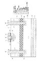
本発明の第1の実施の形態に係る半導体装置のユニットセル部分を示す模式的素子断面構造は、図1に示すように、埋め込み酸化膜3と、埋め込み酸化膜3上に配置された活性層(n-層)4と、活性層4表面近傍に配置されたベース領域5と、ベース領域5内に配置された第1主電極領域7と、活性層4の表面から埋め込み酸化膜3を突き抜けて形成された第2主電極領域8と、ベース領域5に対してゲート絶縁膜12を介して配置されたゲート電極11と、第1主電極領域7に接触する第1主電極9と、第2主電極領域8の内部において第2主電極領域8に接触する第2主電極10と、グラウンド電極1と、p+支持基板21およびp- 層若しくはn-層からなる支持基板22と、支持基板側ドレイン領域13とを備える。
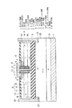
本発明の第2の実施の形態に係る半導体装置のユニットセル部分を示す模式的素子断面構造は、図2に示すように、グラウンド電極1と、グラウンド電極1に接触するp+支持基板21と、p+支持基板21上に配置されたn-層若しくはp-層からなる支持基板22と、支持基板22に接して配置される埋め込み酸化膜3と、埋め込み酸化膜3上に配置され活性層4を構成するnピラー領域14及びpピラー領域15と、pピラー領域15中に配置されるベース領域5と、ベース領域5中に配置されるバックゲート領域6と、同じくベース領域5中に配置されるソース領域7と、活性層4の表面から埋め込み酸化膜3を突き抜けて形成されたドレイン領域8と、バックゲート領域6とソース領域7とに接触するソース電極9と、ドレイン領域8の内部においてドレイン領域8に接触するドレイン電極10と、活性層4の表面から埋め込み酸化膜3内部に至るように、活性層4の表面に対して垂直方向に形成されているゲート電極11と、活性層4の表面から埋め込み酸化膜3に至るように活性層4とゲート電極11との界面に形成されるゲート絶縁膜12と、支持基板側ドレイン領域13と、ソース・ドレイン間において活性層4の表面に配置された絶縁膜18とを備える。
を備える点にある。活性層4と埋め込み酸化膜3との界面に平行な接合面を有するpn接合からなるスーパージャンクション構造を用いてMOSFETのソース・ドレイン間を形成している。
本発明の第3の実施の形態に係る半導体装置のユニットセル部分を示す模式的素子断面構造は、図3に示すように、グラウンド電極1と、グラウンド電極1に接触するp+支持基板21と、p+支持基板21上に配置されたn-層若しくはp-層からなる支持基板22と、支持基板22に接して配置される埋め込み酸化膜3と、埋め込み酸化膜3上に配置され活性層4を構成するpピラー領域16,nピラー領域14及びpピラー領域15と、pピラー領域15中に配置されるベース領域5と、ベース領域5中に配置されるバックゲート領域6と、同じくベース領域5中に配置されるソース領域7と、活性層4の表面から埋め込み酸化膜3を突き抜けて形成されたドレイン領域8と、バックゲート領域6とソース領域7とに接触し、かつ活性層4の表面から埋め込み酸化膜3近傍のpピラー領域16の内部に至るように、活性層4の表面に対して垂直方向に伸延する部分を更に有するソース電極9と、ソース電極9とpピラー領域16内部において接触するpピラーバックゲート用領域17と、ドレイン領域8の内部においてドレイン領域8に接触するドレイン電極10と、活性層4の表面から埋め込み酸化膜3近傍のpピラー領域16の内部に至るように、活性層4の表面に対して垂直方向に形成されているゲート電極11と、活性層4の表面から埋め込み酸化膜3近傍のpピラー領域16の内部に至るように活性層4とゲート電極11との界面に形成されるゲート絶縁膜12と、支持基板側ドレイン領域13と、ソース・ドレイン間において活性層4の表面に配置された絶縁膜18と、を備える。
本発明の第4の実施の形態に係る半導体装置のユニットセル部分を示す模式的素子断面構造は、図4に示すように、グラウンド電極1と、グラウンド電極1に接触するp+支持基板21と、p+支持基板21上に配置されたn-層若しくはp-層からなる支持基板22と、支持基板22に接して配置される埋め込み酸化膜3と、埋め込み酸化膜3上に配置され活性層4を構成するnピラー領域14及びpピラー領域15と、pピラー領域15中に配置されるベース領域5と、ベース領域5中に配置されるバックゲート領域6と、同じくベース領域5中に配置されるソース領域7と、活性層4の表面から埋め込み酸化膜3表面若しくは内部に至るように活性層4の表面に対して垂直方向に形成されたドレイン領域8と、バックゲート領域6とソース領域7とに接触するソース電極9と、ドレイン領域8の内部においてドレイン領域8に接触し、活性層4の表面から埋め込み酸化膜3内部に至るように、活性層4の表面に対して垂直方向に形成されているドレイン電極10と、活性層4の表面から埋め込み酸化膜3内部に至るように、活性層4の表面に対して垂直方向に形成されているゲート電極11と、活性層4の表面から埋め込み酸化膜3に至るように活性層4とゲート電極11との界面に形成されるゲート絶縁膜12と、ソース・ドレイン間において活性層4の表面に配置された絶縁膜18とを備える。
上記のように、本発明は第1乃至第4の実施の形態によって記載したが、この開示の一部をなす論述及び図面はこの発明を限定するものであると理解すべきではない。この開示から当業者には様々な代替実施の形態、実施例及び運用技術が明らかとなろう。
2,21,22…支持基板
3…埋め込み酸化膜(BOX酸化膜)
4…活性層
5…ベース電極
6…バックゲート領域
7…ソース領域
8…ドレイン領域
9…ソース電極
10…ドレイン電極
11…ゲート電極
12…ゲート絶縁膜
13…支持基板側ドレイン領域
14…nピラー領域
15,16…pピラー領域
17…pピラーバックゲート用領域
18…絶縁膜
24…ゲート湾曲部
Claims (5)
- 半導体基板と、
前記半導体基板上に配置された埋め込み絶縁膜と、
前記埋め込み絶縁膜上に配置された活性層と、
前記活性層表面近傍に配置されたベース領域と、
前記ベース領域内に配置された第1主電極領域と、
前記活性層の表面から前記埋め込み絶縁膜の表面まで若しくは突き抜けて形成された第2主電極領域と、
前記ベース領域の表面近傍に配置されたゲート絶縁膜と、
前記ゲート絶縁膜上に配置されたゲート電極と、
前記第1主電極領域に電気的に接触する第1主電極と、
前記第2主電極領域に電気的に接触する第2主電極と、
前記半導体基板の前記埋め込み絶縁膜が配置される面と反対側の面で前記半導体基板に電気的に接触するグラウンド電極
とを備えることを特徴とする半導体装置。 - 前記第2主電極は、前記第2主電極領域の表面から前記埋め込み絶縁膜の内部まで若しくは突き抜けて形成されたことを特徴とする請求項1に記載の半導体装置。
- 前記活性層は、双方が接触する界面でpn接合を形成する第1及び第2ピラー領域を備え、前記第1、第2ピラー領域間のpn接合は、前記活性層が前記埋め込み絶縁膜と接触する面に略平行な接合面を有することを特徴とする請求項1又は2に記載の半導体装置。
- 前記ゲート電極は前記活性層の表面から少なくとも前記埋め込み絶縁膜近傍に至るように、前記活性層の表面に対して垂直方向に形成されていることを特徴とする請求項1乃至請求項3の内、いずれか1項に記載の半導体装置。
- 前記活性層は、各々が接触する界面でpn接合を形成する第1、第2及び第3ピラー領域を備え、前記第1、第2、第3ピラー領域間のpn接合は、前記活性層が前記埋め込み絶縁膜と接触する面に略平行な接合面を有すると共に、前記第1主電極は、前記活性層の表面から前記第1、第2及び第3ピラー領域の内の前記埋め込み絶縁膜側に形成されたピラー領域に至るように、前記活性層の表面に対して垂直方向に伸延する部分を更に有することを特徴とする請求項1,請求項2又は請求項4の内、いずれか1項に記載の半導体装置。
Priority Applications (2)
| Application Number | Priority Date | Filing Date | Title |
|---|---|---|---|
| JP2004107544A JP4334395B2 (ja) | 2004-03-31 | 2004-03-31 | 半導体装置 |
| US11/091,419 US7227226B2 (en) | 2004-03-31 | 2005-03-29 | Semiconductor device with buried-oxide film |
Applications Claiming Priority (1)
| Application Number | Priority Date | Filing Date | Title |
|---|---|---|---|
| JP2004107544A JP4334395B2 (ja) | 2004-03-31 | 2004-03-31 | 半導体装置 |
Publications (2)
| Publication Number | Publication Date |
|---|---|
| JP2005294533A true JP2005294533A (ja) | 2005-10-20 |
| JP4334395B2 JP4334395B2 (ja) | 2009-09-30 |
Family
ID=35308592
Family Applications (1)
| Application Number | Title | Priority Date | Filing Date |
|---|---|---|---|
| JP2004107544A Expired - Fee Related JP4334395B2 (ja) | 2004-03-31 | 2004-03-31 | 半導体装置 |
Country Status (2)
| Country | Link |
|---|---|
| US (1) | US7227226B2 (ja) |
| JP (1) | JP4334395B2 (ja) |
Cited By (3)
| Publication number | Priority date | Publication date | Assignee | Title |
|---|---|---|---|---|
| JP2007158139A (ja) * | 2005-12-07 | 2007-06-21 | Oki Electric Ind Co Ltd | 半導体装置およびその製造方法 |
| JP2015141925A (ja) * | 2014-01-27 | 2015-08-03 | ルネサスエレクトロニクス株式会社 | 半導体装置およびその製造方法 |
| JP2017034154A (ja) * | 2015-08-04 | 2017-02-09 | 株式会社東芝 | 半導体装置 |
Families Citing this family (12)
| Publication number | Priority date | Publication date | Assignee | Title |
|---|---|---|---|---|
| JP2006005275A (ja) * | 2004-06-21 | 2006-01-05 | Toshiba Corp | 電力用半導体素子 |
| US8080851B2 (en) * | 2008-08-29 | 2011-12-20 | International Business Machines Corporation | Deep trench electrostatic discharge (ESD) protect diode for silicon-on-insulator (SOI) devices |
| DE102009018054B4 (de) * | 2009-04-21 | 2018-11-29 | Infineon Technologies Austria Ag | Lateraler HEMT und Verfahren zur Herstellung eines lateralen HEMT |
| KR101154750B1 (ko) * | 2009-09-10 | 2012-06-08 | 엘지이노텍 주식회사 | 발광소자 및 그 제조방법 |
| WO2013073042A1 (ja) * | 2011-11-17 | 2013-05-23 | 富士電機株式会社 | 半導体装置および半導体装置の製造方法 |
| JP6184057B2 (ja) * | 2012-04-18 | 2017-08-23 | ルネサスエレクトロニクス株式会社 | 半導体装置 |
| CN103560145B (zh) * | 2013-11-16 | 2016-08-17 | 重庆大学 | 一种具有界面栅的soi功率器件结构 |
| CN104779282B (zh) * | 2014-01-10 | 2018-01-09 | 帅群微电子股份有限公司 | 沟槽式功率金属氧化物半导体场效晶体管与其制造方法 |
| US20160035899A1 (en) * | 2014-07-30 | 2016-02-04 | Qualcomm Incorporated | Biasing a silicon-on-insulator (soi) substrate to enhance a depletion region |
| US20220384430A1 (en) * | 2018-08-17 | 2022-12-01 | Silergy Semiconductor Technology (Hangzhou) Ltd | Electrode structure, semiconductor structure, and manufacturing method of electrode structure |
| JP7263286B2 (ja) * | 2020-03-24 | 2023-04-24 | 株式会社東芝 | 半導体装置 |
| CN116469908A (zh) * | 2022-08-30 | 2023-07-21 | 苏州华太电子技术股份有限公司 | 半导体器件及其制备方法 |
Family Cites Families (4)
| Publication number | Priority date | Publication date | Assignee | Title |
|---|---|---|---|---|
| US6121661A (en) * | 1996-12-11 | 2000-09-19 | International Business Machines Corporation | Silicon-on-insulator structure for electrostatic discharge protection and improved heat dissipation |
| DE19801095B4 (de) * | 1998-01-14 | 2007-12-13 | Infineon Technologies Ag | Leistungs-MOSFET |
| JP2000332247A (ja) | 1999-03-15 | 2000-11-30 | Toshiba Corp | 半導体装置 |
| FR2826183A1 (fr) * | 2001-06-15 | 2002-12-20 | St Microelectronics Sa | Transistor mos de puissance lateral |
-
2004
- 2004-03-31 JP JP2004107544A patent/JP4334395B2/ja not_active Expired - Fee Related
-
2005
- 2005-03-29 US US11/091,419 patent/US7227226B2/en not_active Expired - Fee Related
Cited By (3)
| Publication number | Priority date | Publication date | Assignee | Title |
|---|---|---|---|---|
| JP2007158139A (ja) * | 2005-12-07 | 2007-06-21 | Oki Electric Ind Co Ltd | 半導体装置およびその製造方法 |
| JP2015141925A (ja) * | 2014-01-27 | 2015-08-03 | ルネサスエレクトロニクス株式会社 | 半導体装置およびその製造方法 |
| JP2017034154A (ja) * | 2015-08-04 | 2017-02-09 | 株式会社東芝 | 半導体装置 |
Also Published As
| Publication number | Publication date |
|---|---|
| US7227226B2 (en) | 2007-06-05 |
| US20050253187A1 (en) | 2005-11-17 |
| JP4334395B2 (ja) | 2009-09-30 |
Similar Documents
| Publication | Publication Date | Title |
|---|---|---|
| US5973341A (en) | Lateral thin-film silicon-on-insulator (SOI) JFET device | |
| JP3837178B2 (ja) | ハイパワーmos型電界効果トレンチトランジスタデバイス | |
| EP2165367B1 (en) | Improved power switching transistors | |
| CN101345243B (zh) | 半导体器件 | |
| CN100576538C (zh) | 双向晶体管及其方法 | |
| JP4334395B2 (ja) | 半導体装置 | |
| US8264015B2 (en) | Semiconductor device wherein a first insulated gate field effect transistor is connected in series with a second field effect transistor | |
| EP2860762B1 (en) | High voltage junction field effect transistor | |
| JP2007013058A (ja) | 半導体装置 | |
| CN102165594A (zh) | 在金属衬底上的半导体异质结构中具有应变沟道的功率mosfet | |
| CN110176454A (zh) | 多晶体管器件 | |
| US10290726B2 (en) | Lateral insulated gate bipolar transistor | |
| US11049942B2 (en) | Power semiconductor device | |
| US20080203535A1 (en) | Semiconductor device | |
| CN114556588B (zh) | 开关元件 | |
| JP5519461B2 (ja) | 横型半導体装置 | |
| JP5720478B2 (ja) | 炭化珪素半導体装置 | |
| TWI447912B (zh) | 半導體裝置及其製造方法 | |
| WO2023037981A1 (ja) | 絶縁ゲート型半導体装置 | |
| JP3376294B2 (ja) | 半導体装置 | |
| JP2018085383A (ja) | スイッチング素子 | |
| JPS60262468A (ja) | Mos型電界効果トランジスタ | |
| CN120583707B (zh) | 具有高k栅介质层和金属栅电极的金属氧化物半导体场效应晶体管 | |
| US12495576B2 (en) | Silicon carbide semiconductor device | |
| CN116153978B (zh) | 一种具有逆导功能的增强型氧化镓功率器件 |
Legal Events
| Date | Code | Title | Description |
|---|---|---|---|
| A977 | Report on retrieval |
Free format text: JAPANESE INTERMEDIATE CODE: A971007 Effective date: 20070219 |
|
| A131 | Notification of reasons for refusal |
Free format text: JAPANESE INTERMEDIATE CODE: A131 Effective date: 20090113 |
|
| A521 | Request for written amendment filed |
Free format text: JAPANESE INTERMEDIATE CODE: A523 Effective date: 20090305 |
|
| A131 | Notification of reasons for refusal |
Free format text: JAPANESE INTERMEDIATE CODE: A131 Effective date: 20090424 |
|
| A521 | Request for written amendment filed |
Free format text: JAPANESE INTERMEDIATE CODE: A523 Effective date: 20090513 |
|
| TRDD | Decision of grant or rejection written | ||
| A01 | Written decision to grant a patent or to grant a registration (utility model) |
Free format text: JAPANESE INTERMEDIATE CODE: A01 Effective date: 20090602 |
|
| A01 | Written decision to grant a patent or to grant a registration (utility model) |
Free format text: JAPANESE INTERMEDIATE CODE: A01 |
|
| A61 | First payment of annual fees (during grant procedure) |
Free format text: JAPANESE INTERMEDIATE CODE: A61 Effective date: 20090623 |
|
| FPAY | Renewal fee payment (event date is renewal date of database) |
Free format text: PAYMENT UNTIL: 20120703 Year of fee payment: 3 |
|
| FPAY | Renewal fee payment (event date is renewal date of database) |
Free format text: PAYMENT UNTIL: 20120703 Year of fee payment: 3 |
|
| FPAY | Renewal fee payment (event date is renewal date of database) |
Free format text: PAYMENT UNTIL: 20130703 Year of fee payment: 4 |
|
| LAPS | Cancellation because of no payment of annual fees |