JP2005294633A - Semiconductor light emitting device - Google Patents
Semiconductor light emitting device Download PDFInfo
- Publication number
- JP2005294633A JP2005294633A JP2004109159A JP2004109159A JP2005294633A JP 2005294633 A JP2005294633 A JP 2005294633A JP 2004109159 A JP2004109159 A JP 2004109159A JP 2004109159 A JP2004109159 A JP 2004109159A JP 2005294633 A JP2005294633 A JP 2005294633A
- Authority
- JP
- Japan
- Prior art keywords
- layer
- pulsation
- laser
- light
- type
- Prior art date
- Legal status (The legal status is an assumption and is not a legal conclusion. Google has not performed a legal analysis and makes no representation as to the accuracy of the status listed.)
- Pending
Links
Images


Landscapes
- Semiconductor Lasers (AREA)
Abstract
【課題】 パルセーションレーザにおけるパルセーションの安定化を図り、温度、パワーバンドに対するマージンを拡大してパルセーションレーザの使用できる範囲の拡大を図る。
【解決手段】 活性層25と、該活性層25を挟む下側クラッド層24及び上側クラッド層26とを有するパルセーションレーザの、少なくとも下側クラッド層24に該下側クラッド層24より屈折率が大きく光の分布をコントロールする光コントロール層32が設けられて成る。
【選択図】 図1
PROBLEM TO BE SOLVED: To stabilize a pulsation in a pulsation laser and expand a margin for a temperature and a power band to expand a usable range of the pulsation laser.
A pulsation laser having an active layer and a lower clad layer and an upper clad layer sandwiching the active layer has a refractive index higher than that of the lower clad layer at least in the lower clad layer. A light control layer 32 that largely controls the light distribution is provided.
[Selection] Figure 1
Description
本発明は、パルセーションレーザを主体とした半導体レーザ、マルチレーザ、あるいは光集積回路等の、いわゆる半導体発光装置に関する。 The present invention relates to a so-called semiconductor light emitting device such as a semiconductor laser mainly composed of a pulsation laser, a multilaser, or an optical integrated circuit.
光ディスク用の半導体レーザとして、例えば情報の読み取りの用途において、半導体レーザへの戻り光により発生するノイズを抑制可能にしたパルセーション(自励発振)動作する半導体レーザ(パルセーションレーザ)が提案されている(特許文献1、2参照)。このパルセーションレーザには、活性層の近くに過飽和吸収層(SAL;Saturable Absorbing layer)を設けたSAL型と、インディクスガイドとゲインガイドの中間的な導波ガイドを実現する弱い屈折率差を設定し、動作時に活性層内部に過飽和吸収領域が形成されるWI(Weakly Index guide)型とがある。
As a semiconductor laser for an optical disk, for example, a semiconductor laser (pulsation laser) that operates in a pulsation (self-pulsation) mode capable of suppressing noise generated by light returned to the semiconductor laser in an information reading application has been proposed. (See
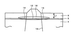
図5は、従来のWI型のパルセーションレーザの概略的構成を示す。このパルセーションレーザ1は、例えばn型基板2上にn型バッファ層3、n型クラッド層4、活性層5、p型クラッド層6、n型中間層7及びn型コンタクト層8が積層され、n型コンタクト層8、n型中間層7及びp型クラッド層6の一部にわたってメサエッチングされ、メサエッチングの両側にn型電流ブロック層9が形成されて成る。基板1の裏面にはn電極10が形成され、コンタクト層8上にはp電極11が形成される。
このパルセーションレーザ1では、図6に示すように、動作時に活性層3内のレーザ発振領域13の両側に過飽和吸収領域14が形成され、パルセーション動作が行われる。レーザ発振領域13は光の分布16と電流分布15とが重なる領域に形成され、過飽和吸収領域14は活性層5の光の分布16と重なる領域に形成される。このようなパルセーションレーザ1においては、通常図6に示すように、光の分布16がp型クラッド層6側に寄って形成されている。
In the
パルセーションレーザにおいては、パルセーション動作がレーザ素子の温度、パワーバンド(レーザ出力パワー)に依存しており、パルセーションを安定させて使用できる範囲、即ちその使用される温度、パワーバンドの範囲が制限される。従来のパルセーション構造では、高温、高パワー、あるいは低温、低パワーになると、パルセーションが不安定になり、使用できる範囲が限定されていた。例えば、温度上昇すると温度に応じてキャリアが発生し、このキャリアも過飽和吸収領域に吸収され過飽和吸収領域の光吸収容量が減る。また、高パワーにすることは電流を多く流すことになり、それにつれて電流の広がりも大きくなり、過飽和吸収領域の体積が減る。つまり、光の吸収能力が落ちることで、使用範囲が限られる。
従って、パルセーションの温度、パワーバンドに対するマージンを高め、パルセーションレーザとして使用できる範囲の拡大が望まれていた。
In the pulsation laser, the pulsation operation depends on the temperature and power band (laser output power) of the laser element, and the range in which the pulsation can be stably used, that is, the temperature and power band range to be used is Limited. In the conventional pulsation structure, the pulsation becomes unstable at high temperature, high power, low temperature and low power, and the usable range is limited. For example, when the temperature rises, carriers are generated according to the temperature, and the carriers are also absorbed in the supersaturated absorption region, and the light absorption capacity of the supersaturated absorption region is reduced. Further, when the power is increased, a large amount of current flows, and the spread of the current increases accordingly, and the volume of the supersaturated absorption region decreases. That is, the range of use is limited due to a decrease in light absorption capability.
Therefore, it has been desired to increase the margin for the temperature and power band of the pulsation and expand the range that can be used as a pulsation laser.
本発明は、上述の点に鑑み、パルセーションを安定化させ、温度、パワーバンドに対するマージンを高めて使用できる範囲を広げるようにした半導体発光装置を提供するものである。 In view of the above, the present invention provides a semiconductor light-emitting device that stabilizes pulsation and increases the margin for temperature and power band to widen the usable range.
本発明に係る半導体発光装置は、活性層と、この活性層を挟む下側クラッド層及び上側クラッド層とを有するパルセーションレーザの、少なくとも下側クラッド層にこの下側クラッド層より屈折率が大きく光の分布をコントロールする光コントロール層を設けて構成する。 The semiconductor light emitting device according to the present invention has a refractive index larger than that of the lower cladding layer in at least the lower cladding layer of a pulsation laser having an active layer and a lower cladding layer and an upper cladding layer sandwiching the active layer. A light control layer for controlling the light distribution is provided.
本発明は、上記半導体発光装置において、光コントロール層により光の分布をより活性層に近づくようにコントロールして、活性層内に過飽和吸収領域を形成するように構成する。
本発明は、上記半導体発光装置において、さらに上側クラッド層にこの上側クラッド層より屈折率が大きく光の分布をコントロールする光コントロール層を設けて構成する。
According to the present invention, in the semiconductor light emitting device, a light distribution is controlled by the light control layer so as to be closer to the active layer, and a supersaturated absorption region is formed in the active layer.
In the semiconductor light emitting device according to the present invention, a light control layer having a higher refractive index than that of the upper cladding layer and controlling the light distribution is further provided in the upper cladding layer.
本発明の半導体発光装置では、パルセーションレーザの少なくとも下側クラッド層、例えば下側クラッド層に、もしくは上側クラッド層と下側クラッド層の両方に、これより屈折率が大きい光コントロール層が設けられることにより、動作時の光の分布が下側クラッド層側に引きつけられ、活性層に近づくようになる。光の分布が活性層に近づくことで、レーザ発振領域を挟む両側に形成される光の分布と活性層が重なる過飽和吸収領域が広がる。 In the semiconductor light emitting device of the present invention, a light control layer having a higher refractive index is provided on at least the lower cladding layer of the pulsation laser, for example, the lower cladding layer, or both the upper cladding layer and the lower cladding layer. As a result, the light distribution during operation is attracted to the lower clad layer side and approaches the active layer. As the light distribution approaches the active layer, the supersaturated absorption region where the active layer overlaps with the light distribution formed on both sides of the laser oscillation region is expanded.
本発明に係る半導体発光装置によれば、パルセーションレーザにおける電流分布を変えずに過飽和吸収領域が広がるので、パルセーションが安定化する。これにより、温度、パワーバンドに対するマージンを拡大することができ、パルセーションレーザの使用できる範囲を広げることができる。また、パルセーションレーザの設計の自由度を拡大することができる。 According to the semiconductor light emitting device of the present invention, the supersaturated absorption region is expanded without changing the current distribution in the pulsation laser, so that the pulsation is stabilized. Thereby, the margin with respect to temperature and a power band can be expanded, and the range which can use a pulsation laser can be expanded. In addition, the degree of freedom in designing the pulsation laser can be expanded.
以下、図面を参照して本発明の実施の形態を説明する。 Embodiments of the present invention will be described below with reference to the drawings.
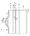
図1は、本発明に係る半導体発光装置をパルセーションレーザに適用した実施の形態を示す。本実施の形態に係るパルセーションレーザ21は、第1導電型の半導体基体22上に第1導電型のバッファ層23、第1導電型のクラッド層24、活性層25、第2導電型のクラッド層26、第2導電型の中間層27及び第2導電型のコンタクト層28が積層され、第2導電型のコンタクト層28、中間層27及びクラッド層26の一部にわたってメサエッチングされ、そのメサ部の両側面及びメサ部より連続する第2導電型のクラッド層26の上面にわたって第1導電型の電流ブロック層29が形成される。基体22の裏面には、第1導電側電極30が形成され、コンタク層28の上面、本例では電流ブロク層29の上面に延長するように第2導電側電極31が形成される。
FIG. 1 shows an embodiment in which a semiconductor light emitting device according to the present invention is applied to a pulsation laser. The
そして、本実施の形態においては、特に第1導電型のクラッド層24内に、動作時に形成される光の分布をコントロールする光コントロール層32が形成される。この光コントロール層32は第1導電型のクラッド層24の屈折率より大きい屈折率の層で形成され、且つ光を吸収しない層で形成される。光コントロール層32は、レーザ21の共振器長方向の全長、及びこれと直交する全幅にわたって形成することができる。また、光コントロール層32と活性層25間の距離d1及び光コントロール層32の層厚t1は光の分布を光コントロール層32側へ寄せるコントロール量により設定することができる。
In the present embodiment, the
本例では、基体22として、nーGaAs基板を用い、このn型基板22上に、nーGaAs層(基板側)とnーGaInP層(クラッド層側)とによるn型バッファ層23、nー(Al0.7Ga0.3)0.5In0.5P層(厚さ1.1μm)のn型クラッド層24、Ga0.5In0.5 P層のn型光コントロール層32、n-(Al0.7Ga0.3)0.5In0.5P層(厚さ0.4μm)のn型クラッド層24、ノンドープGa0.5 In0.5 P層の活性層25、p−(Al0.7Ga0.3)0.5In0.5P層(厚さ0.4μm)のP型クラッド層26、pーGa0.5In0.5 P層のp型中間層27、pーGaAs層のp型コンタクト層28、nーGaAs層の電流ブロック層29が形成され、n型基板22の裏面に下から順次AuGe/Ni/Auを積層したn電極30がオーミック接続され、p型コンタクト層28に下から順次Ti/Pt/Auを積層したp電極31がオーミック接続される。光コントロール層32としては、n型クラッド層24より高屈折率とするため、AlGaInP系において、そのAl量をn型クラッド層24のAl量より少なくした(0を含む)組成とすることができる。
In this example, an n-GaAs substrate is used as the
なお、活性層に多重量子井戸構造(MQW)、例えばAlGaInP層とGaInP層を繰り返し積層してなるMQWを用いた構成とすることもできる。また、活性層とクラッド層との間にガイド層を有する構成とすることもできる。
パルセーションレーザ21の各層は、上例の組成に限らず目的に応じて例えばレーザ波長等により種々の組成で形成することができる。
The active layer may have a multiple quantum well structure (MQW), for example, an MQW formed by repeatedly laminating an AlGaInP layer and a GaInP layer. Moreover, it can also be set as the structure which has a guide layer between an active layer and a clad layer.
Each layer of the
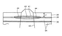
本実施の形態のパルセーションレーザ21では、動作時に図2に示すように、活性層25内の光の分布41と電流分布42とが重なる領域にレーザ発振領域43が形成され、このレーザ発振領域43の両側に過飽和吸収領域44が形成され、パルセーション動作が行われる。このとき、n型クラッド層24内に設けられた光コントロール層32により、光の分布41は、鎖線で示す従来の光の分布16より活性層25側に寄せられる。即ち、模式的にみると、従来の場合は扁平な楕円状の光の分布16が層の構成により活性層から外れる形になる場合がある。しかし、本実施の形態では、光コントロール層32により光の分布41が活性層25の中心に近づき、光分布41に両先端部41aが活性層25内に存するようになる。このため、光の分布41と活性層25とが重なる過飽和吸収領域44が広がる。この過飽和吸収領域44が広くなることで、光の吸収能力が向上し、パルセーションが安定化し、使用範囲の拡大が図れる。
In the
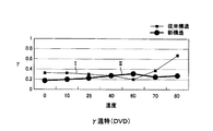
このように光コントロール層32によって光の分布41がより活性層25の中心に近づくことで、電流分布42と光の分布41との差、すなわちキャリアが注入されている領域(電流分布)と、電流注入が不十分で光のゲインが取れていない領域(光の分布)の差が大きくなり、パルセーションを強くすることができる。図3は、パルセーションの強弱を示すパラメータとしてγを使用したときのγ温度特性を示す。なお、このγ温度特性は、デジタルビデオディスク(DVD)での測定である。γは可干渉性といい、レーザの干渉の度合いを示し、次のように定義されます。λ指定光出力1で測定したときの波長データの最大レベルを1とした時のセカンドピークをγとする。γ値が大きいと干渉が強いことを意味し、パルセーション(自励発振)が弱くなる。
Thus, the
図3において、曲線Iは光コントロール層を有しない従来構造のパルセーションレーザであり、曲線IIは光コントロール層を挿入した本発明構造のパルセーションレーザである。γ値としては、0.5以下が望ましいと考えられる。図3によれば、従来構造のパルセーションレーザ1では、80℃(高温)でγ値が0.5を大きく越えているのに対し、本発明構造のパルセーションレーザ21は80℃(高温)でγ値が0.5以下に抑えられている。
In FIG. 3, curve I is a pulsation laser having a conventional structure without a light control layer, and curve II is a pulsation laser having a structure of the present invention in which a light control layer is inserted. As the γ value, 0.5 or less is considered desirable. According to FIG. 3, in the
本実施の形態に係るパルセーションレーザ21によれば、パルセーションを安定化することができ、温度、パワーバンド(いわゆるレーザの出射パワーの範囲)に対するマージンを拡大することができる。従って、パルセーションレーザとしての使用できる範囲を広げることができる。また、温度、パワーバンドに対するマージンを拡大できるので、パルセーションレーザの設計の自由度を拡大することができる。
According to the
因みに、図5の従来構造において、活性層と電流ブロック層間の距離を大きくすれば、光の閉じ込めが弱くなり光の分布が広がり過飽和吸収領域を広げることができるが、同時に電流分布も広がるために、動作電流を上げることになり、発熱して結果的にパルセーションが悪くなる。本実施の形態では、活性層25と電流ブロック層29間の距離L1を変えずに電流分布42の広がりを抑え、また、光の分布を広げ過ぎることなく、光コントロール層32によって光の分布41をより活性層25側に引き付けて過飽和吸収領域を広げことができるので、特性を変化させずにパルセーションを強くすることができる。
Incidentally, in the conventional structure of FIG. 5, if the distance between the active layer and the current block layer is increased, the light confinement is weakened and the light distribution is widened to expand the supersaturated absorption region. As a result, the operating current is increased and heat is generated, resulting in poor pulsation. In the present embodiment, the
一方、活性層とクラッド層の間に光ガイド層を有するパルセーションレーザに適用した場合には、光ガイド層、p型クラッド層の厚さ、活性層体積を微調整することで、静特性を変化させることなく、パルセーションを強くすることができる。 On the other hand, when applied to a pulsation laser having a light guide layer between the active layer and the clad layer, the static characteristics can be improved by finely adjusting the thickness of the light guide layer, the p-type clad layer, and the volume of the active layer. The pulsation can be strengthened without changing it.
上述の図1における実施の形態に係るパルセーションレーザ21は、光コントロール層32をn型クラッド層24に設けた構成としたが、さらにpクラッド層26側にも光コントロール層を設ける構成とすることができる。
The
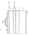
図4は、n型クラッド層24とp型クラッド層26に光コントロール層36を設けた本発明に係るパルセーションレーザの他の実施の形態を示す。
本実施の形態に係るパルセーションレーザ35は、前述と同様に基体22上に、バッファ層23、第1導電型の例えばn型クラッド層24、活性層25、第2導電型の例えばp型クラッド層26、中間層27、コンタクト層28、電流ブロック層29、両電極30、31を有する。そして、n型クラッド層24内に第1の光コントロール層32を形成するとともに、p型クラッド層26内に第2の光コントロール層36を形成して構成される。この第2の光コントロール層36は、エッチングストップ層として利用することもできる。各層を例えば前述と同様の組成で形成したときには、第2の光コントロール層36は、Ga0.5In0.5 P層で形成することができる。第2の光コントロール層36は、p型クラッド層26より大きい屈折率の層で形成されかつ光を吸収しない層で形成され、例えば第1の光コントロール層32と導電型を異にして同じ組成で形成することができる。
FIG. 4 shows another embodiment of the pulsation laser according to the present invention in which the light control layer 36 is provided on the n-
The
すなわち、本例では、nーGaAs基板22上に、nーGaAs層(基板側)とnーGaInP層(クラッド層側)とによるn型バッファ層23、nー(Al0.7Ga0.3)0.5In0.5P層のn型クラッド層24、Ga0.5In0.5 P層のn型光コントロール層32、nー(Al0.7Ga0.3)0.5In0.5P層のn型クラッド層24、ノンドープGa0.5 In0.5 P層の活性層25、p−(Al0.7Ga0.3)0.5In0.5P層のP型クラッド層26、Ga0.5In0.5P層のp型光コントロール層36、p−(Al0.7Ga0.3)0.5In0.5P層のP型クラッド層26、pーGa0.5In0.5 P層のp型中間層27、pーGaAs層のp型コンタクト層28、nーGaAs層の電流ブロック層29が形成され、n型基板22の裏面に下から順次AuGe/Ni/Auを積層したn電極30がオーミック接続され、p型コンタクト層28に下から順次Ti/Pt/Auを積層したp電極31がオーミック接続される。
That is, in this example, on the n-
本実施の形態に係るパルセーションレーザ35によれば、n型クラッド層24内に設けられた第1の光コントロール層32とp型クラッド層26内に設けられた第2の光コントロール層36により光の分布がコントロールされ、図2と同様に光の分布41をより活性層25側に寄せて過飽和吸収領域を拡大することができる。従って、この構成においても、パルセーションを安定化することができ、温度、パワーバンドに対するマージンを拡大することができる。従って、パルセーションレーザとしての使用できる範囲を広げることができる。また、温度、パワーバンドに対するマージンを拡大できるので、パルセーションレーザの設計の自由度を拡大することができる。
According to the
図5は、本発明に係るパルセーションレーザのさらに他の実施の形態を示す。本例は、n型クラッド層24とp型クラッド層26に光コントロール層36を設けた場合であるが、図4と構成を異にする。本実施の形態に係るパルセーションレーザ37は、前述の図4と同様に基体22上に、バッファ層23、第1導電型の例えばn型クラッド層24、活性層25、第2導電型の例えばp型クラッド層26、中間層27、コンタクト層28、電流ブロック層29、両電極30、31を有する。そして、n型クラッド層24内に第1の光コントロール層32を形成するとともに、p型クラッド層26内に第2の光コントロール層36を形成して構成される。
FIG. 5 shows still another embodiment of the pulsation laser according to the present invention. In this example, the light control layer 36 is provided in the n-
本実施の形態では、特に、第2の光コントロール層36とその上のp型クラッド層26、中間層27、コンタクト層28が電流ブロック層29により幅が規制された構造に形成される。各層の組成は、例えば図4と同様の組成で形成することができる。
In the present embodiment, in particular, the second light control layer 36 and the p-
本実施の形態にかかるパルセーションレーザ37によれば、図4のパルセーションレーザ35と同様に、n型クラッド層24内に設けられた第1の光コントロール層32とp型クラッド層26内に設けられた第2の光コントロール層36により光の分布がコントロールされ、図2と同様に光の分布41をより活性層25側に寄せて過飽和吸収領域を拡大することができる。従って、この構成においても、パルセーションを安定化することができ、温度、パワーバンドに対するマージンを拡大することができる。従って、パルセーションレーザとしての使用できる範囲を広げることができる。また、温度、パワーバンドに対するマージンを拡大できるので、パルセーションレーザの設計の自由度を拡大することができる。
According to the pulsation laser 37 according to the present embodiment, in the first
本発明のパルセーションレーザとしては、上例の他、活性層とクラッド層の間に光ガイド層を設けた構成のレーザにも適用できる。 The pulsation laser of the present invention can be applied to a laser having a configuration in which a light guide layer is provided between the active layer and the clad layer in addition to the above example.
上述の実施の形態では、本発明をパルセーションレーザ素子に適用した場合であるが、その他、パルセーションレーザを主体としたマルチレーザ、あるいはパルセーションレーザを組み込んだ例えばレーザカプラ等の光集積回路等にも適用することができる。 In the above-described embodiment, the present invention is applied to a pulsation laser element. In addition, a multi-laser mainly including a pulsation laser, or an optical integrated circuit such as a laser coupler incorporating a pulsation laser, etc. It can also be applied to.
21、35、37・・パルセーションレーザ、22・・基体、23・・バッファ層、24・・n型クラッド層、25・・活性層、26・・p型クラッド層、27・・中間層、28・・コンタクト層、29・・電極ブロック層、30、31・・電極、32、36・・光コントロール層、41・・光の分布、42・・電極分布、43・・レーザ発振領域、44・・過飽和吸収領域 21, 35, 37 ..Pulsation laser, 22 ..Substrate, 23 ..Buffer layer, 24 ..n-type cladding layer, 25 ..active layer, 26 ..p-type cladding layer, 27. 28..Contact layer, 29..Electrode block layer, 30, 31..Electrode, 32, 36..Light control layer, 41..Light distribution, 42..Electrode distribution, 43..Laser oscillation region, 44. ..Supersaturated absorption region
Claims (3)
少なくとも前記下側クラッド層に該下側クラッド層より屈折率が大きく光の分布をコントロールする光コントロール層が設けられて成る
ことを特徴とする半導体発光装置。 A pulsation laser having an active layer, and a lower clad layer and an upper clad layer sandwiching the active layer,
A semiconductor light emitting device characterized in that at least the lower clad layer is provided with a light control layer having a refractive index larger than that of the lower clad layer and controlling the light distribution.
ことを特徴とする請求項1記載の半導体発光装置。 2. The semiconductor light emitting device according to claim 1, wherein a light distribution is controlled by the light control layer so as to be closer to the active layer, and a saturable absorption region is formed in the active layer.
ことを特徴とする請求項1記載の半導体発光装置。
2. The semiconductor light emitting device according to claim 1, wherein a light control layer having a refractive index larger than that of the upper cladding layer and controlling the light distribution is provided on the upper cladding layer.
Priority Applications (1)
| Application Number | Priority Date | Filing Date | Title |
|---|---|---|---|
| JP2004109159A JP2005294633A (en) | 2004-04-01 | 2004-04-01 | Semiconductor light emitting device |
Applications Claiming Priority (1)
| Application Number | Priority Date | Filing Date | Title |
|---|---|---|---|
| JP2004109159A JP2005294633A (en) | 2004-04-01 | 2004-04-01 | Semiconductor light emitting device |
Publications (1)
| Publication Number | Publication Date |
|---|---|
| JP2005294633A true JP2005294633A (en) | 2005-10-20 |
Family
ID=35327208
Family Applications (1)
| Application Number | Title | Priority Date | Filing Date |
|---|---|---|---|
| JP2004109159A Pending JP2005294633A (en) | 2004-04-01 | 2004-04-01 | Semiconductor light emitting device |
Country Status (1)
| Country | Link |
|---|---|
| JP (1) | JP2005294633A (en) |
Citations (1)
| Publication number | Priority date | Publication date | Assignee | Title |
|---|---|---|---|---|
| JPS63202083A (en) * | 1987-02-18 | 1988-08-22 | Hitachi Ltd | semiconductor laser equipment |
-
2004
- 2004-04-01 JP JP2004109159A patent/JP2005294633A/en active Pending
Patent Citations (1)
| Publication number | Priority date | Publication date | Assignee | Title |
|---|---|---|---|---|
| JPS63202083A (en) * | 1987-02-18 | 1988-08-22 | Hitachi Ltd | semiconductor laser equipment |
Similar Documents
| Publication | Publication Date | Title |
|---|---|---|
| JP4805887B2 (en) | Semiconductor laser device | |
| JP4657337B2 (en) | Semiconductor laser device | |
| CN109417276B (en) | Semiconductor laser device, semiconductor laser module, and laser light source system for welding | |
| EP1515405A2 (en) | Semiconductor laser | |
| JP4750238B2 (en) | Semiconductor light emitting device | |
| US7704759B2 (en) | Semiconductor laser device and method for fabricating the same | |
| JP4126873B2 (en) | Semiconductor laser device | |
| US20150340840A1 (en) | Semiconductor laser | |
| US7095769B2 (en) | Semiconductor laser diode with higher-order mode absorption layers | |
| JPH1098233A (en) | Semiconductor laser and its manufacturing method | |
| US7092422B2 (en) | Self-pulsation type semiconductor laser | |
| US6333946B1 (en) | Semiconductor laser device and process for manufacturing the same | |
| JP3792434B2 (en) | Self-oscillation type semiconductor laser | |
| JP4661061B2 (en) | Pulsation laser element | |
| JP4544665B2 (en) | Semiconductor laser | |
| JP2005268754A (en) | Semiconductor laser device, method for manufacturing semiconductor laser device, optical disk device, and optical transmission system | |
| JP2002223038A (en) | Semiconductor laser device | |
| JP2005317954A (en) | Semiconductor light emitting device | |
| JP2010192769A (en) | Semiconductor laser device and method of manufacturing the same | |
| JP2000091699A (en) | Semiconductor laser device | |
| JP2006269921A (en) | Semiconductor laser device | |
| JP2005150301A (en) | Semiconductor laser device | |
| JP2005236147A (en) | Semiconductor laser element | |
| JP2003023213A (en) | Semiconductor laser | |
| JP2001274509A (en) | Semiconductor laser |
Legal Events
| Date | Code | Title | Description |
|---|---|---|---|
| A621 | Written request for application examination |
Effective date: 20070323 Free format text: JAPANESE INTERMEDIATE CODE: A621 |
|
| A977 | Report on retrieval |
Effective date: 20091208 Free format text: JAPANESE INTERMEDIATE CODE: A971007 |
|
| A131 | Notification of reasons for refusal |
Free format text: JAPANESE INTERMEDIATE CODE: A131 Effective date: 20100105 |
|
| A521 | Written amendment |
Effective date: 20100224 Free format text: JAPANESE INTERMEDIATE CODE: A523 |
|
| A02 | Decision of refusal |
Effective date: 20101207 Free format text: JAPANESE INTERMEDIATE CODE: A02 |