JP2005294639A - Flex rigid wiring board - Google Patents
Flex rigid wiring board Download PDFInfo
- Publication number
- JP2005294639A JP2005294639A JP2004109237A JP2004109237A JP2005294639A JP 2005294639 A JP2005294639 A JP 2005294639A JP 2004109237 A JP2004109237 A JP 2004109237A JP 2004109237 A JP2004109237 A JP 2004109237A JP 2005294639 A JP2005294639 A JP 2005294639A
- Authority
- JP
- Japan
- Prior art keywords
- flex
- pattern
- wiring board
- rigid
- thickness
- Prior art date
- Legal status (The legal status is an assumption and is not a legal conclusion. Google has not performed a legal analysis and makes no representation as to the accuracy of the status listed.)
- Granted
Links
Images



Landscapes
- Structure Of Printed Boards (AREA)
- Combinations Of Printed Boards (AREA)
Abstract
Description
本発明は、折り曲げ可能な可撓性を有するフレックス部と硬質材料からなるリジッド部とからなるフレックスリジッドプリント配線板に関する。 The present invention relates to a flex-rigid printed wiring board composed of a flex portion having flexibility and a rigid portion made of a hard material.
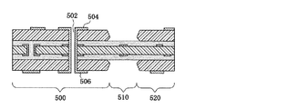
近年、折りたたみ式の携帯電話等の携帯用電子機器には、フレックスリジッド多層配線板が使用されている。このような配線板は、図11に示すように柔軟性がないリジッド部500、520と、柔軟性のあるフレキシブル部510とをフレキシブル基板544を介して連結するとともに、リジッド部500においては、積層するフレキシブル基板544およびリジッド基板500、520表面のパターン層504、506を、めっきスルーホール502の導体層を介して電気的に接続するものが一般的である(例えば、特許文献1参照)。
上記従来技術にかかるフレックスリジッド多層配線板は、ガラスエポキシ樹脂や、ガラスポリイミド樹脂等の硬質基材上に回路形成されてなるリジッド基板の間に、ポリイミド樹脂フィルムやポリエステル樹脂フィルム等の屈曲性能に優れた基材上に回路形成されてなるフレキシブル基板をプリプレグあるいは接着シート等を介して熱圧着し、その後、穴あけ、スルーホールメッキ、レジスト塗布、エッチングといった多くの工程を経て製造されている。 The above-mentioned flex-rigid multilayer wiring board according to the prior art has a bending performance such as a polyimide resin film or a polyester resin film between rigid substrates formed on a hard substrate such as a glass epoxy resin or a glass polyimide resin. A flexible substrate having a circuit formed on an excellent substrate is thermocompression-bonded via a prepreg or an adhesive sheet, and then manufactured through many processes such as drilling, through-hole plating, resist coating, and etching.
上記フレキシブル基板は、自由に折り曲げられることが要求されるため、リジット基板で使用されているような紙や、ガラス繊維等の強化材は使用されず、絶縁材として屈曲性に優れた薄いポリイミド樹脂やポリエステル樹脂などのベースフィルムが採用され、そのベースフィルムに対して柔軟な銅箔を貼り合せたものが基板材料として使用されている。 Since the flexible substrate is required to be bent freely, paper or a reinforcing material such as glass fiber used in a rigid substrate is not used, and a thin polyimide resin having excellent flexibility as an insulating material A base film such as polyester resin or the like is employed, and a flexible copper foil bonded to the base film is used as a substrate material.
このベースフィルムとして用いられるポリイミドフィルムは、フィルム単体では400℃以上の耐熱性があり、部品実装時の250℃以上の半田付け温度にも十分耐える上、実際に機器組み込み後の環境変化に対しても安定した性能が発揮できるため、ポリエステルフィルムよりも圧倒的に多く使用されている。 The polyimide film used as the base film has a heat resistance of 400 ° C or higher when used alone, and can withstand the soldering temperature of 250 ° C or higher when mounting components. Since it can exhibit stable performance, it is overwhelmingly used more than polyester film.
また、ベースフィルム上に貼付された柔軟な銅箔をエッチングして形成される導体回路を保護するためのカバーレイは、屈曲性を考慮して、接着剤付きのポリイミドフィルムが使用されることが多い。 In addition, as a coverlay for protecting a conductor circuit formed by etching a flexible copper foil affixed on a base film, a polyimide film with an adhesive may be used in consideration of flexibility. Many.
ところで、携帯用電子機器の高機能化および高密度化という社会的要請に応じて、実装部品のより一層の小型化が図られると共に、それに伴なって、実装される基板の配線幅の一層の微細化が求められているのが現状である。
とくに、折り曲げ可能なフレックスリジッド配線板においても、それを構成するフレキシブル基板に形成される配線パターンの微細化および高密度化(単位面積辺りの配線の本数を増やす)が求められている。
By the way, in response to the social demand for higher functionality and higher density of portable electronic devices, the mounting components are further reduced in size, and accordingly, the wiring width of the substrate to be mounted is further increased. At present, miniaturization is required.
In particular, a flex-rigid wiring board that can be bent is also required to have a finer and higher-density wiring pattern (increase the number of wirings per unit area) formed on a flexible substrate constituting the flexible rigid wiring board.
しかしながら、フレキシブル基板の絶縁性基材として用いられているポリイミドフィルムは、吸水性が高く、しかも寸法変化が大きいため、ランド径のサイズを予め大きく形成しなければならない等の設計デザイン的な制約を受け、更に、合せ精度を向上させるためにワークサーズを小さくして製造する必要があった。そのため、優れた接続信頼性を得ることができないという問題があり、また、ヒートサイクル等の信頼性試験においても同様の問題があった。 However, the polyimide film used as the insulating base material of the flexible substrate has high water absorption and large dimensional change. Therefore, there are restrictions on design and design such as the land size must be formed in advance. In addition, in order to improve the alignment accuracy, it was necessary to manufacture with a smaller work size. For this reason, there is a problem that excellent connection reliability cannot be obtained, and there is a similar problem in reliability tests such as heat cycle.
また、フレキシブル基板の絶縁性基材として用いられるポリイミド等の樹脂フィルムは、フィルム単体で形成されたもので、芯材に樹脂含浸させたものではないため、(1)十分な強度を確保できない、(2)屈曲部の曲率を一定に保持できない、(3)前記(1)、(2)の故に、屈曲部付近でフレキシブル基材が変形したり、導体回路が断線したりするという問題があった。特に、フレキシブル基材の折り曲げを繰り返したり、導体回路が微細な配線パターンにより形成されているとき場合には、それらの問題が顕著となる。 In addition, a resin film such as polyimide used as an insulating base material of a flexible substrate is formed of a single film, and is not impregnated with a resin in a core material. (1) It cannot ensure sufficient strength. (2) The curvature of the bent portion cannot be kept constant. (3) Because of the above (1) and (2), there is a problem that the flexible base material is deformed near the bent portion or the conductor circuit is disconnected. It was. In particular, when the bending of the flexible base material is repeated or the conductor circuit is formed by a fine wiring pattern, those problems become significant.
また、フレキシブル基板の屈曲部分や、リジット部形成領域付近でウネリ(波状)が形成されることがあり、このウネリが形成されると、基材のうねり形成部分に亀裂が生じたり、導体回路が断線するというダメージを受けることがある。 In addition, undulation (wave shape) may be formed near the bent portion of the flexible substrate or the rigid portion formation region. When this undulation is formed, the undulation formation portion of the base material is cracked or the conductor circuit is Damage may occur due to disconnection.
さらに、フレキシブル基板に設けた導体回路を保護するためのカバーレイを、接着剤付きポリイミドフィルムから形成する場合に、スルーホールの接続信頼性や絶縁信頼性が低下するおそれがあるので、穴明け、デスミア、めっき条件等を特別に管理する必要があると共に、他の材料との組み合わせ構成をする上で制約を受けるという問題もあった。 Furthermore, when forming a coverlay for protecting the conductor circuit provided on the flexible substrate from a polyimide film with an adhesive, the connection reliability and insulation reliability of the through hole may be reduced. In addition to special management of desmear, plating conditions, etc., there is also a problem that there are restrictions on the combination configuration with other materials.
そこで、本発明の目的は、従来技術が抱える上述した問題を解消し、屈曲部での強度を十分に確保しつつ、そこでの屈曲具合を大きく、かつ一定に保持できるようなフレックスリジット配線板を提案することにある。
本発明の他の目的は、フレキシブル基板の屈曲部付近で生じやすい基材の変形や、導体回路の断線、ウネリ形成等を防止できる接続信頼性に優れるフレックスリジット配線板を提案することにある。
Accordingly, an object of the present invention is to provide a flex-rigid wiring board that can solve the above-mentioned problems of the prior art, and can secure a sufficient strength at the bent portion while maintaining a large and constant bending state. It is to propose.
Another object of the present invention is to propose a flex-rigid wiring board excellent in connection reliability capable of preventing deformation of a base material, breakage of a conductor circuit, formation of undulation, etc. that are likely to occur near a bent portion of a flexible substrate.
発明者らは、上記目的を実現するために鋭意研究を重ねた結果、フレキシブル基板を、従来技術のようなポリイミド等の樹脂フィルム単体ではなく、ガラスクロスに樹脂を含浸、乾燥させてなる屈曲可能な複合基材、特に、ガラスクロスにエポキシ樹脂を含浸、乾燥させてなる屈曲可能な複合基材から形成すれば、基板の剛性を高め、寸法変化を小さくでき、そのような基材の一方の表面に導体回路を設け、他方の表面に屈曲部付近にダミーパターンを形成すれば、屈曲を助成できるので屈曲具合を大きくでき、しかもその大きな屈曲状態を一定に維持できることを知見し、そのような知見に基づいて本発明を完成した。 As a result of intensive studies to achieve the above object, the inventors have been able to bend a flexible substrate by impregnating and drying a glass cloth instead of a resin film such as polyimide as in the prior art. If formed from a flexible composite substrate, particularly a bendable composite substrate obtained by impregnating and drying a glass cloth with an epoxy resin, the rigidity of the substrate can be increased and the dimensional change can be reduced. It is found that if a conductor circuit is provided on the surface and a dummy pattern is formed near the bent portion on the other surface, the bending can be assisted so that the bending state can be increased and the large bent state can be maintained constant. The present invention has been completed based on the findings.
すなわち、本発明は、
絶縁性基板上に導体回路を設けてなる硬質のリジッド基板と、絶縁性基材上に導体回路を設け、その導体回路を被覆するようにカバーレイを設けてなる屈曲可能なフレキシブル基板とが接続されてなるフレックスリジッド配線板において、
前記フレキシブル基板の絶縁性基材は、ガラスクロスに樹脂を含浸、乾燥させてなる屈曲可能な基材であり、
前記フレキシブル基板の一方の表面には導体回路を形成し、他方の表面には、屈曲部付近にダミーパターンを形成したことを特徴とするフレックスリジッド配線板である。
That is, the present invention
Connects a rigid rigid board with a conductor circuit on an insulating substrate and a flexible flexible board with a conductor circuit on an insulating base material and a coverlay to cover the conductor circuit In the flex-rigid circuit board
The insulating base material of the flexible substrate is a base material that can be bent by impregnating and drying a glass cloth with a resin,
The flexible rigid wiring board is characterized in that a conductor circuit is formed on one surface of the flexible substrate and a dummy pattern is formed on the other surface in the vicinity of the bent portion.
本願発明における「ダミーパターン」とは、フレキシブル基板の導体回路が形成された表面と反対側の表面に形成される電気的な接続を行わない導体層または絶縁層を意味しており、主としてフレキシブル基板の折り曲げ部分(屈曲部)を中心とした領域に形成される。
上記ダミーパターンは、導体層または絶縁層中に、単一あるいは複数種類の形状の開口を有し、それらの複数の開口が少なくとも導体回路の線状パターンに交差するような方向に、規則正しく配置された形態(以下、「格子状パターン」という)に形成されていることが望ましい。
The “dummy pattern” in the present invention means a conductor layer or an insulating layer that is formed on the surface opposite to the surface on which the conductor circuit of the flexible substrate is formed and does not perform electrical connection, and is mainly a flexible substrate. It is formed in the area | region centering on the bending part (bending part).
The dummy pattern has a single or a plurality of types of openings in the conductor layer or the insulating layer, and the plurality of openings are regularly arranged in a direction that intersects at least the linear pattern of the conductor circuit. It is desirable that it be formed in a different form (hereinafter referred to as “lattice pattern”).
上記格子状パターンをなす開口の形状としては、三角形、四角形、五角形以上の多角形等の角形状、それらの角部にR部を設けた形状(面取り形状)、あるいは円形、楕円形等の曲線形状、もしくは角形状と曲線形状との組合せ形状を用いることができ、円形の開口や四角形がより望ましい形態である。 The shape of the openings forming the lattice pattern is a triangular shape such as a triangle, a quadrangle, or a pentagon or more, a shape provided with an R portion at the corner (chamfered shape), or a curve such as a circle or an ellipse. A shape or a combination of a square shape and a curved shape can be used, and a circular opening or a square is a more desirable form.
また、上記格子状パターンをなす開口は、同一形状および同一面積に形成してもよいし、異なる形状もしくは異なる面積の組み合わせにより形成してもよい。
また、上記各パターンを形成する複数の開口間の距離(ピッチ)は、一定であってもよいし、不均一であってもよく、さらに、屈曲部付近だけ開口形状の大きさやピッチを変化させてもよい。
The openings forming the lattice pattern may be formed in the same shape and the same area, or may be formed by a combination of different shapes or different areas.
In addition, the distance (pitch) between the plurality of openings forming each pattern may be constant or non-uniform, and the size or pitch of the opening shape is changed only in the vicinity of the bent portion. May be.
上記各パターンを形成する各開口の面積は、10000〜200000μm2であることが望ましい。その理由は、10000mm2未満では、フレキシブル部自体が強固になりすぎてしまって、屈曲部の折り曲げを助長することができないと共に、ヒートサイクルなどの信頼性試験においても、発生した応力が伝達しやすくなり、その応力が緩衝されないので、基材や導体回路にダメージを与えてしまうからである。一方、200000mm2を超えると、屈曲部において基材のウネリが形成されるので、導体回路の位置ズレを生じたり、屈曲部分の屈曲具合(曲率半径)を大きく、かつ一定に維持しにくくなるからである。 The area of each opening for forming each pattern is desirably 10,000 to 200,000 μm 2 . The reason is that if it is less than 10000 mm 2 , the flexible part itself becomes too strong to facilitate bending of the bent part, and the generated stress is easily transmitted even in reliability tests such as heat cycle. This is because the stress is not buffered and damages the base material and the conductor circuit. On the other hand, if it exceeds 200,000 mm 2 , undulation of the base material is formed in the bent portion, so that the position of the conductor circuit is displaced, and the bending state (curvature radius) of the bent portion is large and difficult to maintain. It is.
また、上記各パターンを形成する各開口の面積の総和と、残りのパターン部分の面積との比が、1:9〜9:1の範囲であることが望ましい。その理由は、1:9未満では、フレキシブル部自体が強固になりすぎ、屈曲部の折り曲げを助長することができないと共に、ヒートサイクルなどの信頼性試験においても、発生した応力が伝達しやすくなり、その応力が緩衝されないので、基材や導体回路にダメージを与えてしまうからである。一方、9:1を越えると、屈曲部に基材のウネリが形成されるので、屈曲具合(曲率半径)を大きく、かつ一定に維持しにくくなるからである。 Moreover, it is desirable that the ratio of the sum of the areas of the openings forming the patterns to the area of the remaining pattern portions is in the range of 1: 9 to 9: 1. The reason is that if it is less than 1: 9, the flexible part itself becomes too strong, and it is not possible to promote bending of the bent part, and the generated stress is easily transmitted even in reliability tests such as heat cycle, This is because the stress is not buffered and damages the base material and the conductor circuit. On the other hand, if the ratio exceeds 9: 1, undulation of the base material is formed in the bent portion, so that it is difficult to keep the bending condition (curvature radius) large and constant.
上記各パターンを形成する各開口の面積の総和と、残りのパターン部分の面積との比が、2:8〜8:2の範囲であることがより望ましい。その範囲であれば、部分的に開口面積の総和と残りのパターン部分の面積との比にバラツキを生じたとしても、ヒートサイクルなどの信頼性試験においても、前述のような問題を引き起こさないし、屈曲部のウネリが形成されることがないので、屈曲具合(曲率半径)を大きく、かつ一定に維持することができるのである。 It is more desirable that the ratio of the total area of the openings forming the patterns to the area of the remaining pattern portions is in the range of 2: 8 to 8: 2. If it is within that range, even if there is some variation in the ratio of the total area of the openings and the area of the remaining pattern part, the reliability test such as heat cycle will not cause the above-mentioned problems. Since no undulation of the bent portion is formed, the degree of bending (curvature radius) can be kept large and constant.
また、上記各パターンを形成する各開口の面積の総和と、残りのパターン部分の面積との比が、9:10〜11:10の範囲であることがより望ましい。その範囲であれば、開口面積の総和と残りのパターン部分の面積との比にバラツキが生じたり、フレキシブル基板におけるバラツキが生じたとしても、確実に信頼性試験に耐えることができるので、屈曲具合(曲率半径)を一様に大きくし、かつ一定に維持することができるのである。 In addition, it is more preferable that the ratio of the total area of the openings forming the patterns to the area of the remaining pattern portions is in the range of 9:10 to 11:10. Within that range, even if there is a variation in the ratio of the total opening area to the remaining pattern area, or even if there is a variation in the flexible substrate, the reliability test can be reliably performed. The (curvature radius) can be increased uniformly and kept constant.
上記各開口の面積は、10000〜126000μm2であることがより望ましく、かつ、各開口の面積の総和と、開口が形成されていない残りのパターン部分の面積との比が、1:9〜9:1の範囲であることがより望ましい。この範囲であれば、形成される形状などに関わらず、フレキシブル部に対する屈曲部の屈曲具合(曲率半径)を大きく、かつ一定に維持することが容易となる。また、位置ズレなどによる電気的な接続不良を低減し、ヒートサイクルなどの信頼性試験においても、応力が緩衝されるので、基材や導体回路にダメージを与えることがなく、信頼性を大幅に向上させることができるからである。 The area of each opening is more preferably 10000 to 126000 μm 2 , and the ratio of the total area of each opening to the area of the remaining pattern portion where no opening is formed is 1: 9 to 9 More desirably, the ratio is in the range of 1: 1. If it is this range, it will become easy to maintain the bending condition (curvature radius) of the bending part with respect to a flexible part large and constant irrespective of the shape etc. which are formed. In addition, electrical connection failures due to misalignment, etc. are reduced, and stress is buffered even in reliability tests such as heat cycle, so there is no damage to the substrate or conductor circuit, greatly improving reliability. This is because it can be improved.
また、上記各開口の面積は、10000〜126000μm2であることがより望ましく、かつ、各開口の面積の総和と、開口が形成されていない残りのパターン部分の面積との比が、9:10〜11:10の範囲であることがより望ましい。この範囲であれば、開口などのバラツキや材料のバラツキによる因子の影響を受けることがなく、信頼性などの面でも安定させることができるからである。 The area of each opening is more preferably 10000 to 126000 μm 2 , and the ratio of the total area of each opening to the area of the remaining pattern portion where no opening is formed is 9:10. More desirably, it is in the range of ~ 11: 10. This is because, within this range, there is no influence of factors such as variations in apertures or material variations, and stability can be achieved in terms of reliability.
本発明において、上記ダミーパターンは、導体回路の線状パターンに対して交差するような方向に延設されたパターンであることが望ましい。そのダミーパターンは、フレキシブル基板の屈曲部付近に配設され、少なくとも3本以上の線状パターンからなり、その線幅は150μm以上であることが望ましい。3本以上であると、屈曲部での屈曲具合(曲率半径)を大きく、かつ一定に維持しやすく、線幅が150μm未満であると、屈曲部における屈曲具合(曲率半径)が一定に維持できなくなるからである。 In the present invention, the dummy pattern is preferably a pattern extending in a direction intersecting the linear pattern of the conductor circuit. The dummy pattern is disposed in the vicinity of the bent portion of the flexible substrate, is composed of at least three linear patterns, and preferably has a line width of 150 μm or more. If the number is 3 or more, the bending state (curvature radius) at the bent portion is large and easy to maintain, and if the line width is less than 150 μm, the bending state (curvature radius) at the bent portion can be maintained constant. Because it disappears.
また、上記交差方向に延設された線状パターンは、その線間距離が30μm以上であることが望ましく、それによって、フレキシブル基板の屈曲部に沿って延設された線状パターンを並置することができる。30μm未満では、延設されたパターン同士が重なりあうことがあり、それによって、局所的にウネリが形成されるので、導体回路の線状パターンが断線し、接続信頼性を低下させてしまうからである。 The linear pattern extending in the intersecting direction preferably has a line-to-line distance of 30 μm or more, thereby arranging the linear patterns extending along the bent portion of the flexible substrate. Can do. If the thickness is less than 30 μm, the extended patterns may overlap with each other, and as a result, undulation is locally formed, so that the linear pattern of the conductor circuit is disconnected and connection reliability is lowered. is there.
また、上記交差方向に延設された線状パターンは、厚みが導体回路の線状パターンの厚みと同等、あるいはそれよりも厚いことが望ましい。その理由は、線状パターンの厚みが導体回路の線状パターンの厚みよりも薄い場合には、フレキシブル基板の屈曲時の曲率半径が小さくなってしまうことがある。また、フレキシブル基板の頻繁な屈曲により、導体回路の配線パターンが破断することがあるからである。 Further, it is desirable that the linear pattern extending in the intersecting direction has a thickness equal to or greater than the thickness of the linear pattern of the conductor circuit. The reason is that when the thickness of the linear pattern is thinner than the thickness of the linear pattern of the conductor circuit, the radius of curvature when the flexible substrate is bent may be small. Further, the wiring pattern of the conductor circuit may be broken due to frequent bending of the flexible substrate.
また、上記交差方向に延設された線状パターンは、その断面形状が台形であることが望ましい。その理由は、交差方向に延設された線状パターンは、断面形状が台形であると、ダミーパターンが折り曲げられた場合に、パターン部分が重なりあうことがないので、屈曲部において、段差が形成されることがなく、導体回路の線状パターンの断線が防止されるからである。 Further, the linear pattern extending in the intersecting direction preferably has a trapezoidal cross-sectional shape. The reason is that the linear pattern extending in the intersecting direction has a trapezoidal cross-section, and when the dummy pattern is folded, the pattern portions do not overlap, so a step is formed at the bent portion. This is because disconnection of the linear pattern of the conductor circuit is prevented.
さらに、上記台形部分の裾角度は、45〜90°であることが望ましい。屈曲部において延設されたパターンを並置することが容易になるからである。 Furthermore, the skirt angle of the trapezoidal part is preferably 45 to 90 °. This is because it becomes easy to juxtapose the patterns extended in the bent portion.
本発明において、フレキシブル基板を形成する屈曲可能な基材をなすガラスクロスは、厚さが30μm以下であり、それを構成するガラス繊維の太さが、1.5〜7.0μmであることが望ましい。その理由は、ガラスクロスの厚みが30μmを越えると、フレキシブル基板が屈曲できなくなるからである。また、ガラス繊維の太さが1.5μm未満であると、屈曲具合(曲率半径)を大きくすることが困難になることがあり、一方、7.0μmを越えると、屈曲自体が阻害されてしまうからである。 In the present invention, the glass cloth forming the bendable base material forming the flexible substrate has a thickness of 30 μm or less, and the thickness of the glass fiber constituting the glass cloth is 1.5 to 7.0 μm. desirable. The reason is that if the thickness of the glass cloth exceeds 30 μm, the flexible substrate cannot be bent. Further, if the thickness of the glass fiber is less than 1.5 μm, it may be difficult to increase the bending condition (curvature radius), whereas if it exceeds 7.0 μm, the bending itself is inhibited. Because.
また、前記ガラスクロスに含浸されて、屈曲可能な基材をなす樹脂としては、エポキシ系樹脂や、ポリイミド系樹脂、アクリル系樹脂、液晶ポリマー、フェノール系樹脂等を用いることができ、その中でもエポキシ系樹脂がもっとも望ましい。 In addition, as a resin that is impregnated into the glass cloth and forms a bendable substrate, an epoxy resin, a polyimide resin, an acrylic resin, a liquid crystal polymer, a phenol resin, or the like can be used. A resin is most desirable.
さらに、前記屈曲可能な基材は、板厚が100μm以下であることが望ましい。その理由は、100μmを超えると、ガラスクロスが厚くなりすぎ、屈曲性が低下するからである。すなわち、フレキシブル基板の屈曲部での屈曲具合(曲率半径)を大きく一定に維持することが難しいからである。 Further, the bendable substrate preferably has a plate thickness of 100 μm or less. The reason is that if it exceeds 100 μm, the glass cloth becomes too thick and the flexibility is lowered. That is, it is difficult to keep the bending degree (curvature radius) at the bent portion of the flexible substrate large and constant.
本発明において、屈曲可能なフレキシブル基板上に形成した導体回路を被覆するカバーレイは、可撓性を有する樹脂付き銅箔、可撓性を有するソルダーレジスト層、またはガラスクロスにエポキシ系樹脂を含浸、乾燥させた後、半硬化させてなるプリプレグから形成されることが望ましい。その理由は、絶縁信頼性、接続信頼性がポリイミドフィルム(例えば、接着剤付きポリイミド)を使用する場合よりも向上するからである。 In the present invention, a coverlay covering a conductor circuit formed on a flexible substrate that can be bent is impregnated with a flexible copper foil with resin, a flexible solder resist layer, or a glass cloth with an epoxy resin. It is desirable to form a prepreg which is dried and then semi-cured. The reason is that insulation reliability and connection reliability are improved as compared with the case of using a polyimide film (for example, polyimide with adhesive).
なお、本発明におけるダミーパターンは、フレキシブル基板の屈曲部における内側表面に形成されることが望ましい。それにより、屈曲具合(屈曲時に折り曲げられた部分の曲率半径)を大きくすることを支え、その反対側の表面に形成されている導体回路の断線などの発生を防止することができるからである。また、内側表面に形成されているので、繰り返しの折り曲げに対する耐性(耐折性)が大きく、ダミーパターンがフレキシブル基板の基材や導体回路への損傷を低下させることができるのである。 The dummy pattern in the present invention is preferably formed on the inner surface of the bent portion of the flexible substrate. This is because it is possible to support an increase in the degree of bending (the radius of curvature of the portion bent at the time of bending) and to prevent the occurrence of disconnection of the conductor circuit formed on the surface on the opposite side. Moreover, since it is formed on the inner surface, it has a high resistance (folding resistance) against repeated bending, and the dummy pattern can reduce damage to the base material and conductor circuit of the flexible substrate.
本発明のフレックスリジッド配線板によれば、フレキシブル基板を、ガラスクロスに樹脂を含浸、乾燥させてなる屈曲可能な基材から形成したので、基材の剛性が高まり、基板の寸法変化も小さくなる。そのため、従来技術のような導体回路形成における制約を受けることがなくなるので、基板材料に起因する導体回路の断線を阻止することができる。また、フレキシブル基板とリジット基板の接続部における寸法変化による配線の位置ズレも生じないので、電気的接続性を低下させることがない。さらに、フレキシブル基板において、導体回路形成面と反対側の表面にダミーパターンを形成させることにより、屈曲部における曲げが助長されるので、屈曲部の曲がり具合(曲率)を一定にすることができ、バラツキがなくなる。 According to the flex-rigid wiring board of the present invention, since the flexible substrate is formed from a bendable base material obtained by impregnating and drying a glass cloth with a resin, the rigidity of the base material is increased and the dimensional change of the substrate is also reduced. . Therefore, since there is no restriction on the formation of the conductor circuit as in the prior art, it is possible to prevent the conductor circuit from being disconnected due to the substrate material. Further, there is no positional displacement of the wiring due to a dimensional change at the connection portion between the flexible substrate and the rigid substrate, so that the electrical connectivity is not deteriorated. Furthermore, in the flexible substrate, by forming a dummy pattern on the surface opposite to the conductor circuit forming surface, bending at the bent portion is promoted, so that the bending state (curvature) of the bent portion can be made constant, Dispersion disappears.
特に、ガラスクロスにエポキシ系樹脂を含浸、乾燥させてなる屈曲可能な基材を用いることによって、基材の剛性をより高めることができるので、基板の寸法変化もより小さくすることができる。
すなわち、上記ガラスクロスに樹脂を含浸、乾燥させてなる基材は、従来技術のようなポリイミド等の樹脂フィルム単体からなるフレキシブル基材に比べて、曲げにくいし、繰り返しの曲げに対する柔軟性が劣っているが、導体回路形成面と反対側の表面にダミーパターンを形成させることにより、屈曲に対する曲がり具合を安定化させ、繰り返し行なわれる曲げに対する柔軟性を向上させることができる。その結果、折り曲げを起因とする導体回路の配線パターンの断線をなくして、接続信頼性の低下を阻止し、ヒートサイクル条件下等の信頼性試験においても、従来よりも長時間にわたって良好な電気的接続性を維持し、外形が損傷を受けることがなくなる。また、ウネリが形成されないので、基材に亀裂が生じたり、導体回路の配線パターンの断線等が発生しにくくなる。
In particular, by using a bendable base material obtained by impregnating and drying an epoxy resin on a glass cloth, the rigidity of the base material can be further increased, so that the dimensional change of the substrate can be further reduced.
That is, the base material obtained by impregnating and drying the glass cloth is harder to bend and inferior in flexibility to repeated bending than a flexible base material made of a resin film such as polyimide as in the prior art. However, by forming a dummy pattern on the surface opposite to the conductor circuit forming surface, it is possible to stabilize the bending with respect to bending and to improve the flexibility with respect to repeated bending. As a result, disconnection of the wiring pattern of the conductor circuit caused by bending is eliminated to prevent a decrease in connection reliability, and even in reliability tests such as heat cycle conditions, electrical performance is better for a longer time than before. The connectivity is maintained and the outer shape is not damaged. Further, since no undulation is formed, cracks in the base material and disconnection of the wiring pattern of the conductor circuit are less likely to occur.
本発明にかかるフレックスリジッド配線板の構成上の特徴は、リジッド部およびフレキシブル部を構成するフレキシブル基板の絶縁性基材として、従来技術のようなポリイミド等の樹脂フィルム単体を用いないで、ガラスクロスに樹脂を含浸、乾燥させてなる屈曲可能な基材から形成し、その絶縁性基材の一方の表面には導体回路を形成し、他方の表面には、屈曲部付近にダミーパターンを形成したことである。 The structural feature of the flex-rigid wiring board according to the present invention is that a glass cloth is used without using a resin film alone such as polyimide as in the prior art as an insulating base material of a flexible substrate constituting a rigid part and a flexible part. A conductive substrate is formed on one surface of the insulating substrate, and a dummy pattern is formed near the bent portion on the other surface. That is.
前記屈曲可能な絶縁性基材を構成するガラスクロスは、厚さが30μm以下であり、それを構成するガラス繊維の太さが、1.5〜7.0μmであることが望ましい。ガラスクロスの厚みが30μmを越えると、フレキシブル基板の折り曲げを阻害してしまうからである。また、ガラス繊維の太さが1.5μm未満であると、屈曲具合(曲率半径)を大きくすることができないからであり、一方、7.0μmを越えると屈曲自体を阻害してしまうからである。 The glass cloth constituting the bendable insulating base material preferably has a thickness of 30 μm or less, and the glass fiber constituting the glass cloth preferably has a thickness of 1.5 to 7.0 μm. This is because if the thickness of the glass cloth exceeds 30 μm, bending of the flexible substrate is hindered. Also, if the thickness of the glass fiber is less than 1.5 μm, the bending condition (curvature radius) cannot be increased, while if it exceeds 7.0 μm, the bending itself is inhibited. .
また、前記ガラスクロスに含浸されて、屈曲可能な絶縁性基材をなす樹脂としては、エポキシ系樹脂や、ポリイミド系樹脂、アクリル系樹脂、液晶ポリマー、フェノール系樹脂等を用いることができ、その中でもエポキシ系樹脂がもっとも望ましい。 In addition, as a resin that is impregnated into the glass cloth and forms a bendable insulating substrate, an epoxy resin, a polyimide resin, an acrylic resin, a liquid crystal polymer, a phenol resin, or the like can be used. Of these, epoxy resins are most desirable.
前記屈曲可能な絶縁性基材の厚さは、10〜100μm程度とすることが好ましい。その理由は、10μm未満の厚さでは、電気的絶縁性が低下するからであり、一方、100μmを超えると、基材を構成するガラスクロスが厚くなりすぎ、屈曲性が低下するからである。 The bendable insulating base material preferably has a thickness of about 10 to 100 μm. The reason is that when the thickness is less than 10 μm, the electrical insulating property is lowered. On the other hand, when the thickness exceeds 100 μm, the glass cloth constituting the substrate becomes too thick and the flexibility is lowered.
前記絶縁性基材の一方の表面には、接続用電極パッドを含んだ導体回路の配線パターンが形成される。この配線パターンは、絶縁性基材の表面にめっき処理によって形成するか、絶縁性基材の表面に金属箔を貼付し、その金属箔をエッチング処理して形成され、前記接続用電極パッドは、配線パターンの一部として形成される。 A wiring pattern of a conductor circuit including a connection electrode pad is formed on one surface of the insulating substrate. This wiring pattern is formed by plating on the surface of the insulating base or by attaching a metal foil to the surface of the insulating base and etching the metal foil. It is formed as a part of the wiring pattern.
前記フレキシブル基板に形成した接続用電極パッドは、その形状、大きさ、および個数は、たとえば、直径が50〜500μm程度の円形とし、100〜700μm程度のピッチで複数配設したものが好適である。
その理由は、50μm未満では高密度実装に対して、接続信頼性を低下させる要因となり得るからであり、一方、500μmを越えると、高密度実装に対する配線密度を高めにくくなるからである。
The connecting electrode pads formed on the flexible substrate preferably have a shape, size, and number, for example, a circle having a diameter of about 50 to 500 μm and a plurality of electrodes arranged at a pitch of about 100 to 700 μm. .
The reason is that if it is less than 50 μm, it can be a factor of reducing connection reliability for high-density mounting, whereas if it exceeds 500 μm, it is difficult to increase the wiring density for high-density mounting.
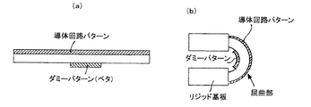
本発明にかかるフレックスリジッド配線板を構成するフレキシブル基板には、図1および図2に示すように、その屈曲部付近において、導体回路パターンが形成された表面と反対側の表面に電気的接続を行う機能を有しないダミーパターンが形成されている。
このダミーパターンは、電気的な接続を行なう機能を有していないので、必ずしも導体回路パターンと同様の材料から形成される必要がなく、樹脂、セラミック等の絶縁材料から形成してもよい。加工性、形状の均一性保持、折り曲げに対する耐性(耐折性)という観点から、金属からなる材料を用いることが望ましい。
As shown in FIGS. 1 and 2, the flexible substrate constituting the flex-rigid wiring board according to the present invention is electrically connected to the surface opposite to the surface on which the conductor circuit pattern is formed in the vicinity of the bent portion. A dummy pattern having no function to perform is formed.
Since this dummy pattern does not have a function of electrical connection, it is not necessarily formed from the same material as the conductor circuit pattern, and may be formed from an insulating material such as resin or ceramic. From the viewpoints of workability, shape uniformity retention, and resistance to bending (folding resistance), it is desirable to use a metal material.
前記ダミーパターンは、主として、フレキシブル基板の屈曲部を中心としてその周辺に形成することが望ましく、フレキシブル基板を折り曲げた際に、内側となるような表面に形成することがより望ましい。その理由は、屈曲部における屈曲具合(曲率半径)を大きくすることができ、導体回路の断線等を引き起こしにくくして、接続信頼性やヒートサイクル条件下における信頼性低下を防止できるからである。 The dummy pattern is preferably formed mainly around the bent portion of the flexible substrate, and more preferably on the surface that becomes the inner side when the flexible substrate is bent. The reason is that the degree of bending (curvature radius) in the bent portion can be increased, and it is difficult to cause disconnection of the conductor circuit and the like, and connection reliability and reliability deterioration under heat cycle conditions can be prevented.
このように、フレキシブル基板をガラスクロスに樹脂(特に、エポキシ系樹脂)を含浸、乾燥させてなる屈曲可能な基材から形成し、その屈曲部周辺にダミーパターンを配設することによって、前記基材からなるフレキシブル基板に対して、適度な剛性(強度)を付与するだけでなく、屈曲部においては適度な柔軟性を付加することができるので、屈曲部の屈曲具合(曲率半径)を大きくすることができる共に、その屈曲具合を一定に維持することができる。 In this way, the flexible substrate is formed from a bendable base material obtained by impregnating and drying a glass cloth with a resin (particularly an epoxy resin), and a dummy pattern is disposed around the bent portion, whereby the base is formed. Not only can moderate rigidity (strength) be imparted to a flexible substrate made of a material, but also moderate flexibility can be added at the bent portion, so that the bending degree (curvature radius) of the bent portion is increased. In addition, the bending state can be kept constant.
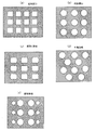
前記ダミーパターンは、図3に示すように、導体層または絶縁層中に、単一あるいは複数種類の形状の開口を有し、それらの複数の開口が少なくとも一列に、規則正しく格子状に配置された格子状パターンに形成されていることが望ましい。
なお、ここでいう「格子状」とは、複数の開口が碁盤目状に配列されている状態(図3(a)〜(c)参照)だけでなく、千鳥状に配列されている状態(図3(d)参照)を含む概念である。
As shown in FIG. 3, the dummy pattern has a single or a plurality of types of openings in the conductor layer or the insulating layer, and the plurality of openings are regularly arranged in a grid pattern in at least one row. It is desirable to form in a lattice pattern.
Here, the “lattice shape” means not only a state in which a plurality of openings are arranged in a grid pattern (see FIGS. 3A to 3C), but also a state in which the openings are arranged in a staggered pattern ( This is a concept including FIG.
また、本発明におけるダミーパターンとしては、複数の開口を有しないベタパターンも含まれるが、フレキシブル基板の屈曲部付近において折り曲げ難くなることが有るし、ヒートサイクルなどの信頼性試験においても、発生した応力が緩衝されないまま伝達される場合があるので、基材や導体回路にダメージを与える場合がある。そのため、ダミーパターンはベタではなく、少なくとも一列に規則正しく配列された複数の開口を有する格子状パターンに形成されることが望ましいのである。 In addition, the dummy pattern in the present invention includes a solid pattern that does not have a plurality of openings, but it may be difficult to bend in the vicinity of the bent portion of the flexible substrate, and has also occurred in reliability tests such as heat cycle. Since the stress may be transmitted without being buffered, it may damage the substrate and the conductor circuit. For this reason, it is desirable that the dummy pattern is not a solid pattern but a lattice pattern having a plurality of openings regularly arranged in at least one row.
前記格子状パターンをなす開口の形状は、三角形、四角形、五角形以上の多角形等の角形状、それらの角部にR部を設けた、即ち、角部を面取りした形状、あるいは円形、楕円形等の曲線形状、もしくは角形状と曲線形状との組合せ形状とすることができる。 The shape of the openings forming the grid pattern is a triangular shape such as a triangle, a quadrangle, a pentagon or more polygon, and the corners are provided with an R portion, that is, a shape in which the corners are chamfered, or a circle or an ellipse. Or a combination of a square shape and a curved shape.
また、前記格子状パターンをなす開口は、同一形状および同一面積に形成してもよいし、異なる形状もしくは異なる面積の組合せにより形成してもよい(図3(e)参照)。 The openings forming the lattice pattern may be formed in the same shape and the same area, or may be formed by different shapes or combinations of different areas (see FIG. 3 (e)).
また、各パターンを形成する複数の開口間の距離(ピッチ)は、一定であってもよいし、不均一であってもよく、さらに、屈曲部付近だけ開口形状の大きさやピッチを変化させてもよい。
図3(a)〜(e)に示すようなパターンにより形成することがより望ましい。
Further, the distance (pitch) between the plurality of openings forming each pattern may be constant or non-uniform, and the size or pitch of the opening shape is changed only in the vicinity of the bent portion. Also good.
It is more desirable to form the pattern as shown in FIGS.
前記各パターンを形成する各開口の面積は、10000〜200000μm2であることが望ましい。その理由は、10000mm2未満では、フレキシブル部自体が強固になりすぎてしまって、屈曲部の折り曲げを助長することができないと共に、ヒートサイクルなどの信頼性試験においても、発生した応力が伝達しやすくなり、その応力が緩衝されないので、基材や導体回路にダメージを与えてしまうからであり、一方、200000mm2を超えると、屈曲部において基材のウネリが形成され、導体回路が位置ズレしたり、屈曲部分の屈曲具合(曲率半径)を大きく、かつ一定に維持しにくくなるからである。 The area of each opening forming each pattern is preferably 10,000 to 200,000 μm 2 . The reason is that if it is less than 10000 mm 2 , the flexible part itself becomes too strong to facilitate bending of the bent part, and the generated stress is easily transmitted even in reliability tests such as heat cycle. This is because the stress is not buffered and damages the base material and the conductor circuit. On the other hand, if it exceeds 200000 mm 2 , undulation of the base material is formed at the bent portion, and the conductor circuit is misaligned. This is because the bending condition (curvature radius) of the bent portion is large and difficult to keep constant.
また、上記各パターンを形成する各開口の面積の総和と、残りのパターン部分の面積との比が、1:9〜9:1の範囲であることが望ましい。その理由は、1:9未満では、フレキシブル部自体が強固になりすぎ、屈曲部の折り曲げを助長することができないと共に、ヒートサイクルなどの信頼性試験においても、発生した応力が伝達しやすくなり、その応力が緩衝されないので、基材や導体回路にダメージを与えてしまうからである。一方、9:1を越えると、屈曲部に基材のウネリが形成されるので、屈曲具合(曲率半径)を大きく、かつ一定に維持しにくくなるからである。 Moreover, it is desirable that the ratio of the sum of the areas of the openings forming the patterns to the area of the remaining pattern portions is in the range of 1: 9 to 9: 1. The reason is that if it is less than 1: 9, the flexible part itself becomes too strong, and it is not possible to promote bending of the bent part, and the generated stress is easily transmitted even in reliability tests such as heat cycle, This is because the stress is not buffered and damages the base material and the conductor circuit. On the other hand, if the ratio exceeds 9: 1, undulation of the base material is formed in the bent portion, so that it is difficult to keep the bending condition (curvature radius) large and constant.
上記各パターンを形成する各開口の面積の総和と、残りのパターン部分の面積との比が、2:8〜8:2の範囲であることがより望ましい。その範囲であれば、部分的に開口面積の総和と残りのパターン部分の面積との比にバラツキを生じたとしても、ヒートサイクルなどの信頼性試験においても、前述のような問題を引き起こさないし、屈曲部のウネリが形成されることがないので、屈曲具合(曲率半径)を大きく、かつ一定に維持することができるのである。 It is more desirable that the ratio of the total area of the openings forming the patterns to the area of the remaining pattern portions is in the range of 2: 8 to 8: 2. If it is within that range, even if there is some variation in the ratio of the total area of the openings and the area of the remaining pattern part, the reliability test such as heat cycle will not cause the above-mentioned problems. Since no undulation of the bent portion is formed, the degree of bending (curvature radius) can be kept large and constant.
また、上記各パターンを形成する各開口の面積の総和と、残りのパターン部分の面積との比が、9:10〜11:10の範囲であることがより望ましい。その範囲であれば、開口面積の総和と残りのパターン部分の面積との比にバラツキが生じたり、フレキシブル基板におけるバラツキが生じたとしても、確実に信頼性試験に耐えることができるので、屈曲具合(曲率半径)を一様に大きくし、かつ一定に維持することができるのである。 In addition, it is more preferable that the ratio of the total area of the openings forming the patterns to the area of the remaining pattern portions is in the range of 9:10 to 11:10. Within that range, even if there is a variation in the ratio of the total opening area to the remaining pattern area, or even if there is a variation in the flexible substrate, the reliability test can be reliably performed. The (curvature radius) can be increased uniformly and kept constant.
上記各開口の面積が、10000〜126000μm2であることがより望ましく、かつ、各開口の面積の総和と、開口が形成されていない残りのパターン部分の面積との比が、1:9〜9:1の範囲であることがより望ましい。この範囲であれば、形成される形状などに関わらず、フレキシブル部に対する屈曲部の屈曲具合(曲率半径)を大きく、かつ一定に維持することが容易となる。また、位置ズレなどによる電気的な接続不良を低減し、ヒートサイクルなどの信頼性試験においても、応力が緩衝されるので、基材や導体回路にダメージを与えることがなく、信頼性を大幅に向上させることができるからである。 The area of each opening is more preferably 10000 to 126000 μm 2 , and the ratio of the total area of each opening to the area of the remaining pattern portion where no opening is formed is 1: 9 to 9 More desirably, the ratio is in the range of 1: 1. If it is this range, it will become easy to maintain the bending condition (curvature radius) of the bending part with respect to a flexible part large and constant irrespective of the shape etc. which are formed. In addition, electrical connection failures due to misalignment, etc. are reduced, and stress is buffered even in reliability tests such as heat cycle, so there is no damage to the substrate or conductor circuit, greatly improving reliability. This is because it can be improved.
また、上記各開口の面積は、10000〜126000μm2であり、かつ、各開口の面積の総和と、開口が形成されていない残りのパターン部分の面積との比が、9:10〜11:10の範囲であることがより望ましい。この範囲であれば、開口などのバラツキや材料のバラツキによる因子の影響を受けることがなく、信頼性などの面でも安定させることができるからである。 The area of each opening is 10000 to 126000 μm 2 , and the ratio of the total area of each opening to the area of the remaining pattern portion where no opening is formed is 9:10 to 11:10. It is more desirable to be in the range. This is because, within this range, there is no influence of factors such as variations in apertures or material variations, and stability can be achieved in terms of reliability.
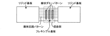
本発明において、ダミーパターンは、図4に示すように、導体回路の配線パターンに対して交差するような方向に延設されたパターンであることが望ましく、そのダミーパターンは、図5(a)および(b)に示すように、フレキシブル基板の屈曲部付近に配設され、少なくとも3本以上の線状パターンからなり、その線幅は150μm以上であることが望ましい。3本以上であると、屈曲部での屈曲具合(曲率半径)を大きく、かつ一定に維持しやすく、線幅が150μm未満であると、屈曲部における屈曲具合(曲率半径)が一定に維持できなくなるからである。 In the present invention, the dummy pattern is desirably a pattern extending in a direction intersecting the wiring pattern of the conductor circuit as shown in FIG. 4, and the dummy pattern is shown in FIG. And as shown in (b), it is disposed near the bent portion of the flexible substrate, is composed of at least three linear patterns, and the line width is preferably 150 μm or more. If the number is 3 or more, the bending state (curvature radius) at the bent portion is large and easy to maintain, and if the line width is less than 150 μm, the bending state (curvature radius) at the bent portion can be maintained constant. Because it disappears.
また、前記線状パターンは、その線間距離が30μm以上であることが望ましく、それによって、フレキシブル基板の屈曲部に沿って延設された線状パターンを並置することができる。30μm未満では、延設されたパターン同士が重なりあうことがあり、それによって、局所的にウネリが形成されるので、導体回路の配線パターンが断線し、接続信頼性を低下させてしまうからである。 The linear pattern preferably has a line-to-line distance of 30 μm or more, whereby the linear patterns extending along the bent portion of the flexible substrate can be juxtaposed. If the thickness is less than 30 μm, the extended patterns may overlap each other, and as a result, undulation is locally formed. Therefore, the wiring pattern of the conductor circuit is disconnected and connection reliability is lowered. .
また、前記線状パターンは、厚みが導体回路の配線パターンの厚みと同等、あるいはそれよりも厚いことが望ましい。その理由は、線状パターンの厚みが導体回路の配線パターンの厚みよりも薄い場合には、フレキシブル基板の屈曲時の屈曲具合(曲率半径)が小さくなってしまう。また、フレキシブル基板の頻繁な屈曲により、導体回路の配線パターンが破断することがあるからである。 The linear pattern preferably has a thickness equal to or greater than the thickness of the wiring pattern of the conductor circuit. The reason is that when the thickness of the linear pattern is thinner than the thickness of the wiring pattern of the conductor circuit, the bending condition (curvature radius) when the flexible substrate is bent becomes small. Further, the wiring pattern of the conductor circuit may be broken due to frequent bending of the flexible substrate.
また、前記線状パターンは、図5(c)に示すように、その断面形状が台形であることが望ましい。その理由は、断面形状が台形であると、ダミーパターンが折り曲げられた場合に、パターン部分が重なりあうことがないので、屈曲部において、段差が形成されることがなく、導体回路の配線パターンの断線が防止されるからである(図5(d)参照)。 The linear pattern preferably has a trapezoidal cross-sectional shape as shown in FIG. The reason is that when the dummy pattern is bent when the cross-sectional shape is trapezoidal, the pattern portions do not overlap, so that no step is formed at the bent portion, and the wiring pattern of the conductor circuit is not formed. This is because disconnection is prevented (see FIG. 5D).
さらに、図5(e)に示すような断面台形であるダミーパターンの台形部分の裾角度は、45〜90°であることが望ましい。屈曲部において延設されたパターンを並置することが容易になるからである。台形部分の裾角度45°未満の場合には、折り曲げた際、延設されたパターンが重なりにくくなる。つまり、隣り合う延設されたパターンの隙間が形成されやすくなるために、屈曲率を一定にし難くなることがある。90°を越えた場合には、隣り合う延設されたパターンの重なりやすくなるために、屈曲率を一定にし難くなることがある。また、それを回避するために、配線同士の距離を大きくさせると、延設されたパターンの隙間が形成されやすくなるために、屈曲率を一定にし難くなることがある。 Furthermore, the skirt angle of the trapezoidal portion of the dummy pattern having a trapezoidal cross section as shown in FIG. 5 (e) is preferably 45 to 90 °. This is because it becomes easy to juxtapose the patterns extended in the bent portion. When the skirt angle of the trapezoidal part is less than 45 °, the extended patterns are difficult to overlap when bent. That is, since it becomes easy to form a gap between adjacent extended patterns, it may be difficult to make the bending rate constant. If the angle exceeds 90 °, the adjacent extended patterns are likely to overlap each other, and it may be difficult to keep the bending rate constant. In order to avoid this, if the distance between the wirings is increased, a gap between the extended patterns is likely to be formed, and it may be difficult to make the bending rate constant.
なお、上記「線状パターン」の概念としては、導体回路の配線パターンと交差するような方向、言い換えれば、フレキシブル基板の屈曲部の屈曲線に沿った方向に設けられた連続した線状パターンだけでなく、四角形、円形、楕円形等の小パターンが所定の間隔をおいて、フレキシブル基板の屈曲部の屈曲線に沿った方向に列設され、全体として線状パターンと同様の機能を果たすようなドットパターンを含んでいる。 The concept of the above “linear pattern” is only a continuous linear pattern provided in a direction intersecting the wiring pattern of the conductor circuit, in other words, in a direction along the bent line of the bent portion of the flexible substrate. Rather, small patterns such as quadrangle, circle, ellipse, etc. are arranged in a direction along the bend line of the bent portion of the flexible substrate at a predetermined interval so as to perform the same function as the linear pattern as a whole. Contains a simple dot pattern.
本発明において、屈曲可能なフレキシブル基板上に形成した導体回路を被覆するカバーレイは、可撓性を有する樹脂付き銅箔、可撓性を有するソルダーレジスト層、またはガラスクロスにエポキシ系樹脂を含浸、乾燥させた後、半硬化させてなるプリプレグから形成されることが望ましい。その理由は、絶縁信頼性、接続信頼性がポリイミドフィルム(例えば、接着剤付きポリイミド)を使用する場合よりも向上するからである。 In the present invention, a coverlay covering a conductor circuit formed on a flexible substrate that can be bent is impregnated with a flexible copper foil with resin, a flexible solder resist layer, or a glass cloth with an epoxy resin. It is desirable to form a prepreg which is dried and then semi-cured. The reason is that insulation reliability and connection reliability are improved as compared with the case of using a polyimide film (for example, polyimide with adhesive).
前記可撓性を有する樹脂付き銅箔は、それを形成する樹脂自体の厚みが50μm前後であることが望ましい。その理由は、絶縁信頼性を確保するためである。
また、前記可撓性を有するソルダーレジスト層は、主として、熱硬化性樹脂、熱可塑性樹脂、感光性を有する樹脂、熱硬化性樹脂の一部分に(メタ)アクリル基を有する樹脂などを用いて形成することができ、ソルダーレジスト層の厚みは、20〜50μmであることが望ましい。その理由は、絶縁信頼性を確保するためである。
さらに、前記ガラスクロスにエポキシ系樹脂を含浸、乾燥させた後、半硬化させてなるプリプレグは、厚みが20〜50μmであることが望ましい。その理由は、絶縁信頼性を確保するためである。
The flexible resin-coated copper foil preferably has a resin itself forming a thickness of about 50 μm. The reason is to ensure insulation reliability.
The flexible solder resist layer is mainly formed using a thermosetting resin, a thermoplastic resin, a photosensitive resin, a resin having a (meth) acryl group in a part of the thermosetting resin, or the like. The thickness of the solder resist layer is preferably 20 to 50 μm. The reason is to ensure insulation reliability.
Further, it is desirable that the prepreg obtained by impregnating and drying an epoxy resin on the glass cloth and then semi-curing it has a thickness of 20 to 50 μm. The reason is to ensure insulation reliability.
本発明を構成するリジット基板は、柔軟性のあるフレキシブル基板と反対に、柔軟性のない基板であり、その形態、層数、形成方法等には関係なく、硬質で容易に変形しないような基板である。 The rigid substrate constituting the present invention is a substrate that is not flexible, contrary to a flexible flexible substrate, and is rigid and does not easily deform regardless of its form, number of layers, formation method, etc. It is.
このリジッド基板において、基板を形成する絶縁性樹脂基材としては、ガラス布エポキシ樹脂基材、ガラス布ビスマレイミドトリアジン樹脂基材、ガラス布ポリフェニレンエーテル樹脂基材、アラミド不織布−エポキシ樹脂基材、アラミド不織布−ポリイミド樹脂基材から選ばれる硬質基材が用いることが好ましく、ガラス布エポキシ樹脂基材がより好ましい。 In this rigid substrate, as the insulating resin base material forming the substrate, glass cloth epoxy resin base material, glass cloth bismaleimide triazine resin base material, glass cloth polyphenylene ether resin base material, aramid nonwoven fabric-epoxy resin base material, aramid It is preferable to use a hard substrate selected from a nonwoven fabric-polyimide resin substrate, and a glass cloth epoxy resin substrate is more preferable.
前記絶縁性樹脂基材の厚さは、20〜600μm程度とする。その理由は、20μm未満の厚さでは、強度が低下して取扱が難しくなるとともに、電気的絶縁性に対する信頼性が低くなり、600μmを超えると微細なビア形成および導電性物質の充填が難しくなるとともに、基板そのものが厚くなるためである。 The insulating resin base material has a thickness of about 20 to 600 μm. The reason is that when the thickness is less than 20 μm, the strength is lowered and handling becomes difficult, and the reliability with respect to the electrical insulation is lowered. When the thickness exceeds 600 μm, it is difficult to form fine vias and fill with a conductive material. At the same time, the substrate itself becomes thick.
かかる絶縁性樹脂基材の片面または両面には銅箔が貼付され、その厚さは、5〜18μm程度とする。その理由は、後述するようなレーザ加工を用いて、絶縁性樹脂基材にビア形成用の開口を形成する際に、薄すぎると貫通してしまうからであり、逆に厚すぎるとエッチングにより、微細な線幅の導体回路パターンを形成し難いからである。 Copper foil is affixed to one or both sides of such an insulating resin base material, and the thickness is about 5 to 18 μm. The reason is that, when using laser processing as will be described later, when forming an opening for forming a via in an insulating resin base material, if it is too thin, it penetrates. This is because it is difficult to form a conductor circuit pattern having a fine line width.
前記絶縁性樹脂基材および銅箔にて構成されるリジッド基板は、特に、エポキシ樹脂をガラスクロスに含浸させてBステージとしたプリプレグと、銅箔とを積層して加熱プレスすることにより得られる片面銅張積層板を用いることができる。このようなリジッド基板は、銅箔がエッチングされた後の取扱中に、配線パターンやビア位置がずれることがなく、位置精度に優れている。 The rigid substrate composed of the insulating resin base material and the copper foil is obtained by, in particular, laminating a prepreg in which a glass cloth is impregnated with a glass cloth and forming a B stage, and a copper foil, followed by hot pressing. A single-sided copper-clad laminate can be used. Such a rigid substrate is excellent in positional accuracy because the wiring pattern and via positions are not shifted during handling after the copper foil is etched.
なお、このリジッド基板の片面または両面に形成される前記導体回路は、厚さが5〜18μm程度の銅箔を、半硬化状態を保持された樹脂接着剤層を介して加熱プレスした後、適切なエッチング処理をすることによって形成されたものが好ましい。 In addition, the conductor circuit formed on one or both sides of the rigid substrate is appropriately pressed after hot pressing a copper foil having a thickness of about 5 to 18 μm through a resin adhesive layer kept in a semi-cured state. What was formed by performing an etching process is preferable.
そして、その導体回路は、基材表面に貼り付けられた銅箔上に、エッチング保護フィルムを貼付けて、所定の回路パターンのマスクで披覆した後、エッチング処理を行って、電極パッド(ビアランド)を含んで形成されたものが好適である。 Then, the conductor circuit is formed by applying an etching protective film on a copper foil affixed to the surface of the base material, displaying it with a mask having a predetermined circuit pattern, and performing an etching process to obtain an electrode pad (via land). Those formed by including are suitable.
こうした導体回路形成工程においては、先ず、銅箔の表面に感光性ドライフィルムレジストを貼付した後、所定の回路パターンに沿って露光、現像処理してエッチングレジストを形成し、エッチングレジスト非形成部分の金属層をエッチングして、電極パッドを含んだ導体回路パターンとする。 In such a conductor circuit forming step, first, after a photosensitive dry film resist is applied to the surface of the copper foil, an etching resist is formed by exposing and developing along a predetermined circuit pattern. The metal layer is etched to form a conductor circuit pattern including electrode pads.
前記処理工程において、エッチング液としては、硫酸一過酸化水素、過硫酸塩、塩化第二銅、塩化第二鉄の水溶液から選ばれる少なくとも1種の水溶液を用いることができる。 In the treatment step, as the etching solution, at least one aqueous solution selected from an aqueous solution of sulfuric acid monohydrogen peroxide, persulfate, cupric chloride, and ferric chloride can be used.
また、前記銅箔をエッチングして導体回路を形成する前処理として、ファインパターンを形成しやすくするため、あらかじめ、銅箔の表面全面をエッチングして厚さを1〜10μm、より好ましくは2〜8μm程度まで薄くすることができる。 Moreover, as a pretreatment for etching the copper foil to form a conductor circuit, in order to easily form a fine pattern, the entire surface of the copper foil is etched in advance to have a thickness of 1 to 10 μm, more preferably 2 to 2 μm. The thickness can be reduced to about 8 μm.
前記リジッド基板に形成される接続用電極パッドは、その形状、大きさ、および個数は、特に限定されないが、たとえば、直径が50〜500μm程度の円形とし、100〜700μm程度のピッチで複数配設することが望ましい。その理由は、50μm未満では、接続信頼性に不安があり、500μmを超えると、高密度実装に不利であるからである。 The shape, size, and number of connection electrode pads formed on the rigid substrate are not particularly limited. For example, a plurality of connection electrode pads having a diameter of about 50 to 500 μm and a pitch of about 100 to 700 μm are arranged. It is desirable to do. The reason is that if it is less than 50 μm, the connection reliability is uneasy, and if it exceeds 500 μm, it is disadvantageous for high-density mounting.
前記絶縁性樹脂基材に、ビアホール形成用の開口(以下、「ビア開口」という)を設ける。このビア開口は、レーザ照射によって形成することができる。特に、絶縁性樹脂基材の表面に透明な保護フィルム、たとえばPETフィルムを貼付し、そのPETフィルムの上方から炭酸ガスレーザ照射を行ない、PETフィルムを貫通して、絶縁性樹脂基材の表面から銅箔に達する開口を形成する。このような加工条件によるビア開口径は、50〜250μm程度であることが望ましい。
なお、レーザ照射によって形成されたビア開口の側面および底面に残留する樹脂残滓を除去するために、デスミア処理を行う。このデスミア処理は、酸素プラズマ放電処理、コロナ放電処理、紫外線レーザ処理またはエキシマレーザ処理等によって行う。
An opening for forming a via hole (hereinafter referred to as “via opening”) is provided in the insulating resin base material. This via opening can be formed by laser irradiation. In particular, a transparent protective film, such as a PET film, is applied to the surface of the insulating resin base material, carbon dioxide laser irradiation is performed from above the PET film, penetrates the PET film, and copper is applied from the surface of the insulating resin base material. An opening reaching the foil is formed. The via opening diameter under such processing conditions is desirably about 50 to 250 μm.
A desmear process is performed in order to remove the resin residue remaining on the side and bottom surfaces of the via opening formed by laser irradiation. This desmear treatment is performed by oxygen plasma discharge treatment, corona discharge treatment, ultraviolet laser treatment, excimer laser treatment, or the like.
前記ビア開口には導電性物質が充填されて、充填ビアホールが形成されるが、その導電性物質としては、導電性ペーストや電解めっき処理によって形成される金属めっきが好ましい。
前記充填ビアホールの形成工程をシンプルにして、製造コストを低減させ、歩留まりを向上させる点では、導電性ペーストの充填が好ましく、接続信頼性の点では電解めっき処理によって形成される金属めっきが好ましく、とくに、電解銅めっきが好適である。
The via opening is filled with a conductive material to form a filled via hole. The conductive material is preferably a conductive paste or metal plating formed by electrolytic plating.
In terms of simplifying the formation process of the filled via hole, reducing the manufacturing cost, and improving the yield, filling with a conductive paste is preferable, and in terms of connection reliability, metal plating formed by electrolytic plating is preferable, In particular, electrolytic copper plating is suitable.
前記導電性物質は、絶縁性基材を貫通し導体回路に達するビア開口内に充填されるだけでなく、ビア開口の外側に所定の高さまで突出形成することもでき、その突出高さは5〜30μm程度の範囲が望ましい。
その理由は、5μm未満では、接続不良を招きやすく、30μmを越えると抵抗値が高くなると共に、加熱プレス工程において熱変形した際に、絶縁性基板の表面に沿って拡がりすぎるので、ファインパターンが形成できなくなるからである。
The conductive material not only fills the via opening that penetrates the insulating base material and reaches the conductor circuit, but also protrudes to a predetermined height outside the via opening, and the protruding height is 5 A range of about 30 μm is desirable.
The reason is that if the thickness is less than 5 μm, it is easy to cause a connection failure. If the thickness exceeds 30 μm, the resistance value becomes high, and when it is thermally deformed in the hot press process, it spreads too much along the surface of the insulating substrate. It is because it becomes impossible to form.
本発明において、リジッド基板とフレキシブル基板との電気的接続は、以下の(1)〜(4)のような種々の形態を採用することができ、これらの接続形態を任意に組合せることによって、基板材料を有効に使用することができると共に、自由な配線接続構造とすることができる。 In the present invention, the electrical connection between the rigid substrate and the flexible substrate can adopt various forms such as the following (1) to (4), and by arbitrarily combining these connection forms, A substrate material can be used effectively, and a free wiring connection structure can be provided.
(1) リジッド基板の片面にフレキシブル基板を接続する場合、すなわち、リジッド基板の片方の最外層の表面に接続用電極パッドを形成すると共に、フレキシブル基板の片方の表面にも接続用電極パッドを形成し、各基板の電極パッド同士を、塊状導電体などを介して接続させる。 (1) When connecting a flexible board to one side of a rigid board, that is, forming a connection electrode pad on the outermost surface of one side of the rigid board, and forming a connection electrode pad on one side of the flexible board Then, the electrode pads of each substrate are connected to each other through a block conductor.
(2) リジッド基板の両面に、異なるフレキシブル基板をそれぞれ接続する場合、すなわち、リジッド基板の両方の最外層の表面に接続用電極パッドをそれぞれ形成すると共に、各フレキシブル基板をリジッド基板の両方の最外層に形成した接続用電極パッドに対面して配置させ、それらの対面配置された接続用電極パッド同士を塊状導電体を介して接続させる。 (2) When different flexible boards are connected to both sides of the rigid board, that is, connecting electrode pads are formed on the surfaces of both outermost layers of the rigid board, and each flexible board is attached to the uppermost of both of the rigid boards. The connection electrode pads formed on the outer layer are arranged to face each other, and the connection electrode pads arranged to face each other are connected to each other through a block conductor.
(3) フレキシブル基板の両面に、異なるリジッド基板をそれぞれ接続する場合、すなわち、フレキシブル基板の両面に接続用電極パッドを形成すると共に、それらの接続用電極パッドに対して、片方の最外層の表面に接続用電極パッドがそれぞれ形成された異なるリジッド基板を、それらの基板の各接続用電極パッドがそれぞれ対面するように配置させ、対面配置された接続用電極パッド同士を塊状導電体を介して接続させる。 (3) When connecting different rigid boards to both sides of the flexible board, that is, forming connection electrode pads on both sides of the flexible board, and the surface of one outermost layer with respect to those connection electrode pads Different rigid substrates each having connection electrode pads formed thereon are arranged so that the connection electrode pads of the substrates face each other, and the connection electrode pads arranged face to face are connected to each other via a block conductor Let
(4) フレキシブル基板の複数箇所において、リジッド基板の複数が電気的接続される形態であり、複数のリジッド基板は、それらを構成する導体層および樹脂絶縁層の層数が任意であるように予め形成され、それらの個別に形成されたリジッド基板とフレキシブル基板の接続用電極パッドを対向して配置し、それらの対向配置された接続用電極パッド同士を、塊状導電体を介して接続させる。 (4) A plurality of rigid substrates are electrically connected at a plurality of locations on the flexible substrate, and the plurality of rigid substrates are preliminarily arranged so that the number of conductor layers and resin insulating layers constituting them is arbitrary. The individually formed rigid board and flexible board connecting electrode pads are arranged to face each other, and the connecting electrode pads arranged to face each other are connected to each other through a block conductor.
ここで、前記(1)〜(4)の種々の接続形態の中で、特に、(4)に記載されたような、リジッド基板の片方の最外層表面においてフレキシブル基板が接続される形態について、説明する。 Here, among the various connection forms of (1) to (4), in particular, as described in (4), the form in which the flexible substrate is connected on the outermost surface of one of the rigid substrates, explain.
たとえば、フレキシブル基板の一方の端部において、その片面あるいは両面に対して予め層間接続されたリジッド基板が接合され(一方の「リジッド部」という)、フレキシブル基板の片方の端部においても、その片面あるいは両面に対して、予め層間接続された他のリジッド基板が接合されている(他方の「リジッド部」という)形態が代表的である。 For example, at one end of a flexible substrate, a rigid substrate that is interlayer-connected in advance to one surface or both surfaces thereof is joined (referred to as one “rigid portion”), and at one end of the flexible substrate, the single surface Alternatively, a form in which another rigid substrate that has been interlayer-connected in advance is bonded to both surfaces (referred to as the other “rigid portion”) is representative.
このような接続形態では、フレキシブル基板の両端部間の部分は、リジッド基板との接触がない部分(「フレキシブル部」という)であり、このフレキシブル部には、一方のリジッド部と他方のリジッド部とを電気的接続する導体回路が設けられており、このような導体回路は通常、カバーレイと呼ばれる絶縁層によって被覆されている。 In such a connection form, a portion between both end portions of the flexible substrate is a portion that is not in contact with the rigid substrate (referred to as a “flexible portion”). The flexible portion includes one rigid portion and the other rigid portion. A conductor circuit that electrically connects the two is provided, and such a conductor circuit is usually covered with an insulating layer called a coverlay.
各リジッド部を構成するフレキシブル基板の片面の所定領域、たとえば、細長い矩形状の基板の短辺に沿った表面領域には、導体回路の一部として複数の接続用電極パッドが予め形成されるとともに、導体回路や絶縁層が予め積層形成され、かつ層間接続されたリジッド基板の外側表面の所定領域にも、フレキシブル基板に設けた接続用電極パッドに対応した複数の接続用電極パッドが予め形成される。
各リジッド部におけるこれらの複数の接続用電極パッド対は、リジッド基板とフレキシブル基板との間に介在させた塊状導電体によって電気的に接続されると共に、接続用電極パッド以外の表面領域においては、接着剤によって接着されるように一体形成される。
A plurality of connection electrode pads are formed in advance as part of the conductor circuit in a predetermined region on one side of the flexible substrate constituting each rigid portion, for example, a surface region along the short side of the elongated rectangular substrate. In addition, a plurality of connection electrode pads corresponding to the connection electrode pads provided on the flexible substrate are also formed in advance on a predetermined region on the outer surface of the rigid substrate that is preliminarily laminated with a conductor circuit and an insulating layer. The
The plurality of connection electrode pad pairs in each rigid portion are electrically connected by a bulky conductor interposed between the rigid substrate and the flexible substrate, and in a surface region other than the connection electrode pads, It is integrally formed so that it may adhere | attach with an adhesive agent.
前記接続用電極パッドは、リジッド基板の最外層を構成する回路基板の一つあるいは二つに対して、めっき処理またはエッチング処理によって導体回路を形成する際に、その導体回路の一部として形成されることができるが、最外層を構成する回路基板の絶縁樹脂層上に単独で形成されてもよいし、その絶縁樹脂層を貫通して下層の導体回路との電気的接続を行なうバイアホールランドとして形成することもできる。 The connection electrode pad is formed as a part of a conductor circuit when the conductor circuit is formed by plating or etching on one or two of the circuit boards constituting the outermost layer of the rigid board. However, the via hole land may be formed independently on the insulating resin layer of the circuit board constituting the outermost layer, or may be electrically connected to the underlying conductor circuit through the insulating resin layer. Can also be formed.
本発明において、前記リジッド基板に形成される接続用電極パッドの形成領域は、必ずしもリジッド基板の最外層の絶縁樹脂層表面の全域である必要はなく、十分な接続強度が得られるような任意の位置であればよい。
たとえば、矩形状の基板の短辺あるいは長辺に沿った周縁の表面領域や、基板の周縁から中央に向う表面領域であってもよい。
In the present invention, the formation region of the connection electrode pad formed on the rigid substrate does not necessarily need to be the entire surface of the insulating resin layer surface of the outermost layer of the rigid substrate, and may be an arbitrary one that provides sufficient connection strength. Any position is acceptable.
For example, it may be a peripheral surface region along a short side or a long side of a rectangular substrate, or a surface region from the peripheral edge of the substrate toward the center.
このような接続用電極パッドの形成領域を任意の位置とすることができるので、電子機器筐体のデザインや、その筐体内に収容される他のリジッド基板や電子部品等のレイアウトに応じて、所望の方向に配線の引き出しが可能となり、極めて有利な配線接続構造を得ることができる。 Since the formation region of such a connection electrode pad can be at an arbitrary position, depending on the design of the electronic device casing and the layout of other rigid boards and electronic components accommodated in the casing, Wiring can be drawn out in a desired direction, and an extremely advantageous wiring connection structure can be obtained.
さらに、前記リジッド基板とフレキシブル基板とは、リジッド基板側あるいはフレキシブル基板側の接続用電極パッドが形成されていない表面領域に貼付または塗布形成された絶縁性接着剤層によって接着される。 Further, the rigid substrate and the flexible substrate are bonded to each other by an insulating adhesive layer that is affixed or applied to the surface region where the connection electrode pads on the rigid substrate side or the flexible substrate side are not formed.
本発明において、リジッド基板の層間接続部の位置とフレキシブル基板の層間接続部の位置とを一致させ、これらの層間接続部同士を塊状導電体を介して重ね合わせて導通させたスタック構造部を形成することが、より好ましい実施の形態であり、そのようなスタック構造の採用によって、配線長の短縮化を実現して、大電力が必要な電子部品の実装に好適なフレックスリジッド配線板を提供することができる。 In the present invention, the position of the interlayer connection portion of the rigid substrate is matched with the position of the interlayer connection portion of the flexible substrate, and a stack structure portion is formed in which these interlayer connection portions are overlapped with each other via a block conductor to conduct. This is a more preferred embodiment, and by adopting such a stack structure, the wiring length is shortened, and a flex-rigid wiring board suitable for mounting electronic components that require high power is provided. be able to.
前記リジッド基板およびフレキシブル基板に設けた接続用電極パッド同士を接続する塊状導電体は、リジッド基板もしくはフレキシブル基板のいずれか一方の接続用電極パッド上に突設した形態であることが好ましい。リジッド基板とフレキシブル基板とを重ね合わせる際に、絶縁性接着剤層を貫通しやすいからである。 It is preferable that the bulky conductor for connecting the connection electrode pads provided on the rigid substrate and the flexible substrate protrudes on one of the connection electrode pads of the rigid substrate or the flexible substrate. This is because when the rigid substrate and the flexible substrate are overlapped, it is easy to penetrate the insulating adhesive layer.
前記塊状導電体としては、銅、金、銀、スズ等の金属、それらの合金、あるいは種々の半田等を用いて、めっきや、印刷法、転写法、埋め込み法(インプラント)、電着等の手法によって、球状や半球状等の滑らかな凸曲面形状、角柱や円柱等の柱状、あるいは角錐や円錐等の錐状に形成されたバンプ(ポスト)やボール、あるいはピン形状に形成されたものが代表的であるが、これらに限定されるべきものではなく、リジッド基板に設けた接続用電極パッドとフレキシブル基板に設けた接続用電極パッドとを十分な接続強度で接続し、かつ電気的接続できる手段であればよい。 Examples of the bulk conductors include metals such as copper, gold, silver, tin, alloys thereof, various solders, plating, printing, transfer, embedding (implant), electrodeposition, etc. Depending on the method, there are bumps (posts), balls, or pins formed into smooth convex curved shapes such as spherical and hemispherical shapes, prismatic shapes such as prisms and cylinders, or conical shapes such as pyramids and cones. Typically, but not limited thereto, the connection electrode pad provided on the rigid substrate and the connection electrode pad provided on the flexible substrate can be connected with sufficient connection strength and can be electrically connected. Any means may be used.
前記バンプ(ポスト)をめっきによって形成する場合には、銅めっきにより形成したものであってもよく、そのような塊状導電体は、フレキシブル基板に設けた接続用電極パッドに対して半田層を介して接続されることが好ましく、それによって優れた電気的接続性が得られる。 When the bumps (posts) are formed by plating, the bumps (posts) may be formed by copper plating, and such a bulky conductor is connected to a connection electrode pad provided on a flexible substrate via a solder layer. Are preferably connected so that excellent electrical connectivity is obtained.
また、前記バンプ(ポスト)やボールを形成する半田としては、Sn/Pb、Sn/Sb、Sn/Ag、Sn/Ag/Cu、Sn/Cu、Sn/Zn、Sn/Ag/In/Cuから選ばれる少なくとも一種の半田から形成することができる。
すなわち、前記金属あるいは各種半田の中から選ばれる1種類で形成してもよいし、2種類以上を混合して用いてもよい。
特に、自然環境を汚染しないという社会的要請に応じて、鉛を含有しない、いわゆる鉛フリー半田を用いたバンプが好ましい。そのような半田として、たとえばSn/Sb、Sn/Ag、Sn/Ag/Cu、Sn/Cu、Sn/Zn、Sn/Ag/In/Cuからなる半田が挙げられる。リジッド基板やフレキシブル基板の材料を考慮して、融点が183℃であるSn−37Pb半田や、融点が217℃であるSn−35Ag−0.7Cu半田が、より好ましい。
The solder for forming the bump (post) or ball is Sn / Pb, Sn / Sb, Sn / Ag, Sn / Ag / Cu, Sn / Cu, Sn / Zn, Sn / Ag / In / Cu. It can be formed from at least one selected solder.
That is, it may be formed of one kind selected from the metals or various solders, or two or more kinds may be mixed and used.
In particular, a bump using so-called lead-free solder that does not contain lead is preferable in response to a social request not to pollute the natural environment. Examples of such solder include solder composed of Sn / Sb, Sn / Ag, Sn / Ag / Cu, Sn / Cu, Sn / Zn, and Sn / Ag / In / Cu. In consideration of the material of the rigid substrate and the flexible substrate, Sn-37Pb solder having a melting point of 183 ° C. and Sn-35Ag-0.7Cu solder having a melting point of 217 ° C. are more preferable.
さらに、Sn/Ag半田めっきによって形成したバンプは、展性に優れて冷熱サイクルで発生する応力を緩和するのに有効であるため、より好ましい。 Furthermore, a bump formed by Sn / Ag solder plating is more preferable because it has excellent malleability and is effective in relieving the stress generated in the thermal cycle.
前記半田バンプは、その高さが10〜150μm程度であることが好ましく、めっき、印刷法、転写法、埋め込み法(インプラント)、電着等によって形成することができる。
たとえば、印刷法による場合には、接続用電極パッドを有するリジッド基板またはフレキシブル基板の接続用電極パッドに相当する基板上の箇所に、円形の開口を設けた印刷マスク(メタルマスク)を載置し、そのマスクを用いて半田ペーストを印刷し、加熱処理することによって半田バンプを形成する。
The solder bump preferably has a height of about 10 to 150 μm, and can be formed by plating, printing, transfer, embedding (implant), electrodeposition, or the like.
For example, in the case of the printing method, a printing mask (metal mask) having a circular opening is placed at a position on the substrate corresponding to the connection electrode pad of a rigid substrate having a connection electrode pad or a flexible substrate. Then, solder paste is printed using the mask, and solder bumps are formed by heat treatment.
また、転写法による場合には、たとえば、水平面を有する水平治具板の当該水平面上に、接続用電極パッドを有するリジッド基板またはフレキシブル基板、半田キャリアおよび荷重用の押さえ治具を順次載置して、水平治具板と押さえ治具とにより基板および半田キャリアを挟持し、両者を平行に保持し、その後、リフローにより半田キャリアの半田パターンを接続用電極パッド上に転写し、その後、半田キャリアを取り除くことで、接続用電極パッド上に半田バンプを形成する。 In the case of the transfer method, for example, a rigid board or a flexible board having connection electrode pads, a solder carrier, and a load holding jig are sequentially placed on the horizontal plane of a horizontal jig plate having a horizontal plane. Then, the substrate and the solder carrier are sandwiched by the horizontal jig plate and the holding jig, and both are held in parallel, and then the solder pattern of the solder carrier is transferred onto the connection electrode pad by reflow, and then the solder carrier As a result, the solder bumps are formed on the connection electrode pads.
さらに、前記半田ボールは、たとえば、直径が100〜800μm程度の銅球と、その銅球を被覆する厚み150μm以下の半田層とから形成してもよい。 Further, the solder ball may be formed of, for example, a copper sphere having a diameter of about 100 to 800 μm and a solder layer having a thickness of 150 μm or less covering the copper sphere.
前記リジッド基板とフレキシブル基板との電気的および物理的接続は、フレキシブル基板の接続用電極パッドをリジッド基板の接続用電極パッド上の半田バンプあるいは半田ボールに対して加圧、加熱して半田を溶融・固化させることによって行なわれることが好ましい。 Electrical and physical connection between the rigid substrate and the flexible substrate is performed by pressing and heating the connection electrode pads of the flexible substrate against the solder bumps or solder balls on the connection electrode pads of the rigid substrate to melt the solder. -It is preferable to carry out by solidifying.
本発明において、リジッド基板とフレキシブル基板とを相互に接着、固定し、かつ前記塊状導電体が貫挿する絶縁性接着剤層をなす樹脂としては、例えば、ポリビニルブチラール樹脂、フェノール樹脂、ニトリルラバー、ポリイミド樹脂、フェノキシ樹脂、キシレン樹脂もしくはこれらの2種以上の混合物、ポリカーボネート樹脂、ポリスルホン樹脂、ポリエーテルイミド樹脂、液晶ポリマー、ポリアミド樹脂なども使用することが可能である。また、前記樹脂にガラスマット、無機充填剤、ガラスクロスなどを配合したもの(プリプレグ)でもよい。 In the present invention, as the resin that forms an insulating adhesive layer for bonding and fixing the rigid substrate and the flexible substrate to each other and through which the massive conductor penetrates, for example, polyvinyl butyral resin, phenol resin, nitrile rubber, Polyimide resin, phenoxy resin, xylene resin or a mixture of two or more of these, polycarbonate resin, polysulfone resin, polyetherimide resin, liquid crystal polymer, polyamide resin, and the like can also be used. Moreover, what mix | blended glass mat, an inorganic filler, glass cloth, etc. with the said resin (prepreg) may be sufficient.
例えば、プリプレグを用いる場合には、リジッド基板とフレキシブル基板との間にプリプレグ等を介在させた状態で、熱プレスすることによって絶縁性接着剤層を形成する。 For example, when a prepreg is used, the insulating adhesive layer is formed by hot pressing with a prepreg or the like interposed between a rigid substrate and a flexible substrate.
前記プリプレグを用いる場合には、接続用電極パッド上に形成するバンプとしては、金属ペーストを所定の形状に成形した後、硬化して形成したバンプであることが好ましく、所定の位置に精度よく貫通型の導体路を形成するために、その先端部が絶縁性接着剤層を容易に貫挿し得るような円錐型、角錐型など好ましいが、半球状、台形などでもよい。 In the case of using the prepreg, the bump formed on the connection electrode pad is preferably a bump formed by forming a metal paste into a predetermined shape and then curing it, and accurately penetrates into a predetermined position. In order to form a conductive path of a mold, a tip shape such as a cone shape or a pyramid shape that can easily penetrate the insulating adhesive layer is preferable, but a hemispherical shape, a trapezoid shape, or the like may be used.
前記金属ペーストは、たとえば銀、金、銅、半田粉、炭素粉などの導電性粉末、これらの合金粉末もしくは複合(混合)金属粉末と、たとえばポリカーボネート樹脂、ポリスルホン樹脂、ポリエステル樹脂、フェノキシ樹脂、メラミン樹脂、フェノール樹脂、ポリイミド樹脂などのバインダー成分とを混合して調製された導電性組成物で構成することができる。 The metal paste includes, for example, conductive powder such as silver, gold, copper, solder powder, carbon powder, alloy powder or composite (mixed) metal powder thereof, and polycarbonate resin, polysulfone resin, polyester resin, phenoxy resin, melamine, for example. It can comprise with the electroconductive composition prepared by mixing binder components, such as resin, a phenol resin, and a polyimide resin.
そして、前記金属バンプは、例えば、比較的厚いメタルマスクを用いた印刷法により、アスペクト比の高い導電性バンプとして形成でき、そのバンプの高さは、絶縁性接着剤層の厚さの1.3倍程度以上が好ましい。例えば、絶縁性接着剤層の厚さを50μmとすると、65〜150μm 程度に設定される。 The metal bumps can be formed as conductive bumps having a high aspect ratio by, for example, a printing method using a relatively thick metal mask, and the height of the bumps corresponds to the thickness of the insulating adhesive layer. About 3 times or more is preferable. For example, when the thickness of the insulating adhesive layer is 50 μm, the thickness is set to about 65 to 150 μm.
なお、フレキシブル基板とリジット基板との電気的な接続は、上述したような、各基板に設けた接続用電極パッド同士を塊状導電体を介して接続させる形態以外にも、フレキシブル基板とリジット基板の重ね合う部分を貫通しためっきスルーホールを形成し、そのめっきスルーホールを介して電気的な接続を行なうような形態でもよい。フレキシブル基板とリジット基板との電気的接続をめっきスルーホールを介して行う形式のフレックスリジッド配線板を製造する方法の一例を、以下に説明する。 In addition, the electrical connection between the flexible substrate and the rigid substrate is not limited to the above-described form in which the connection electrode pads provided on each substrate are connected to each other via the bulk conductor. It is also possible to form a plated through hole penetrating through the overlapping portion and make an electrical connection through the plated through hole. An example of a method for manufacturing a flex-rigid wiring board of a type in which electrical connection between a flexible substrate and a rigid substrate is performed through a plated through hole will be described below.
まず、ガラスクロスにエポキシ系樹脂を含浸、乾燥させてなる絶縁性基材の一方の表面に導体回路の配線パターンを形成し、その配線パターン形成面と反対側の表面には、屈曲部周辺にダミーパターンを形成してなるフレキシブル基板を用意する。 First, a wiring pattern of a conductor circuit is formed on one surface of an insulating base material obtained by impregnating and drying an epoxy resin on a glass cloth, and on the surface opposite to the wiring pattern forming surface, around the bent portion. A flexible substrate formed with a dummy pattern is prepared.
次に、配線パターンおよびダミーパターンが形成された基板の両面を被覆するカバー層を形成し、その基板の両面に対して、屈曲が必要な箇所を開口したプリプレグと、銅箔とを積層した後、加熱プレスすることによって積層体を形成する。 Next, after forming a cover layer that covers both sides of the substrate on which the wiring pattern and the dummy pattern are formed, and laminating a copper foil with a prepreg that opens a portion that needs to be bent on both sides of the substrate The laminate is formed by heating and pressing.
その積層体表面の銅箔にレーザ照射用開口を形成すると共に、所定の照射条件でレーザ照射を行って、基板を貫通する貫通孔を形成した後、貫通孔の内壁を含んだ基板表面に銅めっき層を形成し、めっきスルーホールを形成する。 A laser irradiation opening is formed in the copper foil on the surface of the laminate, and laser irradiation is performed under predetermined irradiation conditions to form a through hole penetrating the substrate, and then copper is formed on the substrate surface including the inner wall of the through hole. A plating layer is formed and a plating through hole is formed.
次いで、銅めっき層を形成した基板の表面および裏面に、エッチング処理により配線パターンを形成すると、めっきスルーホールを介してフレキシブル基板に形成された配線パターンに電気的に接続されることになる。 Next, when a wiring pattern is formed by etching treatment on the front and back surfaces of the substrate on which the copper plating layer is formed, the wiring pattern is electrically connected to the wiring pattern formed on the flexible substrate through the plated through hole.
さらに、ソルダーレジスト層を形成した後、ルーターによる外形加工を行なうことによって、一方の表面に配線パターンが形成され、他方の表面にダミーパターンが形成されてなるフレキシブル部を有するフレックスリジッド配線板を製造することができる。
以下、本発明のフレックスリジッド配線板について、実施例に基づいてさらに詳細に説明する。
Furthermore, after forming the solder resist layer, a flex-rigid wiring board having a flexible part in which a wiring pattern is formed on one surface and a dummy pattern is formed on the other surface is produced by external processing by a router. can do.
Hereinafter, the flex-rigid wiring board of the present invention will be described in more detail based on examples.
(A)フレキシブル基板の製造工程
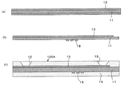
(1) 本発明にかかるフレックスリジッド配線板を製造するに当たって、それを構成するフレキシブル基板100Aを作製する出発材料として、厚さ20μm(厚さ30μm以下のものを用いることができる)のガラスクロス(ガラス繊維の太さ平均4.0μm)にエポキシ系樹脂を含浸、乾燥させてなる絶縁性基材11の両面に、厚さが18μmの銅箔12がラミネートされた厚さ50μmである両面銅張積層板(日立化成:製品名「E−67」)を用いた(図6(a))。
(A) Flexible substrate manufacturing process
(1) In manufacturing a flex-rigid wiring board according to the present invention, a glass cloth having a thickness of 20 μm (thickness of 30 μm or less can be used) is used as a starting material for manufacturing the
(2) 前記絶縁性基材11の両面にラミネートされた銅箔12に対して、塩化第二銅水溶液を用いてエッチング処理を施して、片面に線幅が300μmの導体回路パターン13および直径250μmの接続用電極パッド16を形成し、その導体回路の配線パターン形成面と反対側の表面には、屈曲部周辺に、格子状のダミーパターン18(開口形状が矩形、各開口面積が10000μm2、開口面積の総和:パターン残部面積=10:10)を形成した(図6(b)参照)。
(2) The
(3) 前記配線パターン13を覆って、ソルダーレジスト(日本ポリテック社製:製品名「NPR−90」)をスクリーン印刷により塗布し、乾燥させた後、露光量400mj/cm2で露光し、さらに150℃/1時間の条件で乾燥させることによって、配線パターン13を保護する厚さ20μmの樹脂製カバー層14を形成した(図6(c)参照)。
なお、このカバー層14には、接続用電極パッド16に達する直径300μmの開口15が設けられ、この開口15を介して後述するようなリジッド基板の接続用電極パッドに設けた塊状導電体が、接続用電極パッド16に電気的に接続されるようになっている。
(3) Covering the
The
(B)リジッド基板の製造工程
(1) ガラスエポキシ樹脂からなる基板21の両面に、12μmの銅箔22がラミネートされた厚さ0.11mmの両面銅張積層板(松下電工製:R−1766、図7(a)参照)の片面に塩化第二銅水溶液を用いて、レーザ照射用開口24を形成し、さらに炭酸ガスレーザを用いて直径250μmの銅めっき充填用開口26を設けた(図7(b)、(c)参照)。
(B) Rigid substrate manufacturing process
(1) 0.11 mm thick double-sided copper-clad laminate with 12
(2) さらに、貫通孔26の内壁にPd触媒を付与し、以下のような組成および条件のもとで無電解銅めっき処理を施した後、さらに電解銅めっき処理を施すことによって、開口26の内部を銅めっき28で充填した(図7(d)参照)。
(2) Further, a Pd catalyst is applied to the inner wall of the through-
(無電解銅めっき溶液)
硫酸銅 10g/リトッル
HCHO 8g/リットル
NaOH 5g/リットル
ロッシェル塩 45g/リットル
温度 30℃
(Electroless copper plating solution)
Copper sulfate 10g / Little HCHO 8g / liter NaOH 5g / liter Rochelle salt 45g / liter Temperature 30 ° C
(電解銅めっき溶液)
硫酸 180g/リットル
硫酸銅 80g/リットル
アトテックジャパン製 商品名 カパラシドGL
1ml/リットル
(めっき条件)
電流密度 2A/dm2
時間 30分
温度 25℃
(Electrolytic copper plating solution)
Sulfuric acid 180g / liter Copper sulfate 80g / liter Atotech Japan product name Kaparaside GL
1 ml / liter (plating conditions)
Current density 2A / dm 2
Time 30 minutes Temperature 25 ° C
(3) 前記銅めっき28で充填した基板の両面を塩化第二銅水溶液を用いてエッチングして、表面および裏面にそれぞれパターン32、34を形成すると共に、パターン34の一部を接続用電極パッド36に形成した。さらに、基板をルータで加工した(図7(e)参照)。
(3) Both sides of the substrate filled with the copper plating 28 are etched using a cupric chloride aqueous solution to form
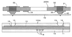
(4) 次いで、円錐形状の開口を設けたメタルマスクを用いて、銀ペースト(DU PONT社製:商品名 SOLAMET)をスキージを用いて充填し、接続用電極パッド36上に円錐形状の突起40、すなわち半田バンプを形成した。さらに、これを150℃で1時間加熱して硬化させ、リジッド基板200Aを製造した(図7(f)参照)。
(4) Next, using a metal mask provided with a conical opening, silver paste (manufactured by DU PONT: trade name SOLAMET) is filled with a squeegee, and the
(C)積層工程
(1) 前記(B)で製造したリジッド基板200Aの円錐形突起40に対して、プリプレグ42(日立化成製:GIA−671N)を10kg/cm2の圧力で突き刺して、貫通させた(図8参照)。
(C) Lamination process
(1) The prepreg 42 (manufactured by Hitachi Chemical Co., Ltd .: GIA-671N) was pierced with a pressure of 10 kg / cm 2 and penetrated into the
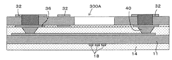
(2) つぎに、前記(A)で製造したフレキシブル基板100Aとリジッド基板200Aとを積層し、180℃、40kg/cm2で加熱プレスし(図3(b)参照)、半田バンプ40によって接続されたフレックスリジッド配線板300Aを得た(図9参照)。
(2) Next, the
フレキシブル基板の屈曲部周辺に、各開口面積が40000μm2、開口面積の総和:パターン残部面積=9:10であるような矩形の開口を有する格子状のダミーパターン18を形成した以外は、実施例1と同様にして、フレックスリジッド配線板300Aを製造した。
Example except that a lattice-
フレキシブル基板の屈曲部周辺に、各開口面積が90000μm2、開口面積の総和:パターン残部面積=11:10であるような矩形の開口を有する格子状のダミーパターン18を形成した以外は、実施例1と同様にして、フレックスリジッド配線板300Aを製造した。
Example except that a lattice-
フレキシブル基板の屈曲部周辺に、各開口面積が90000μm2、開口面積の総和:パターン残部面積=1:9であるような矩形の開口を有する格子状のダミーパターン18を形成した以外は、実施例1と同様にして、フレックスリジッド配線板300Aを製造した。
Example except that a lattice-
フレキシブル基板の屈曲部周辺に、各開口面積が90000μm2、開口面積の総和:パターン残部面積=2:8であるような矩形の開口を有する格子状のダミーパターン18を形成した以外は、実施例1と同様にして、フレックスリジッド配線板300Aを製造した。
Example except that a lattice-
フレキシブル基板の屈曲部周辺に、各開口面積が90000μm2、開口面積の総和:パターン残部面積=8:2であるような矩形の開口を有する格子状のダミーパターン18を形成した以外は、実施例1と同様にして、フレックスリジッド配線板300Aを製造した。
Example except that a lattice-
フレキシブル基板の屈曲部周辺に、各開口面積が90000μm2、開口面積の総和:パターン残部面積=9:1であるような矩形の開口を有する格子状のダミーパターン18を形成した以外は、実施例1と同様にして、フレックスリジッド配線板300Aを製造した。
Example except that a grid-
フレキシブル基板の屈曲部周辺に、各開口面積が7850μm2、開口面積の総和:パターン残部面積=10:10であるような円形の開口を有するダミーパターン18を形成した以外は、実施例1と同様にして、フレックスリジッド配線板300Aを製造した。
Except for forming a
フレキシブル基板の屈曲部周辺に、各開口面積が49087μm2、開口面積の総和:パターン残部面積=10:9であるような円形の開口を有するダミーパターン18を形成した以外は、実施例1と同様にして、フレックスリジッド配線板300Aを製造した。
Except for forming a
フレキシブル基板の屈曲部周辺に、各開口面積が125600μm2、開口面積の総和:パターン残部面積=11:10であるような円形の開口を有するダミーパターン18を形成した以外は、実施例1と同様にして、フレックスリジッド配線板300Aを製造した。
Except for forming a
フレキシブル基板の屈曲部周辺に、各開口面積が125600μm2、開口面積の総和:パターン残部面積=1:9であるような円形の開口を有する格子状のダミーパターン18を形成した以外は、実施例1と同様にして、フレックスリジッド配線板300Aを製造した。
Example except that a lattice-
フレキシブル基板の屈曲部周辺に、各開口面積が125600μm2、開口面積の総和:パターン残部面積=2:8であるような円形の開口を有する格子状のダミーパターン18を形成した以外は、実施例1と同様にして、フレックスリジッド配線板300Aを製造した。
Example except that a lattice-
フレキシブル基板の屈曲部周辺に、各開口面積が125600μm2、開口面積の総和:パターン残部面積=8:2であるような円形の開口を有する格子状のダミーパターン18を形成した以外は、実施例1と同様にして、フレックスリジッド配線板300Aを製造した。
Example except that a lattice-
フレキシブル基板の屈曲部周辺に、各開口面積が125600μm2、開口面積の総和:パターン残部面積=9:1であるような円形の開口を有する格子状のダミーパターン18を形成した以外は、実施例1と同様にして、フレックスリジッド配線板300Aを製造した。
Example except that a grid-
フレキシブル基板の屈曲部周辺に、各開口面積が10025μm2、開口面積の総和:パターン残部面積=10:10であるような、角部がアール形状をなす開口を有するダミーパターン18を形成した以外は、実施例1と同様にして、フレックスリジッド配線板300Aを製造した。
Except for forming a
フレキシブル基板の屈曲部周辺に、各開口面積が40090μm2、開口面積の総和:パターン残部面積=9:10であるような、角部がアール形状をなす開口を有するダミーパターン18を形成した以外は、実施例1と同様にして、フレックスリジッド配線板300Aを製造した。
Except for forming a
フレキシブル基板の屈曲部周辺に、各開口面積が90123μm2、開口面積の総和:パターン残部面積=11:10であるような、角部がアール形状をなす開口を有するダミーパターン18を形成した以外は、実施例1と同様にして、フレックスリジッド配線板300Aを製造した。
Except for forming a
フレキシブル基板の屈曲部周辺に、各開口面積が90123μm2、開口面積の総和:パターン残部面積=1:9であるような角部がアール形状をなす開口を有する格子状のダミーパターン18を形成した以外は、実施例1と同様にして、フレックスリジッド配線板300Aを製造した。
Around the bent portion of the flexible substrate, a grid-
フレキシブル基板の屈曲部周辺に、各開口面積が90123μm2、開口面積の総和:パターン残部面積=2:8であるような角部がアール形状をなす開口を有する格子状のダミーパターン18を形成した以外は、実施例1と同様にして、フレックスリジッド配線板300Aを製造した。
Around the bent portion of the flexible substrate, a grid-
フレキシブル基板の屈曲部周辺に、各開口面積が90123μm2、開口面積の総和:パターン残部面積=8:2であるような角部がアール形状をなす開口を有する格子状のダミーパターン18を形成した以外は、実施例1と同様にして、フレックスリジッド配線板300Aを製造した。
Around the bent portion of the flexible substrate, a lattice-
フレキシブル基板の屈曲部周辺に、各開口面積が90123μm2、開口面積の総和:パターン残部面積=9:1であるような角部がアール形状をなす開口を有する格子状のダミーパターン18を形成した以外は、実施例1と同様にして、フレックスリジッド配線板300Aを製造した。
Around the bent portion of the flexible substrate, a lattice-
フレキシブル基板の屈曲部周辺に、各開口面積が49087μm2、開口面積の総和:パターン残部面積=10:10であるような円形開口が千鳥状に配列されてなるダミーパターン18を形成した以外は、実施例1と同様にして、フレックスリジッド配線板300Aを製造した。
Except for forming a
フレキシブル基板の屈曲部周辺に、各開口面積が49087μm2、開口面積の総和:パターン残部面積=1:9であるような円形開口が千鳥状に配列されてなるダミーパターン18を形成した以外は、実施例1と同様にして、フレックスリジッド配線板300Aを製造した。
Except for forming a
フレキシブル基板の屈曲部周辺に、各開口面積が49087μm2、開口面積の総和:パターン残部面積=9:1であるような円形開口が千鳥状に配列されてなるダミーパターン18を形成した以外は、実施例1と同様にして、フレックスリジッド配線板300Aを製造した。
Except for forming a
フレキシブル基板の屈曲部周辺に、開口面積が49087μm2である円形開口と、開口面積が10000μm2である円形開口とが交互に配列され、それらの開口面積の総和:パターン残部面積=10:10であるような円形開口を有するダミーパターン18を形成した以外は、実施例1と同様にして、フレックスリジッド配線板300Aを製造した。
Around the bent portion of the flexible substrate, and the circular aperture opening area is 49087Myuemu 2, open area and a circular opening is 10000 2 are alternately arranged, the sum of their opening areas: pattern balance area = 10: 10 A flex-
フレキシブル基板の屈曲部周辺に、開口面積が49087μm2である円形開口と、開口面積が10000μm2である円形開口とが交互に配列され、それらの開口面積の総和:パターン残部面積=1:9であるような円形開口を有するダミーパターン18を形成した以外は、実施例1と同様にして、フレックスリジッド配線板300Aを製造した。
Around the bent portion of the flexible substrate, and the circular aperture opening area is 49087Myuemu 2, open area and a circular opening is 10000 2 are alternately arranged, the sum of their opening areas: pattern balance area = 1: 9 A flex-
フレキシブル基板の屈曲部周辺に、開口面積が49087μm2である円形開口と、開口面積が10000μm2である円形開口とが交互に配列され、それらの開口面積の総和:パターン残部面積=9:1であるような円形開口を有するダミーパターン18を形成した以外は、実施例1と同様にして、フレックスリジッド配線板300Aを製造した。
Around the bent portion of the flexible substrate, and the circular aperture opening area is 49087Myuemu 2, open area and a circular opening is 10000 2 are alternately arranged, the sum of their opening areas: pattern balance area = 9: 1 A flex-
フレキシブル基板の屈曲部周辺に、開口を有しないベタパターン(15mm×15mm)を形成した以外は、実施例1と同様にして、フレックスリジッド配線板300Aを製造した。
A flex-
ダミーパターンを形成しなかったこと以外は、実施例1と同様にして、フレックスリジッド配線板を製造した。 A flex-rigid wiring board was manufactured in the same manner as in Example 1 except that no dummy pattern was formed.
屈曲部周辺に、断面形状が矩形で、線幅が150μmである線状のダミーパターンを、隣接するパターン間の距離を30μmとして6本形成した以外は、実施例1と同様にして、フレックスリジッド配線板300Aを製造した。
In the same manner as in Example 1, except that six linear dummy patterns having a rectangular cross-sectional shape and a line width of 150 μm were formed around the bent portion with a distance between adjacent patterns of 30 μm. A
屈曲部周辺に、断面形状が矩形で、線幅が200μmである線状のダミーパターンを、隣接するパターン間の距離を150μmとして6本形成した以外は、実施例1と同様にして、フレックスリジッド配線板300Aを製造した。
In the same manner as in Example 1, except that six linear dummy patterns having a rectangular cross-sectional shape and a line width of 200 μm were formed around the bent portion with a distance between adjacent patterns of 150 μm. A
屈曲部周辺に、断面形状が矩形で、線幅が200μmである線状のダミーパターンを、隣接するパターン間の距離を100μmとして6本形成した以外は、実施例1と同様にして、フレックスリジッド配線板300Aを製造した。
In the same manner as in Example 1, except that six linear dummy patterns having a rectangular cross-sectional shape and a line width of 200 μm were formed around the bent portion with a distance between adjacent patterns of 100 μm. A
屈曲部周辺に、断面形状が裾角度75°の台形で、線幅が150μmである線状のダミーパターンを、隣接するパターン間の距離を300μmとして6本形成した以外は、実施例1と同様にして、フレックスリジッド配線板300Aを製造した。
Example 6 except that six linear dummy patterns having a trapezoidal cross-sectional shape with a skirt angle of 75 ° and a line width of 150 μm were formed around the bent portion with a distance between adjacent patterns of 300 μm. Thus, a flex-
屈曲部周辺に、断面形状が裾角度60°の台形で、線幅が250μmである線状のダミーパターンを、隣接するパターン間の距離を50μmとして6本形成した以外は、実施例1と同様にして、フレックスリジッド配線板300Aを製造した。
Example 6 except that six linear dummy patterns having a trapezoidal cross-sectional shape with a skirt angle of 60 ° and a line width of 250 μm were formed around the bent portion with a distance between adjacent patterns of 50 μm. Thus, a flex-
屈曲部周辺に、断面形状が裾角度45°の台形で、線幅が250μmである線状のダミーパターンを、隣接するパターン間の距離を50μmとして6本形成した以外は、実施例1と同様にして、フレックスリジッド配線板300Aを製造した。
Example 6 except that six linear dummy patterns with a cross-sectional shape of a trapezoid having a skirt angle of 45 ° and a line width of 250 μm were formed around the bent portion with a distance between adjacent patterns of 50 μm. Thus, a flex-
屈曲部周辺に、断面形状が矩形で、線幅が150μmである線状のダミーパターンを、隣接するパターン間の距離を300μmとして6本形成した以外は、実施例1と同様にして、フレックスリジッド配線板300Aを製造した。
In the same manner as in Example 1, except that six linear dummy patterns having a rectangular cross-sectional shape and a line width of 150 μm were formed around the bent portion with a distance between adjacent patterns of 300 μm. A
屈曲部周辺に、断面形状が裾角度75°の台形で、線幅が150μmである線状のダミーパターンを、隣接するパターン間の距離を300μmとして6本形成した以外は、実施例1と同様にして、フレックスリジッド配線板300Aを製造した。
Example 6 except that six linear dummy patterns having a trapezoidal cross-sectional shape with a skirt angle of 75 ° and a line width of 150 μm were formed around the bent portion with a distance between adjacent patterns of 300 μm. Thus, a flex-
フレキシブル基板を作製する出発材料として、厚さ20μmのガラスクロス(ガラス繊維の太さ平均1.5μm)にエポキシ系樹脂を含浸、乾燥させてなる絶縁性基材11の両面に、厚さが18μmの銅箔12を加熱プレスして、エポキシ系樹脂を硬化させてなる、厚さ50μmの両面銅張積層板を用い、屈曲部周辺に、断面形状が矩形で、線幅が100μmである線状のダミーパターンを、隣接するパターン間の距離を40μmとして6本形成した以外は、実施例1と同様にして、フレックスリジッド配線板300Aを製造した。
As a starting material for producing a flexible substrate, a glass cloth having a thickness of 20 μm (average thickness of glass fiber 1.5 μm) is impregnated with an epoxy resin and dried on both surfaces of an insulating
フレキシブル基板を作製する出発材料として、厚さ20μmのガラスクロス(ガラス繊維の太さ平均3.0μm)にエポキシ系樹脂を含浸、乾燥させてなる絶縁性基材11の両面に、厚さが18μmの銅箔12を加熱プレスして、エポキシ系樹脂を硬化させてなる厚さ50μmの両面銅張積層板を用い、屈曲部周辺に、断面形状が矩形で、線幅が100μmである線状のダミーパターンを、隣接するパターン間の距離を40μmとして6本形成した以外は、実施例1と同様にして、フレックスリジッド配線板300Aを製造した。
As a starting material for producing a flexible substrate, a glass cloth having a thickness of 20 μm (average thickness of glass fiber: 3.0 μm) is impregnated with an epoxy resin and dried on both surfaces of an insulating
フレキシブル基板を作製する出発材料として、厚さ20μmのガラスクロス(ガラス繊維の太さ平均4.0μm)にエポキシ系樹脂を含浸、乾燥させてなる絶縁性基材11の両面に、厚さが18μmの銅箔12を加熱プレスして、エポキシ系樹脂を硬化させてなる、厚さ50μmの両面銅張積層板を用い、屈曲部周辺に、断面形状が矩形で、線幅が100μmである線状のダミーパターンを、隣接するパターン間の距離を40μmとして6本形成した以外は、実施例1と同様にして、フレックスリジッド配線板300Aを製造した。
As a starting material for producing a flexible substrate, a glass cloth having a thickness of 20 μm (average thickness of glass fiber: 4.0 μm) is impregnated with an epoxy resin and dried on both sides of an insulating
フレキシブル基板を作製する出発材料として、厚さ30μmのガラスクロス(ガラス繊維の太さ平均5.0μm)にエポキシ系樹脂を含浸、乾燥させてなる絶縁性基材11の両面に、厚さが18μmの銅箔12を加熱プレスして、エポキシ系樹脂を硬化させてなる厚さ60μmの両面銅張積層板を用い、屈曲部周辺に、断面形状が矩形で、線幅が100μmである線状のダミーパターンを、隣接するパターン間の距離を40μmとして6本形成した以外は、実施例1と同様にして、フレックスリジッド配線板300Aを製造した。
As a starting material for producing a flexible substrate, a glass cloth having a thickness of 30 μm (average thickness of glass fiber: 5.0 μm on average) is impregnated with an epoxy resin and dried on both sides of an insulating
フレキシブル基板を作製する出発材料として、厚さ60μmのガラスクロス(ガラス繊維の太さ平均5.0μm)にエポキシ系樹脂を含浸、乾燥させてなる絶縁性基材11の両面に、厚さが18μmの銅箔12を加熱プレスして、エポキシ系樹脂を硬化させてなる厚さ100μmの両面銅張積層板を用い、屈曲部周辺に、断面形状が矩形で、線幅が100μmである線状のダミーパターンを、隣接するパターン間の距離を40μmとして6本形成した以外は、実施例1と同様にして、フレックスリジッド配線板300Aを製造した。
As a starting material for producing a flexible substrate, a glass cloth having a thickness of 60 μm (average thickness of glass fiber: 5.0 μm on average) is impregnated with an epoxy resin and dried on both surfaces of an insulating
フレキシブル基板を作製する出発材料として、厚さ20μmのガラスクロス(ガラス繊維の太さ平均1.5μm)にエポキシ系樹脂を含浸、乾燥させてなる絶縁性基材11の両面に、厚さが18μmの銅箔12を加熱プレスして、エポキシ系樹脂を硬化させてなる厚さ50μmの両面銅張積層板を用い、屈曲部周辺に、断面形状が裾角度70°の台形で、線幅が100μmである線状のダミーパターンを、隣接するパターン間の距離を40μmとして6本形成した以外は、実施例1と同様にして、フレックスリジッド配線板300Aを製造した。
As a starting material for producing a flexible substrate, a glass cloth having a thickness of 20 μm (average thickness of glass fiber 1.5 μm) is impregnated with an epoxy resin and dried on both surfaces of an insulating
フレキシブル基板を作製する出発材料として、厚さ20μmのガラスクロス(ガラス繊維の太さ平均3.0μm)にエポキシ系樹脂を含浸、乾燥させてなる絶縁性基材11の両面に、厚さが18μmの銅箔12を加熱プレスして、エポキシ系樹脂を硬化させてなる厚さ50μmの両面銅張積層板を用い、屈曲部周辺に、断面形状が裾角度70°の台形で、線幅が100μmである線状のダミーパターンを、隣接するパターン間の距離を40μmとして6本形成した以外は、実施例1と同様にして、フレックスリジッド配線板300Aを製造した。
As a starting material for producing a flexible substrate, a glass cloth having a thickness of 20 μm (average thickness of glass fiber: 3.0 μm) is impregnated with an epoxy resin and dried on both surfaces of an insulating
フレキシブル基板を作製する出発材料として、厚さ20μmのガラスクロス(ガラス繊維の太さ平均4.0μm)にエポキシ系樹脂を含浸、乾燥させてなる絶縁性基材11の両面に、厚さが18μmの銅箔12を加熱プレスして、エポキシ系樹脂を硬化させてなる厚さ50μmの両面銅張積層板を用い、屈曲部周辺に、断面形状が裾角度70°の台形で、線幅が100μmである線状のダミーパターンを、隣接するパターン間の距離を40μmとして6本形成した以外は、実施例1と同様にして、フレックスリジッド配線板300Aを製造した。
As a starting material for producing a flexible substrate, a glass cloth having a thickness of 20 μm (average thickness of glass fiber: 4.0 μm) is impregnated with an epoxy resin and dried on both sides of an insulating
フレキシブル基板を作製する出発材料として、厚さ30μmのガラスクロス(ガラス繊維の太さ平均5.0μm)にエポキシ系樹脂を含浸、乾燥させてなる絶縁性基材11の両面に、厚さが18μmの銅箔12を加熱プレスして、エポキシ系樹脂を硬化させてなる厚さ60μmの両面銅張積層板を用い、屈曲部周辺に、断面形状が裾角度70°の台形で、線幅が100μmである線状のダミーパターンを、隣接するパターン間の距離を40μmとして6本形成した以外は、実施例1と同様にして、フレックスリジッド配線板300Aを製造した。
As a starting material for producing a flexible substrate, a glass cloth having a thickness of 30 μm (average thickness of glass fiber: 5.0 μm on average) is impregnated with an epoxy resin and dried on both sides of an insulating
フレキシブル基板を作製する出発材料として、厚さ60μmのガラスクロス(ガラス繊維の太さ平均5.0μm)にエポキシ系樹脂を含浸、乾燥させてなる絶縁性基材11の両面に、厚さが18μmの銅箔12を加熱プレスして、エポキシ系樹脂を硬化させてなる厚さ100μmの両面銅張積層板を用い、屈曲部周辺に、断面形状が裾角度70°の台形で、線幅が100μmである線状のダミーパターンを、隣接するパターン間の距離を40μmとして6本形成した以外は、実施例1と同様にして、フレックスリジッド配線板300Aを製造した。
As a starting material for producing a flexible substrate, a glass cloth having a thickness of 60 μm (average thickness of glass fiber: 5.0 μm on average) is impregnated with an epoxy resin and dried on both surfaces of an insulating
フレキシブル基板を作製する出発材料として、厚さ15μmのガラスクロス(ガラス繊維の太さ平均4.0μm)にエポキシ系樹脂を含浸、乾燥させてなる絶縁性基材11の両面に、厚さが18μmの銅箔12を加熱プレスして、エポキシ系樹脂を硬化させてなる厚さ50μmの両面銅張積層板を用い、屈曲部周辺に、断面形状が矩形で、線幅が100μmである線状のダミーパターンを、隣接するパターン間の距離を40μmとして6本形成した以外は、実施例1と同様にして、フレックスリジッド配線板300Aを製造した。
As a starting material for producing a flexible substrate, a glass cloth having a thickness of 15 μm (average thickness of glass fiber: 4.0 μm) is impregnated with an epoxy resin and dried on both surfaces of an insulating
フレキシブル基板を作製する出発材料として、厚さ100μmのガラスクロス(ガラス繊維の太さ平均7.0μm)にエポキシ系樹脂を含浸、乾燥させてなる絶縁性基材11の両面に、厚さが18μmの銅箔12を加熱プレスして、エポキシ系樹脂を硬化させてなる厚さ150μmの両面銅張積層板を用い、屈曲部周辺に、断面形状が矩形で、線幅が100μmである線状のダミーパターンを、隣接するパターン間の距離を40μmとして6本形成した以外は、実施例1と同様にして、フレックスリジッド配線板300Aを製造した。
As a starting material for producing a flexible substrate, a glass cloth having a thickness of 100 μm (average thickness of glass fiber: 7.0 μm) is impregnated with an epoxy resin and dried on both sides of an insulating
フレキシブル基板を作製する出発材料として、厚さ15μmのガラスクロス(ガラス繊維の太さ平均4.0μm)にエポキシ系樹脂を含浸、乾燥させてなる絶縁性基材11の両面に、厚さが18μmの銅箔12を加熱プレスして、エポキシ系樹脂を硬化させてなる厚さ50μmの両面銅張積層板を用い、屈曲部周辺に、断面形状が裾角度70°の台形で、線幅が100μmである線状のダミーパターンを、隣接するパターン間の距離を40μmとして6本形成した以外は、実施例1と同様にして、フレックスリジッド配線板300Aを製造した。
As a starting material for producing a flexible substrate, a glass cloth having a thickness of 15 μm (average thickness of glass fiber: 4.0 μm) is impregnated with an epoxy resin and dried on both surfaces of an insulating
フレキシブル基板を作製する出発材料として、厚さ100μmのガラスクロス(ガラス繊維の太さ平均7.0μm)にエポキシ系樹脂を含浸、乾燥させてなる絶縁性基材11の両面に、厚さが18μmの銅箔12を加熱プレスして、エポキシ系樹脂を硬化させてなる厚さ150μmの両面銅張積層板を用い、屈曲部周辺に、断面形状が裾角度70°の台形で、線幅が100μmである線状のダミーパターンを、隣接するパターン間の距離を40μmとして6本形成した以外は、実施例1と同様にして、フレックスリジッド配線板300Aを製造した。
As a starting material for producing a flexible substrate, a glass cloth having a thickness of 100 μm (average thickness of glass fiber: 7.0 μm) is impregnated with an epoxy resin and dried on both sides of an insulating
(1) 本発明にかかるフレックスリジッド配線板を製造するに当たって、それを構成するフレキシブル基板100Bを作製する出発材料として、厚さ20μm(厚さが30μm以下)のガラスクロス(ガラス繊維の太さ平均4.0μm)にエポキシ系樹脂を含浸、乾燥させてなる絶縁性基材52の両面に、厚さが18μmの銅箔がラミネートされた厚さ50μmである両面銅張積層板(日立化成:製品名「E−67」)を用いた。
(1) In manufacturing a flex-rigid wiring board according to the present invention, a glass cloth (average thickness of glass fibers) having a thickness of 20 μm (thickness of 30 μm or less) is used as a starting material for producing a flexible substrate 100B constituting the flexible rigid wiring board. Double-sided copper-clad laminate with a thickness of 50 μm obtained by laminating a copper foil with a thickness of 18 μm on both sides of an insulating
(2) まず、厚さ0.05mmの両面銅張積層板の両面にドライフィルムレジストをラミネートし、露光、現像によりエッチングレジストを形成した後、塩化第二銅水溶液を用いたエッチング処理によって、一方の表面には、線幅が300μmである導体回路の配線パターン54を形成し、その配線パターン形成面と反対側の表面には、屈曲部周辺に、格子状のダミーパターン56(開口形状が矩形、各開口面積が10000μm2、開口面積の総和:パターン残部面積=10:10)を形成した(図10(a)参照)。
(2) First, a dry film resist was laminated on both sides of a 0.05 mm thick double-sided copper-clad laminate, and after forming an etching resist by exposure and development, one of the two was etched by using an aqueous cupric chloride solution. A conductive
(3) 上記(2)により配線パターン54およびダミーパターン56を形成した基板の両面に、スクリーン印刷によってソルダーレジスト(日本ポリテック製:NPR-90)を塗布し、400mj/cm2の条件下で露光し、150℃、1時間の条件下で乾燥させることによって、カバー層58を形成した(図10(b)参照)。
(3) Solder resist (NPR-90 made by Nippon Polytech Co., Ltd.) was applied by screen printing on both sides of the substrate on which the
(4) 上記カバー層58を形成した基板の両面に対して、屈曲が必要な箇所を開口(符号62で示す)したプリプレグ60(松下電工製:R-1661)と、厚さ12μmの銅箔64とを積層し(図10(c)参照)、その積層体を圧力35kg/cm2 、温度180℃で加熱プレスした(図10(d)参照)。
(4) A prepreg 60 (made by Matsushita Electric Co., Ltd .: R-1661) having an opening (indicated by reference numeral 62) where a portion that needs to be bent is formed on both surfaces of the substrate on which the
(5) 上記(4)で得た積層体の表面に、所定の照射条件にて炭酸ガスレーザ照射を行って、銅箔64に直径100μmの開口66を形成すると共に、その開口66から更に照射条件を変えた炭酸ガスレーザ照射を行って、基板を貫通する直径300μmの貫通孔68を形成した(図10(e)参照)。
レーザ照射の後、過マンガン酸溶液を用いて、貫通孔68内に残存する樹脂残さ(スミア)を除去するためにデスミア処理を行なった。
(5) The surface of the laminate obtained in (4) above is irradiated with a carbon dioxide laser under predetermined irradiation conditions to form an
After the laser irradiation, desmear treatment was performed using a permanganic acid solution to remove the resin residue (smear) remaining in the through hole 68.
(6) 上記(5)で形成した貫通孔68の内壁にPd触媒を付与し、以下のような組成および条件のもとで無電解銅めっき処理を施した後、さらに電解銅めっき処理を施すことによって、貫通孔68の内壁を含んだ基板全体に銅めっき層70を形成した(図10(f)参照)。
これによって、めっきスルーホール76が形成された。
(6) A Pd catalyst is applied to the inner wall of the through hole 68 formed in the above (5), electroless copper plating is performed under the following composition and conditions, and further electrolytic copper plating is performed. Thus, the
As a result, a plated through
(無電解銅めっき溶液)
硫酸銅 10g/リトッル
HCHO 8g/リットル
NaOH 5g/リットル
ロッシェル塩 45g/リットル
温度 30℃
(Electroless copper plating solution)
Copper sulfate 10g / Little HCHO 8g / liter NaOH 5g / liter Rochelle salt 45g / liter Temperature 30 ° C
(電解銅めっき溶液)
硫酸 180g/リットル
硫酸銅 80g/リットル
アトテックジャパン製 商品名 カパラシドGL
1ml/リットル
(めっき条件)
電流密度 2A/dm2
時間 30分
温度 25℃
(Electrolytic copper plating solution)
Sulfuric acid 180g / liter Copper sulfate 80g / liter Atotech Japan product name Kaparaside GL
1 ml / liter (plating conditions)
Current density 2A / dm 2
Time 30 minutes Temperature 25 ° C
(7) 次いで、上記(6)にて銅めっき層70を形成した基板の表面および裏面にドライフィルムレジストをラミネートし、露光、現像によりエッチングレジストを形成した後、塩化第二銅水溶液を用いたエッチング処理を施して、基板の表面および裏面にそれぞれ配線パターン72、74を形成した。
前記配線パターン72および74は、めっきスルーホール76を介してフレキシブル基板52上に形成された配線パターン54に電気的に接続される(図10(g)参照)。
(7) Next, a dry film resist was laminated on the front and back surfaces of the substrate on which the
The
(8)さらに、ソルダーレジスト層を形成した後、ルーターにて外形加工を行って、表面に配線パターン54が有し、裏面にダミーパターン56を有するフレックスリジッド配線板300Bを製造した。
(8) Further, after forming a solder resist layer, the outer shape was processed by a router to manufacture a flex-rigid wiring board 300B having the
フレキシブル基板の屈曲部周辺に、各開口面積が40000μm2、開口面積の総和:パターン残部面積=9:10であるような矩形の開口を有する格子状のダミーパターン56を形成した以外は、実施例45と同様にして、フレックスリジッド配線板300Bを製造した。
Example except that a lattice-
フレキシブル基板の屈曲部周辺に、各開口面積が90000μm2、開口面積の総和:パターン残部面積=11:10であるような矩形の開口を有する格子状のダミーパターン56を形成した以外は、実施例45と同様にして、フレックスリジッド配線板300Bを製造した。
Example except that a lattice-
フレキシブル基板の屈曲部周辺に、各開口面積が90000μm2、開口面積の総和:パターン残部面積=1:9であるような矩形の開口を有する格子状のダミーパターン18を形成した以外は、実施例45と同様にして、フレックスリジッド配線板300Bを製造した。
Example except that a lattice-
フレキシブル基板の屈曲部周辺に、各開口面積が90000μm2、開口面積の総和:パターン残部面積=2:8であるような矩形の開口を有する格子状のダミーパターン18を形成した以外は、実施例45と同様にして、フレックスリジッド配線板300Bを製造した。
Example except that a lattice-
フレキシブル基板の屈曲部周辺に、各開口面積が90000μm2、開口面積の総和:パターン残部面積=8:2であるような矩形の開口を有する格子状のダミーパターン18を形成した以外は、実施例45と同様にして、フレックスリジッド配線板300Bを製造した。
Example except that a lattice-
フレキシブル基板の屈曲部周辺に、各開口面積が90000μm2、開口面積の総和:パターン残部面積=9:1であるような矩形の開口を有する格子状のダミーパターン18を形成した以外は、実施例45と同様にして、フレックスリジッド配線板300Bを製造した。
Example except that a grid-
フレキシブル基板の屈曲部周辺に、各開口面積が7850μm2、開口面積の総和:パターン残部面積=10:10であるような円形の開口を有するダミーパターン56を形成した以外は、実施例45と同様にして、フレックスリジッド配線板300Bを製造した。
Example 45 is similar to Example 45 except that a
フレキシブル基板の屈曲部周辺に、各開口面積が49087μm2、開口面積の総和:パターン残部面積=9:10であるような円形の開口を有するダミーパターン56を形成した以外は、実施例45と同様にして、フレックスリジッド配線板300Bを製造した。
Similar to Example 45, except that a
フレキシブル基板の屈曲部周辺に、各開口面積が125600μm2、開口面積の総和:パターン残部面積=11:10であるような円形の開口を有するダミーパターン56を形成した以外は、実施例45と同様にして、フレックスリジッド配線板300Bを製造した。
Example 45 is the same as in Example 45 except that a
フレキシブル基板の屈曲部周辺に、各開口面積が125600μm2、開口面積の総和:パターン残部面積=1:9であるような円形の開口を有する格子状のダミーパターン18を形成した以外は、実施例45と同様にして、フレックスリジッド配線板300Bを製造した。
Example except that a lattice-
フレキシブル基板の屈曲部周辺に、各開口面積が125600μm2、開口面積の総和:パターン残部面積=2:8であるような円形の開口を有する格子状のダミーパターン18を形成した以外は、実施例45と同様にして、フレックスリジッド配線板300Bを製造した。
Example except that a lattice-
フレキシブル基板の屈曲部周辺に、各開口面積が125600μm2、開口面積の総和:パターン残部面積=8:2であるような円形の開口を有する格子状のダミーパターン18を形成した以外は、実施例45と同様にして、フレックスリジッド配線板300Bを製造した。
Example except that a lattice-
フレキシブル基板の屈曲部周辺に、各開口面積が125600μm2、開口面積の総和:パターン残部面積=9:1であるような円形の開口を有する格子状のダミーパターン18を形成した以外は、実施例45と同様にして、フレックスリジッド配線板300Bを製造した。
Example except that a grid-
フレキシブル基板の屈曲部周辺に、各開口面積が10025μm2、開口面積の総和:パターン残部面積=10:10であるような、角部がアール形状をなす開口を有するダミーパターン56を形成した以外は、実施例45と同様にして、フレックスリジッド配線板300Bを製造した。
Except for forming a
フレキシブル基板の屈曲部周辺に、各開口面積が40090μm2、開口面積の総和:パターン残部面積=9:10であるような、角部がアール形状をなす開口を有するダミーパターン56を形成した以外は、実施例45と同様にして、フレックスリジッド配線板300Bを製造した。
Except for forming a
フレキシブル基板の屈曲部周辺に、各開口面積が90123μm2、開口面積の総和:パターン残部面積=11:10であるような、角部がアール形状をなす開口を有するダミーパターン56を形成した以外は、実施例45と同様にして、フレックスリジッド配線板300Bを製造した。
Except for forming a
フレキシブル基板の屈曲部周辺に、各開口面積が90123μm2、開口面積の総和:パターン残部面積=1:9であるような角部がアール形状をなす開口を有する格子状のダミーパターン18を形成した以外は、実施例45と同様にして、フレックスリジッド配線板300Bを製造した。
Around the bent portion of the flexible substrate, a grid-
フレキシブル基板の屈曲部周辺に、各開口面積が90123μm2、開口面積の総和:パターン残部面積=2:8であるような角部がアール形状をなす開口を有する格子状のダミーパターン18を形成した以外は、実施例45と同様にして、フレックスリジッド配線板300Bを製造した。
Around the bent portion of the flexible substrate, a grid-
フレキシブル基板の屈曲部周辺に、各開口面積が90123μm2、開口面積の総和:パターン残部面積=8:2であるような角部がアール形状をなす開口を有する格子状のダミーパターン18を形成した以外は、実施例45と同様にして、フレックスリジッド配線板300Bを製造した。
Around the bent portion of the flexible substrate, a lattice-
フレキシブル基板の屈曲部周辺に、各開口面積が90123μm2、開口面積の総和:パターン残部面積=9:1であるような角部がアール形状をなす開口を有する格子状のダミーパターン18を形成した以外は、実施例45と同様にして、フレックスリジッド配線板300Bを製造した。
Around the bent portion of the flexible substrate, a lattice-
フレキシブル基板の屈曲部周辺に、各開口面積が49087μm2、開口面積の総和:パターン残部面積=10:10であるような円形開口が千鳥状に配列されてなるダミーパターン56を形成した以外は、実施例45と同様にして、フレックスリジッド配線板300Bを製造した。
Except for forming a
フレキシブル基板の屈曲部周辺に、各開口面積が49087μm2、開口面積の総和:パターン残部面積=1:9であるような円形開口が千鳥状に配列されてなるダミーパターン18を形成した以外は、実施例45と同様にして、フレックスリジッド配線板300Bを製造した。
Except for forming a
フレキシブル基板の屈曲部周辺に、各開口面積が49087μm2、開口面積の総和:パターン残部面積=9:1であるような円形開口が千鳥状に配列されてなるダミーパターン18を形成した以外は、実施例45と同様にして、フレックスリジッド配線板300Bを製造した。
Except for forming a
フレキシブル基板の屈曲部周辺に、開口面積が49087μm2である円形開口と、開口面積が10000μm2である円形開口とが交互に配列され、それらの開口面積の総和:パターン残部面積=10:10であるような円形開口を有するダミーパターン56を形成した以外は、実施例45と同様にして、フレックスリジッド配線板300Bを製造した。
Around the bent portion of the flexible substrate, and the circular aperture opening area is 49087Myuemu 2, open area and a circular opening is 10000 2 are alternately arranged, the sum of their opening areas: pattern balance area = 10: 10 A flex-rigid wiring board 300B was manufactured in the same manner as in Example 45 except that a
フレキシブル基板の屈曲部周辺に、開口面積が49087μm2である円形開口と、開口面積が10000μm2である円形開口とが交互に配列され、それらの開口面積の総和:パターン残部面積=1:9であるような円形開口を有するダミーパターン18を形成した以外は、実施例45と同様にして、フレックスリジッド配線板300Bを製造した。
Around the bent portion of the flexible substrate, and the circular aperture opening area is 49087Myuemu 2, open area and a circular opening is 10000 2 are alternately arranged, the sum of their opening areas: pattern balance area = 1: 9 A flex-rigid wiring board 300B was manufactured in the same manner as in Example 45 except that the
フレキシブル基板の屈曲部周辺に、開口面積が49087μm2である円形開口と、開口面積が10000μm2である円形開口とが交互に配列され、それらの開口面積の総和:パターン残部面積=9:1であるような円形開口を有するダミーパターン18を形成した以外は、実施例45と同様にして、フレックスリジッド配線板300Bを製造した。
Around the bent portion of the flexible substrate, and the circular aperture opening area is 49087Myuemu 2, open area and a circular opening is 10000 2 are alternately arranged, the sum of their opening areas: pattern balance area = 9: 1 A flex-rigid wiring board 300B was manufactured in the same manner as in Example 45 except that the
フレキシブル基板の屈曲部周辺に、開口を有しないベタパターン(15mm×15mm)を形成した以外は、実施例45と同様にして、フレックスリジッド配線板300Bを製造した。 A flex-rigid wiring board 300B was manufactured in the same manner as in Example 45 except that a solid pattern (15 mm × 15 mm) having no opening was formed around the bent portion of the flexible substrate.
ダミーパターンを形成しなかったこと以外は、実施例45と同様にして、フレックスリジッド配線板を製造した。 A flex-rigid wiring board was manufactured in the same manner as in Example 45 except that no dummy pattern was formed.
屈曲部周辺に、断面形状が矩形で、線幅が150μmである線状のダミーパターンを、隣接するパターン間の距離を30μmとして6本形成した以外は、実施例45と同様にして、フレックスリジッド配線板300Bを製造した。 In the same manner as in Example 45, except that six linear dummy patterns having a rectangular cross-sectional shape and a line width of 150 μm were formed around the bent portion with a distance between adjacent patterns of 30 μm, flex rigid A wiring board 300B was manufactured.
屈曲部周辺に、断面形状が矩形で、線幅が200μmである線状のダミーパターンを、隣接するパターン間の距離を150μmとして6本形成した以外は、実施例45と同様にして、フレックスリジッド配線板300Bを製造した。 In the same manner as in Example 45, except that six linear dummy patterns having a rectangular cross-sectional shape and a line width of 200 μm were formed around the bent portion with a distance between adjacent patterns of 150 μm, flex rigid A wiring board 300B was manufactured.
屈曲部周辺に、断面形状が矩形で、線幅が200μmである線状のダミーパターンを、隣接するパターン間の距離を100μmとして6本形成した以外は、実施例45と同様にして、フレックスリジッド配線板300Bを製造した。 In the same manner as in Example 45, except that six linear dummy patterns having a rectangular cross-sectional shape and a line width of 200 μm were formed around the bent portion with a distance between adjacent patterns of 100 μm, flex rigid A wiring board 300B was manufactured.
屈曲部周辺に、断面形状が裾角度75°の台形で、線幅が150μmである線状のダミーパターンを、隣接するパターン間の距離を300μmとして6本形成した以外は、実施例45と同様にして、フレックスリジッド配線板300Bを製造した。 Example 45, except that six linear dummy patterns having a trapezoidal cross-sectional shape with a skirt angle of 75 ° and a line width of 150 μm were formed around the bent portion with a distance between adjacent patterns of 300 μm. Thus, a flex-rigid wiring board 300B was manufactured.
屈曲部周辺に、断面形状が裾角度60°の台形で、線幅が250μmである線状のダミーパターンを、隣接するパターン間の距離を50μmとして6本形成した以外は、実施例45と同様にして、フレックスリジッド配線板300Bを製造した。 Similar to Example 45, except that six linear dummy patterns having a trapezoidal cross-sectional shape with a skirt angle of 60 ° and a line width of 250 μm were formed around the bent portion with a distance between adjacent patterns of 50 μm. Thus, a flex-rigid wiring board 300B was manufactured.
屈曲部周辺に、断面形状が裾角度45°の台形で、線幅が250μmである線状のダミーパターンを、隣接するパターン間の距離を50μmとして6本形成した以外は、実施例45と同様にして、フレックスリジッド配線板300Bを製造した。 Similar to Example 45 except that six linear dummy patterns having a trapezoidal cross-sectional shape with a skirt angle of 45 ° and a line width of 250 μm were formed around the bent portion with a distance between adjacent patterns of 50 μm. Thus, a flex-rigid wiring board 300B was manufactured.
屈曲部周辺に、断面形状が矩形で、線幅が150μmである線状のダミーパターンを、隣接するパターン間の距離を300μmとして6本形成した以外は、実施例45と同様にして、フレックスリジッド配線板300Bを製造した。 In the same manner as in Example 45, except that six linear dummy patterns having a rectangular cross-sectional shape and a line width of 150 μm were formed around the bent portion with a distance between adjacent patterns of 300 μm, flex rigid A wiring board 300B was manufactured.
屈曲部周辺に、断面形状が裾角度75°の台形で、線幅が150μmである線状のダミーパターンを、隣接するパターン間の距離を300μmとして6本形成した以外は、実施例45と同様にして、フレックスリジッド配線板300Bを製造した。 Example 45, except that six linear dummy patterns having a trapezoidal cross-sectional shape with a skirt angle of 75 ° and a line width of 150 μm were formed around the bent portion with a distance between adjacent patterns of 300 μm. Thus, a flex-rigid wiring board 300B was manufactured.
フレキシブル基板を作製する出発材料として、厚さ20μmのガラスクロス(ガラス繊維の太さ平均1.5μm)にエポキシ系樹脂を含浸、乾燥させてなる絶縁性基材11の両面に、厚さが18μmの銅箔12を加熱プレスして、エポキシ系樹脂を硬化させてなる、厚さ50μmの両面銅張積層板を用い、屈曲部周辺に、断面形状が矩形で、線幅が100μmである線状のダミーパターンを、隣接するパターン間の距離を40μmとして6本形成した以外は、実施例45と同様にして、フレックスリジッド配線板300Bを製造した。
As a starting material for producing a flexible substrate, a glass cloth having a thickness of 20 μm (average thickness of glass fiber 1.5 μm) is impregnated with an epoxy resin and dried on both surfaces of an insulating
フレキシブル基板を作製する出発材料として、厚さ20μmのガラスクロス(ガラス繊維の太さ平均3.0μm)にエポキシ系樹脂を含浸、乾燥させてなる絶縁性基材11の両面に、厚さが18μmの銅箔12を加熱プレスして、エポキシ系樹脂を硬化させてなる厚さ50μmの両面銅張積層板を用い、屈曲部周辺に、断面形状が矩形で、線幅が100μmである線状のダミーパターンを、隣接するパターン間の距離を40μmとして6本形成した以外は、実施例45と同様にして、フレックスリジッド配線板300Bを製造した。
As a starting material for producing a flexible substrate, a glass cloth having a thickness of 20 μm (average thickness of glass fiber: 3.0 μm) is impregnated with an epoxy resin and dried on both surfaces of an insulating
フレキシブル基板を作製する出発材料として、厚さ20μmのガラスクロス(ガラス繊維の太さ平均4.0μm)にエポキシ系樹脂を含浸、乾燥させてなる絶縁性基材52の両面に、厚さが18μmの銅箔を加熱プレスして、エポキシ系樹脂を硬化させてなる厚さ50μmの両面銅張積層板を用い、屈曲部周辺に、断面形状が矩形で、線幅が100μmである線状のダミーパターンを、隣接するパターン間の距離を40μmとして6本形成した以外は、実施例45と同様にして、フレックスリジッド配線板300Bを製造した。
As a starting material for producing a flexible substrate, a glass cloth having a thickness of 20 μm (average thickness of glass fiber: 4.0 μm) is impregnated with an epoxy resin and dried on both sides of an insulating
フレキシブル基板を作製する出発材料として、厚さ30μmのガラスクロス(ガラス繊維の太さ平均5.0μm)にエポキシ系樹脂を含浸、乾燥させてなる絶縁性基材52の両面に、厚さが18μmの銅箔を加熱プレスして、エポキシ系樹脂を硬化させてなる厚さ60μmの両面銅張積層板を用い、屈曲部周辺に、断面形状が矩形で、線幅が100μmである線状のダミーパターンを、隣接するパターン間の距離を40μmとして6本形成した以外は、実施例45と同様にして、フレックスリジッド配線板300Bを製造した。
As a starting material for producing a flexible substrate, a glass cloth having a thickness of 30 μm (average thickness of glass fiber: 5.0 μm) is impregnated with an epoxy resin and dried on both surfaces of an insulating
フレキシブル基板を作製する出発材料として、厚さ60μmのガラスクロス(ガラス繊維の太さ平均5.0μm)にエポキシ系樹脂を含浸、乾燥させてなる絶縁性基材52の両面に、厚さが18μmの銅箔を加熱プレスして、エポキシ系樹脂を硬化させてなる厚さ100μmの両面銅張積層板を用い、屈曲部周辺に、断面形状が矩形で、線幅が100μmである線状のダミーパターンを、隣接するパターン間の距離を40μmとして6本形成した以外は、実施例45と同様にして、フレックスリジッド配線板300Bを製造した。
As a starting material for producing a flexible substrate, a glass cloth having a thickness of 60 μm (average thickness of glass fiber: 5.0 μm) is impregnated with an epoxy resin and dried on both sides of an insulating
フレキシブル基板を作製する出発材料として、厚さ20μmのガラスクロス(ガラス繊維の太さ平均1.5μm)にエポキシ系樹脂を含浸、乾燥させてなる絶縁性基材11の両面に、厚さが18μmの銅箔12を加熱プレスして、エポキシ系樹脂を硬化させてなる厚さ50μmの両面銅張積層板を用い、屈曲部周辺に、断面形状が裾角度70°の台形で、線幅が100μmである線状のダミーパターンを、隣接するパターン間の距離を40μmとして6本形成した以外は、実施例45と同様にして、フレックスリジッド配線板300Bを製造した。
As a starting material for producing a flexible substrate, a glass cloth having a thickness of 20 μm (average thickness of glass fiber 1.5 μm) is impregnated with an epoxy resin and dried on both surfaces of an insulating
フレキシブル基板を作製する出発材料として、厚さ20μmのガラスクロス(ガラス繊維の太さ平均3.0μm)にエポキシ系樹脂を含浸、乾燥させてなる絶縁性基材11の両面に、厚さが18μmの銅箔12を加熱プレスして、エポキシ系樹脂を硬化させてなる厚さ50μmの両面銅張積層板を用い、屈曲部周辺に、断面形状が裾角度70°の台形で、線幅が100μmである線状のダミーパターンを、隣接するパターン間の距離を40μmとして6本形成した以外は、実施例45と同様にして、フレックスリジッド配線板300Bを製造した。
As a starting material for producing a flexible substrate, a glass cloth having a thickness of 20 μm (average thickness of glass fiber: 3.0 μm) is impregnated with an epoxy resin and dried on both surfaces of an insulating
フレキシブル基板を作製する出発材料として、厚さ20μmのガラスクロス(ガラス繊維の太さ平均4.0μm)にエポキシ系樹脂を含浸、乾燥させてなる絶縁性基材52の両面に、厚さが18μmの銅箔を加熱プレスして、エポキシ系樹脂を硬化させてなる厚さ50μmの両面銅張積層板を用い、屈曲部周辺に、断面形状が裾角度70°の台形で、線幅が100μmである線状のダミーパターンを、隣接するパターン間の距離を40μmとして6本形成した以外は、実施例45と同様にして、フレックスリジッド配線板300Bを製造した。
As a starting material for producing a flexible substrate, a glass cloth having a thickness of 20 μm (average thickness of glass fiber: 4.0 μm) is impregnated with an epoxy resin and dried on both surfaces of an insulating
フレキシブル基板を作製する出発材料として、厚さ30μmのガラスクロス(ガラス繊維の太さ平均5.0μm)にエポキシ系樹脂を含浸、乾燥させてなる絶縁性基材52の両面に、厚さが18μmの銅箔を加熱プレスして、エポキシ系樹脂を硬化させてなる厚さ60μmの両面銅張積層板を用い、屈曲部周辺に、断面形状が裾角度70°の台形で、線幅が100μmである線状のダミーパターンを、隣接するパターン間の距離を40μmとして6本形成した以外は、実施例45と同様にして、フレックスリジッド配線板300Bを製造した。
As a starting material for producing a flexible substrate, a glass cloth having a thickness of 30 μm (average thickness of glass fiber: 5.0 μm) is impregnated with an epoxy resin and dried on both surfaces of an insulating
フレキシブル基板を作製する出発材料として、厚さ60μmのガラスクロス(ガラス繊維の太さ平均5.0μm)にエポキシ系樹脂を含浸、乾燥させてなる絶縁性基材52の両面に、厚さが18μmの銅箔を加熱プレスして、エポキシ系樹脂を硬化させてなる厚さ100μmの両面銅張積層板を用い、屈曲部周辺に、断面形状が裾角度70°の台形で、線幅が100μmである線状のダミーパターンを、隣接するパターン間の距離を40μmとして6本形成した以外は、実施例45と同様にして、フレックスリジッド配線板300Bを製造した。
As a starting material for producing a flexible substrate, a glass cloth having a thickness of 60 μm (average thickness of glass fiber: 5.0 μm) is impregnated with an epoxy resin and dried on both sides of an insulating
フレキシブル基板を作製する出発材料として、厚さ15μmのガラスクロス(ガラス繊維の太さ平均4.0μm)にエポキシ系樹脂を含浸、乾燥させてなる絶縁性基材52の両面に、厚さが18μmの銅箔を加熱プレスして、エポキシ系樹脂を硬化させてなる厚さ50μmの両面銅張積層板を用い、屈曲部周辺に、断面形状が矩形で、線幅が100μmである線状のダミーパターンを、隣接するパターン間の距離を40μmとして6本形成した以外は、実施例45と同様にして、フレックスリジッド配線板300Bを製造した。
As a starting material for producing a flexible substrate, a glass cloth having a thickness of 15 μm (average thickness of glass fiber: 4.0 μm) is impregnated with an epoxy resin and dried on both sides of an insulating
フレキシブル基板を作製する出発材料として、厚さ100μmのガラスクロス(ガラス繊維の太さ平均7.0μm)にエポキシ系樹脂を含浸、乾燥させてなる絶縁性基材52の両面に、厚さが18μmの銅箔を加熱プレスして、エポキシ系樹脂を硬化させてなる厚さ150μmの両面銅張積層板を用い、屈曲部周辺に、断面形状が矩形で、線幅が100μmである線状のダミーパターンを、隣接するパターン間の距離を40μmとして6本形成した以外は、実施例45と同様にして、フレックスリジッド配線板300Bを製造した。
As a starting material for producing a flexible substrate, a glass cloth having a thickness of 100 μm (average thickness of glass fiber: 7.0 μm) is impregnated with an epoxy resin and dried on both sides of an insulating
フレキシブル基板を作製する出発材料として、厚さ15μmのガラスクロス(ガラス繊維の太さ平均4.0μm)にエポキシ系樹脂を含浸、乾燥させてなる絶縁性基材52の両面に、厚さが18μmの銅箔を加熱プレスして、エポキシ系樹脂を硬化させてなる厚さ50μmの両面銅張積層板を用い、屈曲部周辺に、断面形状が裾角度70°の台形で、線幅が100μmである線状のダミーパターンを、隣接するパターン間の距離を40μmとして6本形成した以外は、実施例45と同様にして、フレックスリジッド配線板300Bを製造した。
As a starting material for producing a flexible substrate, a glass cloth having a thickness of 15 μm (average thickness of glass fiber: 4.0 μm) is impregnated with an epoxy resin and dried on both sides of an insulating
フレキシブル基板を作製する出発材料として、厚さ100μmのガラスクロス(ガラス繊維の太さ平均7.0μm)にエポキシ系樹脂を含浸、乾燥させてなる絶縁性基材52の両面に、厚さが18μmの銅箔を加熱プレスして、エポキシ系樹脂を硬化させてなる厚さ150μmの両面銅張積層板を用い、屈曲部周辺に、断面形状が裾角度70°の台形で、線幅が100μmである線状のダミーパターンを、隣接するパターン間の距離を40μmとして6本形成した以外は、実施例45と同様にして、フレックスリジッド配線板300Bを製造した。
As a starting material for producing a flexible substrate, a glass cloth having a thickness of 100 μm (average thickness of glass fiber: 7.0 μm) is impregnated with an epoxy resin and dried on both sides of an insulating
以上説明したように、フレキシブル基板とリジッド基板との電気的接続が塊状導電体を介して行われる形態の実施例1〜44、参考例1〜6、比較例1およびフレキシブル基板とリジッド基板との電気的接続がめっきスルーホールを介して行われる形態の実施例45〜88、参考例7〜12、比較例2について、それぞれ以下の(1)および(2)のような評価試験を行った。 As described above, Examples 1-44, Reference Examples 1-6, Comparative Example 1 and Examples of the embodiment in which the electrical connection between the flexible substrate and the rigid substrate is performed via the bulk conductor are made between the flexible substrate and the rigid substrate. The following evaluation tests (1) and (2) were performed on Examples 45 to 88, Reference Examples 7 to 12, and Comparative Example 2 in a form in which electrical connection was made through plated through holes.
(1)導通試験
フレキシブル基板の折り曲げを3回繰り返した後に、フレキシブル基板の導体回路の配線パターンの電気的導通の有無を調べた。それらの導通試験の結果を、表1〜3および表4〜6に示す。
なお、電気的導通が有れば○とし、無ければ×とした。
(1) Conduction test After repeating the bending of the flexible substrate three times, the presence or absence of electrical continuity in the wiring pattern of the conductor circuit of the flexible substrate was examined. The results of those continuity tests are shown in Tables 1 to 3 and Tables 4 to 6.
In addition, it was set to ○ when there was electrical continuity, and × when there was no electrical conduction.
(2)信頼性(耐折性)評価試験
JIS C5016に準拠するMIT testを実施した。この試験は、フレキシブル基板の折り曲げを繰り返し行い、フレキシブル基板の導体回路の配線パターンが断線するまでの回数を測定したもので、それらの試験結果を、表1〜3および表4〜6に示す。
なお、断線までの折り曲げ回数が50以上である場合には、◎とし、30以上である場合には、○とし、29以下である場合には、△とし、15以下の場合には、×とした。
(2) Reliability (folding resistance) evaluation test
MIT test compliant with JIS C5016 was conducted. In this test, the flexible substrate was repeatedly bent and the number of times until the wiring pattern of the conductor circuit of the flexible substrate was disconnected was measured. The test results are shown in Tables 1 to 3 and Tables 4 to 6.
In addition, when the number of times of bending until breakage is 50 or more, ◎, when it is 30 or more, ○, when it is 29 or less, △, when it is 15 or less, × did.
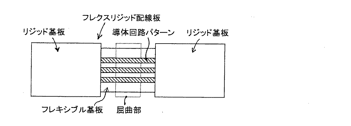
以上の試験結果から、実施例1〜28(実施例45〜72)については、開口総面積/パターン面積が1/9〜9/1であるような格子状のダミーパターンが、電気的接続性および屈曲性(耐折性)に優れており、特に、開口パターンが円形で開口総面積/パターン面積が11/10であるようなダミーパターンや、大小の円形からなる組合せパターンからなり、開口総面積/パターン面積が10/10であるようなダミーパターンが優れていることがわかる。 From the above test results, in Examples 1 to 28 (Examples 45 to 72), a lattice-like dummy pattern having a total opening area / pattern area of 1/9 to 9/1 is electrically connected. In addition, it is excellent in flexibility (folding resistance), and is composed of a dummy pattern having a circular opening pattern and a total opening area / pattern area of 11/10, or a combination pattern consisting of large and small circles. It can be seen that a dummy pattern having an area / pattern area of 10/10 is excellent.
また、実施例29〜34(実施例73〜78)および参考例1,2(参考例7、8)については、線幅が150〜250μm、線間距離が30μm以上である線状のダミーパターンが、電気的接続性および屈曲性(耐折性)に優れており、特に、線幅が200μm以上、線間距離が100μm以下であるようなダミーパターンがより優れており、さらに、線幅が200μm、線間距離が50μmであるようなダミーパターンが最も優れていることがわかった。 For Examples 29 to 34 (Examples 73 to 78) and Reference Examples 1 and 2 (Reference Examples 7 and 8), a linear dummy pattern having a line width of 150 to 250 μm and a distance between lines of 30 μm or more. However, it has excellent electrical connectivity and flexibility (folding resistance), and in particular, a dummy pattern having a line width of 200 μm or more and a distance between lines of 100 μm or less is more excellent. It was found that a dummy pattern having a thickness of 200 μm and a line-to-line distance of 50 μm was most excellent.
また、線状のダミーパターンの断面形状が台形である場合には、その裾角度が45°以上であるダミーパターンが、電気的接続性および屈曲性(耐折性)に優れ、特に、裾角度75°であるようなパターンが最も優れていることがわかった。 In addition, when the cross-sectional shape of the linear dummy pattern is trapezoidal, the dummy pattern whose skirt angle is 45 ° or more is excellent in electrical connectivity and bendability (folding resistance). It was found that the pattern having the angle of 75 ° is the most excellent.
さらに、実施例35〜44(実施例79〜88)および参考例3〜6(参考例9〜12)は、フレキシブル基板の絶縁性基材の厚さが、100μm以下であり、ガラスクロスの厚さが30μm以下であるようなフレキシブル基板にダミーパターンを設けた場合に、電気的接続性および屈曲性(耐折性)に優れており、特に、絶縁性基材の厚さが50μmであり、ガラスクロスの厚さが20μmであるようなフレキシブル基板に設けたダミーパターンが最も優れていることがわかった。 Further, in Examples 35 to 44 (Examples 79 to 88) and Reference Examples 3 to 6 (Reference Examples 9 to 12), the thickness of the insulating substrate of the flexible substrate is 100 μm or less, and the thickness of the glass cloth When a dummy pattern is provided on a flexible substrate having a thickness of 30 μm or less, it has excellent electrical connectivity and bendability (folding resistance). In particular, the thickness of the insulating substrate is 50 μm, It turned out that the dummy pattern provided in the flexible substrate whose glass cloth thickness is 20 micrometers is the most excellent.
また、上記各実施例1〜88および参考例1〜12にかかるフレックスリジッド配線板は、フレキシブル基板の屈曲部における屈曲具合が、曲率半径で表すとき、0.1〜0.25mmの範囲内であり、ダミーパターンを形成しない比較例1(曲率半径:0.05mm)にかかるフレックスリジッド配線板に比して、大幅にその屈曲具合を大きくすることができることがわかる。 Moreover, the flex-rigid wiring boards according to the above Examples 1 to 88 and Reference Examples 1 to 12 are within the range of 0.1 to 0.25 mm when the bending state of the bent portion of the flexible substrate is expressed by the radius of curvature. It can be seen that the degree of bending can be greatly increased as compared with the flex-rigid wiring board according to comparative example 1 (curvature radius: 0.05 mm) in which no dummy pattern is formed.
以上のように、本発明にかかるフレックスリジッド配線板は、折りたたみ式の携帯電話等の携帯用電子機器に好適に用いられる。 As described above, the flex-rigid wiring board according to the present invention is suitably used for portable electronic devices such as a folding mobile phone.
11 絶縁性基材(ガラスクロス+樹脂)
12 銅箔
13 導体回路の配線パターン
14 カバー層
15 開口
16 接続用電極パッド
18 ダミーパターン
21 絶縁性基材
22 銅箔
24、26 開口
28 銅めっき層
32、34 導体回路の配線パターン
36 接続用電極パッド
40 コーン形状突起(半田バンプ)
52 絶縁性基材
54 導体回路の配線パターン
56 ダミーパターン
58 カバー層
60 プリプレグ
64 銅箔
66 貫通孔
70 銅めっき層
72、74 導体回路の配線パターン
76 めっきスルーホール
100A フレキシブル基板
200A リジッド基板
300A フレックスリジッド配線板
300B フレックスリジッド配線板
11 Insulating substrate (glass cloth + resin)
12
52 Insulating
Claims (14)
前記フレキシブル基板の絶縁性基材は、ガラスクロスに樹脂を含浸、乾燥させてなる屈曲可能な基材であり、
前記フレキシブル基板の一方の表面には導体回路を形成し、他方の表面には、屈曲部付近にダミーパターンを形成したことを特徴とするフレックスリジッド配線板。 Connects a rigid rigid board with a conductor circuit on an insulating substrate and a flexible flexible board with a conductor circuit on an insulating base material and a cover lay to cover the conductor circuit. In the flex-rigid circuit board
The insulating base material of the flexible substrate is a base material that can be bent by impregnating and drying a glass cloth with a resin,
A flex-rigid wiring board, wherein a conductor circuit is formed on one surface of the flexible substrate, and a dummy pattern is formed near a bent portion on the other surface.
The flex-rigid wiring board according to claim 1, wherein the dummy pattern is formed on a surface that becomes an inner side when the flexible substrate is bent.
Priority Applications (1)
| Application Number | Priority Date | Filing Date | Title |
|---|---|---|---|
| JP2004109237A JP4437051B2 (en) | 2004-04-01 | 2004-04-01 | Flex rigid wiring board |
Applications Claiming Priority (1)
| Application Number | Priority Date | Filing Date | Title |
|---|---|---|---|
| JP2004109237A JP4437051B2 (en) | 2004-04-01 | 2004-04-01 | Flex rigid wiring board |
Publications (2)
| Publication Number | Publication Date |
|---|---|
| JP2005294639A true JP2005294639A (en) | 2005-10-20 |
| JP4437051B2 JP4437051B2 (en) | 2010-03-24 |
Family
ID=35327212
Family Applications (1)
| Application Number | Title | Priority Date | Filing Date |
|---|---|---|---|
| JP2004109237A Expired - Fee Related JP4437051B2 (en) | 2004-04-01 | 2004-04-01 | Flex rigid wiring board |
Country Status (1)
| Country | Link |
|---|---|
| JP (1) | JP4437051B2 (en) |
Cited By (11)
| Publication number | Priority date | Publication date | Assignee | Title |
|---|---|---|---|---|
| JP2007123735A (en) * | 2005-10-31 | 2007-05-17 | Kyocera Chemical Corp | Method of manufacturing base material for wiring board and laminated base material for wiring board, and wiring board |
| JP2007324236A (en) * | 2006-05-30 | 2007-12-13 | Nof Corp | Resin composition used for printed wiring board film and use thereof |
| WO2008087851A1 (en) * | 2007-01-19 | 2008-07-24 | Sharp Kabushiki Kaisha | Flexible substrate and semiconductor device |
| JP2012015322A (en) * | 2010-06-30 | 2012-01-19 | Toshiba Corp | Electronic apparatus |
| US8344486B2 (en) | 2008-07-16 | 2013-01-01 | Sharp Kabushiki Kaisha | Semiconductor device and display apparatus |
| JP2015138876A (en) * | 2014-01-22 | 2015-07-30 | 株式会社デンソー | flexible circuit board |
| JP2018063383A (en) * | 2016-10-14 | 2018-04-19 | 株式会社ジャパンディスプレイ | Display device and method for manufacturing display device |
| WO2018212089A1 (en) * | 2017-05-18 | 2018-11-22 | シャープ株式会社 | Method for manufacturing display module and method for inspecting display module |
| KR20190045693A (en) * | 2017-10-24 | 2019-05-03 | 삼성전자주식회사 | Printed circuit board and semiconductor package including the same |
| JP2020013904A (en) * | 2018-07-18 | 2020-01-23 | キオクシア株式会社 | Semiconductor storage device |
| JP2023111743A (en) * | 2022-01-31 | 2023-08-10 | 富士電機株式会社 | Wiring board, power converter |
Citations (7)
| Publication number | Priority date | Publication date | Assignee | Title |
|---|---|---|---|---|
| JPS593567U (en) * | 1982-06-29 | 1984-01-11 | 松下電器産業株式会社 | Double-sided flexible printed circuit board |
| JPS60124056U (en) * | 1984-01-31 | 1985-08-21 | パイオニア株式会社 | flexible printed circuit board |
| JPH03109368U (en) * | 1990-02-23 | 1991-11-11 | ||
| JPH0541171U (en) * | 1991-11-06 | 1993-06-01 | オリンパス光学工業株式会社 | Flexible printed circuit board |
| JPH06314862A (en) * | 1993-04-28 | 1994-11-08 | Nitto Denko Corp | Flexible circuit board |
| JPH07106728A (en) * | 1993-10-04 | 1995-04-21 | Mitsui Toatsu Chem Inc | Rigid flex printed wiring board and manufacturing method thereof |
| JPH07183663A (en) * | 1993-12-24 | 1995-07-21 | Mitsubishi Gas Chem Co Inc | Rigid flexible multilayer printed board |
-
2004
- 2004-04-01 JP JP2004109237A patent/JP4437051B2/en not_active Expired - Fee Related
Patent Citations (7)
| Publication number | Priority date | Publication date | Assignee | Title |
|---|---|---|---|---|
| JPS593567U (en) * | 1982-06-29 | 1984-01-11 | 松下電器産業株式会社 | Double-sided flexible printed circuit board |
| JPS60124056U (en) * | 1984-01-31 | 1985-08-21 | パイオニア株式会社 | flexible printed circuit board |
| JPH03109368U (en) * | 1990-02-23 | 1991-11-11 | ||
| JPH0541171U (en) * | 1991-11-06 | 1993-06-01 | オリンパス光学工業株式会社 | Flexible printed circuit board |
| JPH06314862A (en) * | 1993-04-28 | 1994-11-08 | Nitto Denko Corp | Flexible circuit board |
| JPH07106728A (en) * | 1993-10-04 | 1995-04-21 | Mitsui Toatsu Chem Inc | Rigid flex printed wiring board and manufacturing method thereof |
| JPH07183663A (en) * | 1993-12-24 | 1995-07-21 | Mitsubishi Gas Chem Co Inc | Rigid flexible multilayer printed board |
Cited By (18)
| Publication number | Priority date | Publication date | Assignee | Title |
|---|---|---|---|---|
| JP2007123735A (en) * | 2005-10-31 | 2007-05-17 | Kyocera Chemical Corp | Method of manufacturing base material for wiring board and laminated base material for wiring board, and wiring board |
| JP2007324236A (en) * | 2006-05-30 | 2007-12-13 | Nof Corp | Resin composition used for printed wiring board film and use thereof |
| WO2008087851A1 (en) * | 2007-01-19 | 2008-07-24 | Sharp Kabushiki Kaisha | Flexible substrate and semiconductor device |
| JP2008177402A (en) * | 2007-01-19 | 2008-07-31 | Sharp Corp | Flexible substrate and semiconductor device |
| TWI396266B (en) * | 2008-07-16 | 2013-05-11 | 夏普股份有限公司 | Semiconductor device and display device |
| US8344486B2 (en) | 2008-07-16 | 2013-01-01 | Sharp Kabushiki Kaisha | Semiconductor device and display apparatus |
| KR101234461B1 (en) * | 2008-07-16 | 2013-02-18 | 샤프 가부시키가이샤 | Semiconductor device and display device |
| US8593820B2 (en) | 2010-06-30 | 2013-11-26 | Kabushiki Kaisha Toshiba | Flexible printed wiring board and electronic apparatus |
| JP2012015322A (en) * | 2010-06-30 | 2012-01-19 | Toshiba Corp | Electronic apparatus |
| JP2015138876A (en) * | 2014-01-22 | 2015-07-30 | 株式会社デンソー | flexible circuit board |
| JP2018063383A (en) * | 2016-10-14 | 2018-04-19 | 株式会社ジャパンディスプレイ | Display device and method for manufacturing display device |
| WO2018212089A1 (en) * | 2017-05-18 | 2018-11-22 | シャープ株式会社 | Method for manufacturing display module and method for inspecting display module |
| KR20190045693A (en) * | 2017-10-24 | 2019-05-03 | 삼성전자주식회사 | Printed circuit board and semiconductor package including the same |
| KR102437245B1 (en) | 2017-10-24 | 2022-08-30 | 삼성전자주식회사 | Printed circuit board and semiconductor package including the same |
| JP2020013904A (en) * | 2018-07-18 | 2020-01-23 | キオクシア株式会社 | Semiconductor storage device |
| JP7141877B2 (en) | 2018-07-18 | 2022-09-26 | キオクシア株式会社 | semiconductor storage device |
| JP2023111743A (en) * | 2022-01-31 | 2023-08-10 | 富士電機株式会社 | Wiring board, power converter |
| JP7844897B2 (en) | 2022-01-31 | 2026-04-14 | 富士電機株式会社 | Wiring boards, power converters |
Also Published As
| Publication number | Publication date |
|---|---|
| JP4437051B2 (en) | 2010-03-24 |
Similar Documents
| Publication | Publication Date | Title |
|---|---|---|
| JP4536430B2 (en) | Flex rigid wiring board | |
| KR100987619B1 (en) | Multilayer printed wiring board | |
| KR100865060B1 (en) | Rigid-flex wiring board | |
| JP5006035B2 (en) | Flex rigid wiring board and manufacturing method thereof | |
| KR19990006770A (en) | Manufacturing method of composite wiring board, flexible board, semiconductor device and composite wiring board | |
| KR20070070224A (en) | Multilayer printed wiring board | |
| JP4437051B2 (en) | Flex rigid wiring board | |
| TW200412205A (en) | Double-sided printed circuit board without via holes and method of fabricating the same | |
| CN101406112A (en) | Circuit board and connection substrate | |
| CN101959376A (en) | The manufacture method of multilayer flexible printed wiring plate and multilayer circuit basis material | |
| JP2015038908A (en) | Flex-rigid wiring board | |
| KR20070073730A (en) | Wiring boards, wiring materials and manufacturing method of copper clad laminate and wiring board | |
| JP2013030811A (en) | Display element module using multilayer flexible printed wiring board | |
| KR20070017577A (en) | Flex Rigid Wiring Boards and Manufacturing Method Thereof | |
| CN223080204U (en) | Printed circuit boards and electronic devices | |
| KR101231522B1 (en) | The printed circuit board and the method for manufacturing the same | |
| JP2005109188A (en) | Circuit board and multilayer board, and method for manufacturing circuit board and multilayer board | |
| KR101776299B1 (en) | Printed circuit board using bump structure and Manufacturing method of the same | |
| JP2009043917A (en) | Multilayer wiring board and manufacturing method thereof | |
| JP2004111758A (en) | Multilayer flexible wiring board and its production method | |
| JP2015038907A (en) | Flex-rigid wiring board | |
| JP2005353861A (en) | Flex rigid wiring board | |
| JP2003124585A (en) | Universal printed circuit board | |
| JPH06164145A (en) | Multilayer interconnection board |
Legal Events
| Date | Code | Title | Description |
|---|---|---|---|
| A621 | Written request for application examination |
Free format text: JAPANESE INTERMEDIATE CODE: A621 Effective date: 20070319 |
|
| A977 | Report on retrieval |
Free format text: JAPANESE INTERMEDIATE CODE: A971007 Effective date: 20090430 |
|
| A131 | Notification of reasons for refusal |
Free format text: JAPANESE INTERMEDIATE CODE: A131 Effective date: 20090609 |
|
| A521 | Written amendment |
Free format text: JAPANESE INTERMEDIATE CODE: A523 Effective date: 20090807 |
|
| TRDD | Decision of grant or rejection written | ||
| A01 | Written decision to grant a patent or to grant a registration (utility model) |
Free format text: JAPANESE INTERMEDIATE CODE: A01 Effective date: 20091215 |
|
| A01 | Written decision to grant a patent or to grant a registration (utility model) |
Free format text: JAPANESE INTERMEDIATE CODE: A01 |
|
| A61 | First payment of annual fees (during grant procedure) |
Free format text: JAPANESE INTERMEDIATE CODE: A61 Effective date: 20100104 |
|
| R150 | Certificate of patent or registration of utility model |
Free format text: JAPANESE INTERMEDIATE CODE: R150 |
|
| FPAY | Renewal fee payment (event date is renewal date of database) |
Free format text: PAYMENT UNTIL: 20130108 Year of fee payment: 3 |
|
| FPAY | Renewal fee payment (event date is renewal date of database) |
Free format text: PAYMENT UNTIL: 20130108 Year of fee payment: 3 |
|
| LAPS | Cancellation because of no payment of annual fees |