JP2005295542A - Linearity compensation circuit - Google Patents
Linearity compensation circuit Download PDFInfo
- Publication number
- JP2005295542A JP2005295542A JP2005083845A JP2005083845A JP2005295542A JP 2005295542 A JP2005295542 A JP 2005295542A JP 2005083845 A JP2005083845 A JP 2005083845A JP 2005083845 A JP2005083845 A JP 2005083845A JP 2005295542 A JP2005295542 A JP 2005295542A
- Authority
- JP
- Japan
- Prior art keywords
- harmonic
- input
- input signal
- signal
- corrected
- Prior art date
- Legal status (The legal status is an assumption and is not a legal conclusion. Google has not performed a legal analysis and makes no representation as to the accuracy of the status listed.)
- Granted
Links
Images

Classifications
-
- H—ELECTRICITY
- H03—ELECTRONIC CIRCUITRY
- H03M—CODING; DECODING; CODE CONVERSION IN GENERAL
- H03M1/00—Analogue/digital conversion; Digital/analogue conversion
- H03M1/06—Continuously compensating for, or preventing, undesired influence of physical parameters
- H03M1/0617—Continuously compensating for, or preventing, undesired influence of physical parameters characterised by the use of methods or means not specific to a particular type of detrimental influence
- H03M1/0626—Continuously compensating for, or preventing, undesired influence of physical parameters characterised by the use of methods or means not specific to a particular type of detrimental influence by filtering
-
- H—ELECTRICITY
- H03—ELECTRONIC CIRCUITRY
- H03M—CODING; DECODING; CODE CONVERSION IN GENERAL
- H03M1/00—Analogue/digital conversion; Digital/analogue conversion
- H03M1/06—Continuously compensating for, or preventing, undesired influence of physical parameters
- H03M1/0614—Continuously compensating for, or preventing, undesired influence of physical parameters of harmonic distortion
-
- H—ELECTRICITY
- H03—ELECTRONIC CIRCUITRY
- H03M—CODING; DECODING; CODE CONVERSION IN GENERAL
- H03M1/00—Analogue/digital conversion; Digital/analogue conversion
- H03M1/12—Analogue/digital converters
-
- H—ELECTRICITY
- H03—ELECTRONIC CIRCUITRY
- H03M—CODING; DECODING; CODE CONVERSION IN GENERAL
- H03M1/00—Analogue/digital conversion; Digital/analogue conversion
- H03M1/12—Analogue/digital converters
- H03M1/14—Conversion in steps with each step involving the same or a different conversion means and delivering more than one bit
- H03M1/16—Conversion in steps with each step involving the same or a different conversion means and delivering more than one bit with scale factor modification, i.e. by changing the amplification between the steps
- H03M1/164—Conversion in steps with each step involving the same or a different conversion means and delivering more than one bit with scale factor modification, i.e. by changing the amplification between the steps the steps being performed sequentially in series-connected stages
-
- H—ELECTRICITY
- H03—ELECTRONIC CIRCUITRY
- H03M—CODING; DECODING; CODE CONVERSION IN GENERAL
- H03M1/00—Analogue/digital conversion; Digital/analogue conversion
- H03M1/12—Analogue/digital converters
- H03M1/34—Analogue value compared with reference values
- H03M1/38—Analogue value compared with reference values sequentially only, e.g. successive approximation type
- H03M1/44—Sequential comparisons in series-connected stages with change in value of analogue signal
Landscapes
- Engineering & Computer Science (AREA)
- Theoretical Computer Science (AREA)
- Amplifiers (AREA)
- Filters And Equalizers (AREA)
Abstract
【課題】高調波歪の高調波をキャンセルする際に発生する低次の高調波もキャンセルできる直線性補償回路10を提供する。
【解決手段】高調波歪の補正されていない入力信号が高調波補正ユニット142〜14Mと、これら高調波補正ユニットの遅延時間と同じ補償遅延回路12に供給される。高調波補正ユニットの各々は、ヒルベルト変換フィルタを用いて個別に補正された高調波成分を発生する。加算器16は、補償遅延回路12と、高調波補正ユニット142〜14Mとの出力信号を加算して、高調波歪の高調波をキャンセルした補正済入力信号を発生する。
【選択図】図1
Provided is a linearity compensation circuit capable of canceling low-order harmonics generated when canceling harmonics of harmonic distortion.
An input signal whose harmonic distortion is not corrected is supplied to the harmonic correction units 14 2 to 14 M and a compensation delay circuit 12 having the same delay time as the harmonic correction units. Each of the harmonic correction units generates harmonic components that are individually corrected using a Hilbert transform filter. The adder 16 adds the output signals of the compensation delay circuit 12 and the harmonic correction units 14 2 to 14 M to generate a corrected input signal that cancels the harmonics of the harmonic distortion.
[Selection] Figure 1
Description
本発明は、一般に、直線性エラーの補正に関し、特に、アナログ・デジタル変換器(ADC)などの信号処理システムにおいて発生する高調波をキャンセルすることにより直線性を補償する回路に関する。 The present invention relates generally to linearity error correction, and more particularly to a circuit that compensates for linearity by canceling harmonics generated in a signal processing system such as an analog-to-digital converter (ADC).
総ての形式の非線形システム、即ち、以下に示すシステムS()により歪が発生する。
S(f(t)+g(t))≠S(f(t))+S(g(t))
なお、f(t)及びg(t)は2つの信号である。非線形システムの入力信号がある期間Tにわたって繰り返す場合、メモリのない非線形システムを通過する経路の信号も同じ期間にわたって繰り返される。フーリエ理論には、次の条件がある。
a)周期Tの総ての繰り返し信号は、直流オフセット、周期Tの基本正弦波、及び基本波の高調波の和により表すことができる。
b)基本波及び高調波の各々は、繰り返し信号の波形により独自に決まる振幅及び位相を有する。
正弦周波数は、その周期又はサイクル時間の逆数であるので、基本周波数は、1秒当たり1/Tサイクル、即ち、1/Tヘルツである。周期Tの正弦波の高調波は、基本周波数の整数倍の周波数であるので、n次高調波は、周波数がn/Tであり、周期がT/nである。
Distortion is generated by all types of non-linear systems, ie, the system S () shown below.
S (f (t) + g (t)) ≠ S (f (t)) + S (g (t))
Note that f (t) and g (t) are two signals. If the input signal of the nonlinear system repeats over a period T, the signal in the path through the nonlinear system without memory is also repeated over the same period. There are the following conditions in Fourier theory.
a) All repetitive signals of period T can be represented by the sum of DC offset, fundamental sine wave of period T, and harmonics of the fundamental wave.
b) Each of the fundamental wave and the harmonic wave has an amplitude and a phase that are uniquely determined by the waveform of the repetitive signal.
Since the sine frequency is the reciprocal of its period or cycle time, the fundamental frequency is 1 / T cycle per second,
数学的には、周波数fで繰り返す実信号Y(t)は、次のように表すことができる。
Y(t)=DC+Σn=1-M(A(n,f)sin(2πnft+P(n,f)))
A(n,f)は、基本周波数のn次高調波の振幅であり、P(n,f)は、対応する位相である。角周波数の単位はラジンアン/秒で2πf=ωであるので、1つの円、即ち、1サイクルは2πラジアンとなる。実現可能なシステムでは、高周波数の経路が制限されるので、高次高調波が制限される。例えば、アナログ・システムは、最大の駆動電流能力及び容量負荷により制限されるので、実際には、Mは、無限大にまで拡張されない。よって、繰り返し信号は、Tと、M個の振幅{A}及び位相{P}の有限の2組とにより決まる。
Mathematically, the real signal Y (t) repeated at the frequency f can be expressed as follows.
Y (t) = DC + Σ n = 1-M (A (n, f) sin (2πnft + P (n, f)))
A (n, f) is the amplitude of the nth harmonic of the fundamental frequency, and P (n, f) is the corresponding phase. Since the unit of the angular frequency is radians / second and 2πf = ω, one circle, that is, one cycle is 2π radians. In a feasible system, high frequency paths are limited, so high order harmonics are limited. For example, analog systems are limited by maximum drive current capability and capacitive loading, so in practice M is not extended to infinity. Thus, the repetitive signal is determined by T and two finite sets of M amplitudes {A} and phases {P}.
基本周波数を非線形システムの入力に供給すると、その出力は、基本波自体と、その種々の高調波とから成る。入力信号には高調波がないので、このシステム出力の各高調波の振幅は、基本波の振幅に関連し、その高調波歪の尺度となる。スプリアス・フリー・ダイナミック・レンジ(SFDR:Spurious Free Dynamic Range)は、純粋な正弦波入力周波数の所定範囲における基本波に対する最大高調波の相対的な大きさの尺度である。ADCは、ディザ信号が付加されるとき、特に複雑な入力に対して、通常、そのSFDRの尺度は、非常に良好である。 When the fundamental frequency is supplied to the input of the nonlinear system, its output consists of the fundamental itself and its various harmonics. Since the input signal has no harmonics, the amplitude of each harmonic of this system output is related to the fundamental amplitude and is a measure of its harmonic distortion. The spurious free dynamic range (SFDR) is a measure of the relative magnitude of the highest harmonic relative to the fundamental in a given range of pure sine wave input frequencies. An ADC usually has a very good measure of its SFDR, especially for complex inputs when a dither signal is added.
いくつかの非線形電子装置において、時間的に変化する入力に対して回路のどこかでその入力自体を変調して、出力に高調波を直接的に発生することが可能である。信号の自己変調の「フィンガープリント」は、非常に少ない識別可能な高調波を有する出力であり、通常、高調波の次数を非常に高速に認識できる。これは、n個の小さな信号の掛け算により各高調波nが生じるためであり、3次高調波でさえ目立たなくできるためである。例えば、アナログ・バッファやドライバの動作は、電源に影響を与え、次に、これがその後のアナログ信号電圧を変調する。多段のパイプライン形式のアナログ・デジタル変換器(ADC)において、各段の多入力フラッシュADCを駆動するのに強力なバッファが必要な場合もある。また、小さな異なる複数の信号を各段の間で増幅するので、高調波の数は、段の数に関連する。 In some non-linear electronic devices, it is possible to modulate a time-varying input somewhere in the circuit itself to generate harmonics directly at the output. The “fingerprint” of the signal's self-modulation is an output with very few identifiable harmonics and can usually recognize the harmonic order very quickly. This is because each harmonic n is generated by multiplication of n small signals, and even the third harmonic can be made inconspicuous. For example, the operation of an analog buffer or driver affects the power supply, which in turn modulates the subsequent analog signal voltage. In a multi-stage pipelined analog-to-digital converter (ADC), a powerful buffer may be required to drive the multi-input flash ADC of each stage. Also, since a number of different small signals are amplified between each stage, the number of harmonics is related to the number of stages.
いくつかの場合において、1個以上の経路で所定の高調波を発生するかもしれない。異なる経路が異なる遅延の場合、櫛形(comb)応答となるかもしれない。これは、量子化歪による歪よりも非常に小さいが、入力周波数に応じた高調波振幅の迅速な変化として現れるかもしれない。櫛形特性では、いくつかの高調波を無効にすることが非常に困難になるかもしれない。 In some cases, a given harmonic may be generated in one or more paths. If different paths have different delays, a comb response may result. This is much less than the distortion due to quantization distortion, but may appear as a rapid change in harmonic amplitude depending on the input frequency. Comb characteristics can make it very difficult to disable some harmonics.
自己変調高調波をキャンセルするために、信号自体の掛け算から成る加算エラー項を考察する。
Y(t)=X(t)+KX(t)2
ここで、Kは小さいと仮定する。エラー項を補正するには、次のようにする。
X'(t)≒Y(t)-K'Y(t)2
K'=Kの場合、上述の式をY(t)で置き換え、展開して簡略化すると、次のようになる。
X'(t)≒X(t)-2K2X(t)3-K3K(t)4
小さなKに対して、最後の2つの項は一層小さく、その近似が正確となる。他のパワーに対しても同様なとなる。
To cancel the self-modulating harmonics, consider an additive error term consisting of multiplication of the signal itself.
Y (t) = X (t) + KX (t) 2
Here, it is assumed that K is small. To correct the error term:
X '(t) ≒ Y (t) -K'Y (t) 2
When K ′ = K, the above equation is replaced with Y (t) and expanded to simplify it as follows.
X '(t) ≒ X (t) -2K 2 X (t) 3 -K 3 K (t) 4
For small K, the last two terms are smaller and the approximation is accurate. The same applies to other powers.
このメカニズムにより、大きな信号高調波を正確に補正のために、厳密な逆関数を一連の逆変換から求める。n次のパワーに対しては、
Y(t)=X(t)+KX(t)n=X(t)(1+KX(t)n-1)
となる。このパワーの補正は、次の形式が適用できる。
X(t)=Y(t)(1-Correction(n,KY(t)n-1))
ここで、n次の高調波及び入力pに対して、
Correction(n,p)=-nΣk=1->R{((nk-1)!(-p)k)/(((n-1)k+1)!(k-1)!)}
この和の収束は、有限な整数Rに対して補償されている。もし、
|p|<(n-1)n-1/nn
ならば、
p=KY(t)n-1
となる。|p|に対するこの制限により、Kは次の範囲内となる。
|K|<{(n-1)/n|Ymax|}n-1(1/n)
選択された高調波に対する補正関数Correctionを入力pの補正ルックアップ・テーブルにエンコードすれば、付加的な掛け算のみが必要となる。減算をこのルックアップ・テーブルに組合わせるか、このルックアップ・テーブルの外で減算を行って、ルックアップ・テーブルの大きさを最小にできる。
This mechanism finds a strict inverse function from a series of inverse transforms in order to accurately correct large signal harmonics. For nth power,
Y (t) = X (t) + KX (t) n = X (t) (1 + KX (t) n-1 )
It becomes. The following forms can be applied to this power correction.
X (t) = Y (t) (1-Correction (n, KY (t) n-1 ))
Here, for the nth harmonic and the input p,
Correction (n, p) =-nΣ k = 1-> R {((nk-1)! (-P) k ) / (((n-1) k + 1)! (K-1)!)}
This convergence of the sum is compensated for a finite integer R. if,
| p | <(n-1) n-1 / n n
Then
p = KY (t) n-1
It becomes. Because of this restriction on | p |, K is in the following range:
| K | <{(n-1) / n | Y max |} n-1 (1 / n)
If the correction function Correction for the selected harmonic is encoded into the input p correction lookup table, only an additional multiplication is required. Subtraction can be combined with this lookup table, or subtraction can be done outside this lookup table to minimize the size of the lookup table.
より一般化された次の形式に多項式を因数分解できない限り、2つ以上の高調波が存在した場合に、上述の解決法を適用できない。
Y(t)=X(t)Πi=0->r(1+KiX(t)n(i)-1)
X(t)が残るまで上述のアルゴリズムを順次適用して、この積の各項を補正するか、取り除く。残念なことに、上述の簡単な実際の項に因数分解することは、常に可能ではない。上述は、各時点において補正できる歪メカニズムを仮定している。一般的に、これが事実ではないと判り、異なる非線形補正技法を用いる必要がある。
Unless the polynomial can be factored into a more generalized next form, the above solution cannot be applied when more than one harmonic exists.
Y (t) = X (t) Π i = 0-> r (1 + K i X (t) n (i) -1 )
The above algorithm is applied sequentially until X (t) remains to correct or remove each term of this product. Unfortunately, it is not always possible to factor into the simple actual terms mentioned above. The above assumes a distortion mechanism that can be corrected at each point in time. In general, this is not true, and different nonlinear correction techniques need to be used.
実際には、アナログ回路には、多くの異なる歪メカニズムがあり、この歪メカニズムは、周波数に伴って変動する振幅及び遅延を有する種々の小さな信号による入力の変調を含む。単一の正弦波入力の場合を考慮に入れても、基本波に対する特定の高調波歪の振幅及び位相は、通常、入力周波数、その振幅及び直流オフセットの関数である。米国特許第6344810号、第6424275号及び第6570514号でのアプローチは、入力の各パワーが遅延に関連していると仮定している。各高調波の振幅及び位相は、入力周波数の関数であると仮定する。
Y(t)=X(t)+Σn=2->MK(n,X(t))X(t+D(n,X(t)))n
D(n,X(t))は、入力X(t)に応じたn次高調波の時間遅延であり、また、K(n,X(t))は、上述のKとは異なり、X(t)に応じたn次高調波の振幅に関連する。
In practice, there are many different distortion mechanisms in analog circuits, which include modulation of the input by various small signals having amplitudes and delays that vary with frequency. Even taking into account the case of a single sinusoidal input, the amplitude and phase of a particular harmonic distortion relative to the fundamental is usually a function of the input frequency, its amplitude and DC offset. The approaches in US Pat. Nos. 6,344,810, 6,424,275 and 6,570,514 assume that each input power is associated with a delay. Assume that the amplitude and phase of each harmonic is a function of the input frequency.
Y (t) = X (t) + Σ n = 2-> M K (n, X (t)) X (t + D (n, X (t))) n
D (n, X (t)) is the time delay of the nth harmonic corresponding to the input X (t), and K (n, X (t)) is different from K described above, It relates to the amplitude of the n-th harmonic according to (t).
上述に適合する非線形システムの出力の高調波の位相及び振幅を測定する際、小さなK()の場合、以下の近似を用いて各高調波を補正できる。
X(t)=Y(t)-Σn=2->MK'(n,X(t))X(t-D'(n,X(t)))n
測定した関数K'が実際のKに近く、D'がDに近い限り、この近似は逆に作用する。偶数高調波を考察すると、6次高調波歪により4次及び2次の高調波並びに直流オフセットが生じている。実際に、これらの高調波は、補正をしなければならない6次高調波よりも大きい。上述のパワー関数は、高調波の以下の特徴を意味する。
cos(ωt)6=(1/64)(2cos(6ωt)+12cos(4ωt)+30cos(2ωt)+20)
4次高調波の振幅は、6次高調波よりも6倍大きく、2次高調波の振幅は、15倍大きいことに留意されたい。
When measuring the phase and amplitude of the output harmonics of a nonlinear system that meets the above, for small K (), each harmonic can be corrected using the following approximation.
X (t) = Y (t) -Σ n = 2-> M K '(n, X (t)) X (t-D' (n, X (t))) n
As long as the measured function K ′ is close to real K and D ′ is close to D, this approximation works in reverse. Considering even harmonics, the fourth and second harmonics and the DC offset are caused by the sixth harmonic distortion. In fact, these harmonics are larger than the sixth harmonic that must be corrected. The above power function means the following characteristics of harmonics.
cos (ωt) 6 = (1/64) (2cos (6ωt) + 12cos (4ωt) + 30cos (2ωt) +20)
Note that the amplitude of the fourth harmonic is 6 times larger than the sixth harmonic, and the amplitude of the second harmonic is 15 times larger.
最大の偶数高調波を見つけ、それをキャンセルするように補正振幅/位相を校正することにより、偶数高調波をキャンセルできる。6次高調波を補正するときに、次数が2だけ小さい入力信号内の残留高調波を見つけ、また次数が2だけ小さい項内で、即ち、誘導された4次高調波内で、加算を行う一方、これらの振幅及び位相の違いを考慮する。項cos(ωt)4をそれ自体の振幅/利得の応答と共に発生して、この組合せた4次残留高調波をキャンセルする。4次及び6次高調波の補正により、2次高調波が導入されてしまう。最後の2乗項が、入力内の如何なる2次高調波歪との組合せ結果もキャンセルする。如何なる程度の高調波に対しても、偶数高調波がキャンセルされるまでこの処理を校正補正に適用でき、要求される入力周波数範囲にわたって実行する。同様な方法を適用して、奇数高調波の各々をキャンセルできる。 By finding the largest even harmonic and calibrating the correction amplitude / phase to cancel it, the even harmonic can be canceled. When correcting the 6th harmonic, find the residual harmonic in the input signal whose order is smaller by 2 and add within the term whose order is smaller by 2, ie, in the induced 4th harmonic On the other hand, the difference in amplitude and phase is taken into consideration. The term cos (ωt) 4 is generated with its own amplitude / gain response to cancel this combined fourth order residual harmonic. The correction of the fourth and sixth harmonics introduces the second harmonic. The last square term cancels the combined result with any second harmonic distortion in the input. For any degree of harmonics, this process can be applied to calibration correction until the even harmonics are canceled and performed over the required input frequency range. A similar method can be applied to cancel each of the odd harmonics.
校正に用いる周波数を選択して、所望範囲の総ての可能周波数にわたる高調波の遅延及び振幅の変化に対して、適切に滑らかな動作を行うのに充分に近似するようにする。一般的に、均等な間隔の周波数は、遅延及び振幅の補正設計を容易にする。実際には、D=位相/ωとして遅延に変換された位相と、各高調波用の振幅補正とが得られと、1組の離散フーリエ変換(DFT)を用いて、各高調波用の1組のフィルタ係数を設計できる。適切な選択のために、校正周波数を等間隔に離し、1組のDFTを高速フーリエ変換(FFT)として効果的に実行する。フィルタは、入力X(t)を遅延させ、その振幅を調整する機能を効果的に行う。各フィルタをそのパワー関数発生器の前段に配置する。n次高調波用のフィルタ応答は、
Q(n,ωt)=P(n,X(t))X(1+D(n,X(t)))
となり、n次のパワーに適用すると、
Q(n,ωt)n=P(n,X(t))nX(1+D(n,X(t)))n
となる。この結果の右辺は、次のようになる。
P(n,ωt)=K(n,X(t))1/n
これは、各高調波用パワー関数の前に配置されていれば、校正された応答K()から得たフィルタ処理に要求される振幅応答を示す。
The frequency used for calibration is chosen to be close enough to adequately smooth operation for harmonic delay and amplitude changes over all possible frequencies in the desired range. In general, evenly spaced frequencies facilitate delay and amplitude correction design. In practice, a phase converted to a delay as D = phase / ω and an amplitude correction for each harmonic are obtained, and a set of discrete Fourier transforms (DFT) is used to obtain 1 for each harmonic. A set of filter coefficients can be designed. For proper selection, the calibration frequencies are equally spaced and a set of DFTs is effectively performed as a Fast Fourier Transform (FFT). The filter effectively performs the function of delaying the input X (t) and adjusting its amplitude. Each filter is placed in front of its power function generator. The filter response for the nth harmonic is
Q (n, ωt) = P (n, X (t)) X (1 + D (n, X (t)))
And when applied to the nth power,
Q (n, ωt) n = P (n, X (t)) n X (1 + D (n, X (t))) n
It becomes. The right side of this result is as follows.
P (n, ωt) = K (n, X (t)) 1 / n
This indicates the amplitude response required for the filter processing obtained from the calibrated response K () if it is placed before each harmonic power function.
フィルタ処理をパワー関数の直後に適用可能である。しかし、あるサンプリング・ステムにおいて、帯域内で折りたたまれたパワー関数により発生した高調波のエリアシングと、入力周波数とをフィルタが区別できない。なお、エリアシングとは、本来ならばフィルタを通過しないフィルタ周波数帯域幅よりも上の周波数の高調波の一部のエネルギーが折りたたまれて、フィルタ周波数帯域幅内の低い周波数としてフィルタの信号出力に現れ、この信号出力の歪の源となることをいう。確実なキャンセルを行うためには、エリアシングがこの場合の利用可能な入力帯域幅を大幅に制限する。各パワー関数の前のフィルタ機能は非常に好ましく、エリアシングのある高調波を広い入力帯域幅にわたって正確にキャンセルできる。実際には、総てのサンプリングによる歪のメカニズムと同じ方法で、エリアシングの生じた周波数をマップするので、エリアシング・メカニズムをフィルタ設計過程において無視できる。しかし、校正アルゴリズムは、どこにエリアシングのある高調波が生じるかを計算する必要があるので、サンプリングしたスペクトラムにおける正確な位置での振幅及び位相の応答を測定できる。 Filtering can be applied immediately after the power function. However, in a certain sampling system, the filter cannot distinguish the aliasing of harmonics generated by the power function folded in the band and the input frequency. Aliasing means that the energy of a part of the harmonics above the filter frequency bandwidth that does not pass through the filter is folded, and the signal is output as a low frequency within the filter frequency bandwidth. Appears to be a source of distortion of this signal output. In order to make a reliable cancellation, aliasing significantly limits the available input bandwidth in this case. The filter function in front of each power function is highly preferred and can accurately cancel aliased harmonics over a wide input bandwidth. In practice, the aliasing frequency is mapped in the same way as all sampling distortion mechanisms, so that the aliasing mechanism can be ignored in the filter design process. However, since the calibration algorithm needs to calculate where aliased harmonics occur, it can measure the amplitude and phase response at the exact location in the sampled spectrum.
校正過程の一部として、測定した遅延を等価なフィルタ位相シフトに変換する。位相シフトは、フィルタ係数設計の特性で決まり、サンプル・クロック周波数では決まらない。クロック周波数が校正の後に変化するならば、周波数における位相シフトは異なる実際の遅延に対応し、正確な補償が機能しない。直線性のエラーを補償する回路において、固定したサンプル・レートを用いることが重要である。高次の高調波が含まれているとき、この校正処理における複数の高調波の間の相互作用の複雑さが正確な高調波校正を困難にするが、これは、正確な校正を行うことを確実にする一層正確なフィルタが必要となるためである。ADC内にノイズ、量子化歪、又は自己エリアシングくし歯フィルタ効果が存在すると、正確な校正が更に困難になる。 As part of the calibration process, the measured delay is converted to an equivalent filter phase shift. The phase shift is determined by the filter coefficient design characteristics, not the sample clock frequency. If the clock frequency changes after calibration, the phase shift in frequency corresponds to a different actual delay and accurate compensation will not work. In circuits that compensate for linearity errors, it is important to use a fixed sample rate. When higher order harmonics are included, the complexity of the interaction between multiple harmonics in this calibration process makes accurate harmonic calibration difficult, which makes accurate calibration difficult. This is because a more accurate filter to ensure is required. Accurate calibration becomes more difficult when noise, quantization distortion, or self-aliasing comb filter effects are present in the ADC.
実際のシステムにおいて、高調波を発生するメカニズムは、非常に複雑であり、単一のメカニズムが信頼できなくなる。よって、高調波補正メカニズムは、単一の正弦波入力に対して正確に動作できるだけである。一層複雑な入力は、次の相互変調歪を導く。
(sin(ω1t)+sin(ω2t))2=1-(1/2)cos(2ω1t)- (1/2)cos(2ω2t)+cos((ω1-ω2)t)-cos((ω1+ω2)t)
右辺の最初の2つの非直流項は、各項を分離して2乗するときに予想できるが、最後の2つの項は、周波数の和及び差の結果である。遅延を伴うパワーのこのモデルが正しければ、正しく校正されたキャンセル・システムは、相互変調歪も低減できるが、このキャンセル方法は、同じ多項式メカニズムを用いるので、正確な位相及び振幅の相互変調歪も導入する。
In actual systems, the mechanisms that generate harmonics are very complex and a single mechanism becomes unreliable. Thus, the harmonic correction mechanism can only operate accurately for a single sinusoidal input. More complex inputs lead to the next intermodulation distortion.
(sin (ω 1 t) + sin (ω 2 t)) 2 = 1- (1/2) cos (2ω 1 t)-(1/2) cos (2ω 2 t) + cos ((ω 1 -ω 2 ) t) -cos ((ω 1 + ω 2 ) t)
The first two non-DC terms on the right hand side can be expected when each term is separated and squared, while the last two terms are the result of frequency sum and difference. If this model of power with delay is correct, a correctly calibrated cancellation system can also reduce intermodulation distortion, but since this cancellation method uses the same polynomial mechanism, it also has accurate phase and amplitude intermodulation distortion. Introduce.
実際的には、多項式歪モデルのみが補正メカニズムではない。他のメカニズムは、特定の高調波を発生させるかもしれないので、単一の正弦波入力を伴う高調波をキャンセルする校正は、一般的な場合、相互変調歪を正確に扱わないかもしれない。歪を生じる回路の構成を非常に詳細に理解できれば、この方法のみが総ての場合において相互変調歪を正確にキャンセルできる。この歪の特性が判ると、等価な遅延/フィルタ/マルチプレクサを構成して、歪回路に対するのと等価な方法で高調波のない信号を発生できる。高調波をキャンセルする減算は、入力状態の非常に広い範囲にわたって機能する。 In practice, the polynomial distortion model alone is not the correction mechanism. Since other mechanisms may generate specific harmonics, calibration that cancels harmonics with a single sinusoidal input may not accurately handle intermodulation distortion in the general case. If the circuit configuration causing the distortion can be understood in great detail, then only this method can cancel the intermodulation distortion in all cases. Once the distortion characteristics are known, an equivalent delay / filter / multiplexer can be constructed to generate a signal free of harmonics in an equivalent way to the distortion circuit. Subtraction to cancel harmonics works over a very wide range of input conditions.
残念なことに、ADCの設計者は、歪の主な原因を除去しようとしないが、総ての歪メカニズムを理解していないかもしれない。残留歪は、しばしば非常に低レベルであるので、これらを正確に測定することが困難である。従来から提案されている解決策の問題点は、各高調波キャンセル・システムが低次の高調波を発生するが、この低次の高調波が補正された値よりも大きく、また、低次の高調波補正にて除去すべきものである点である。 Unfortunately, ADC designers do not try to eliminate the main sources of distortion, but may not understand all the distortion mechanisms. Residual strains are often very low and are difficult to measure accurately. The problem with the previously proposed solutions is that each harmonic cancellation system generates a lower order harmonic, which is greater than the corrected value, This is a point that should be removed by harmonic correction.
そこで、特に、多段ADC用の線形補正を行う高調波歪補正を行う新たなアプローチが望まれている。 Therefore, a new approach for performing harmonic distortion correction that performs linear correction for a multi-stage ADC is particularly desired.
よって、本発明は、入力信号に高調波歪を引き起こす非線形システムの直線性を補償する回路であって; ヒルベルト変換フィルタ(20)を用いて個別に補正された複数の高調波成分を入力信号から発生する発生手段(142〜14M)と;個別に補正された複数の高調波成分を、遅延させた入力信号と加算し、高調波歪の高調波をキャンセルして、入力信号を補正した出力信号を発生する加算手段(12、16)とを具えている。なお、括弧の内の参照符号は、実施例との対応関係を単に示すものである。 Accordingly, the present invention is a circuit that compensates for the linearity of a nonlinear system that causes harmonic distortion in an input signal; and a plurality of harmonic components individually corrected using a Hilbert transform filter (20) from the input signal. Generating means (14 2 to 14 M ); a plurality of individually corrected harmonic components are added to the delayed input signal, and the harmonics of the harmonic distortion are canceled to correct the input signal And adding means (12, 16) for generating an output signal. Note that reference numerals in parentheses simply indicate correspondence with the embodiment.
本発明は、関心のある周波数範囲内で入力信号の基本周波数の各高調波に対して、個別の高調波補正成分を発生することによって高調波をキャンセルして線形補償を行っている。高調波補正成分と、遅延した入力信号とを加算して、非線形システムの入力に対して、この入力信号を補正している。各高調波補正ユニットが個別の高調波補正成分を発生するが、これら高調波補正成分の各々は、プログラマブル入力フィルタ、ヒルベルト変換フィルタ、複数の位相シフト器を具えている。なお、ヒルベルト変換とは、関数f(x)に対してf(x)〔1+cot(y-x)/2〕dxの積分をとって得られる変換であり、ヒルベルト変換フィルタとは、この特性を有するフィルタである。入力信号は、通常の有限インパルス応答(FIR)フィルタであるプログラマブル入力フィルタを介して、ヒルベルト変換フィルタの入力端及び補償遅延回路の入力端に供給される。ヒルベルト変換フィルタからの出力と、補正遅延回路からのフィルタ処理された入力信号を遅延した信号とが、並行の複数の位相シフト器に入力し、これら位相シフト器からの各出力が互いに乗算されて、各高調波補正ユニット用の個別の高調波補正成分を発生する。 The present invention performs linear compensation by canceling harmonics by generating individual harmonic correction components for each harmonic of the fundamental frequency of the input signal within the frequency range of interest. The harmonic correction component and the delayed input signal are added to correct the input signal for the input of the nonlinear system. Each harmonic correction unit generates a separate harmonic correction component, each of which includes a programmable input filter, a Hilbert transform filter, and a plurality of phase shifters. The Hilbert transform is a transform obtained by integrating f (x) [1 + cot (yx) / 2] dx with respect to the function f (x). The Hilbert transform filter has this characteristic. It is a filter having. The input signal is supplied to the input terminal of the Hilbert transform filter and the input terminal of the compensation delay circuit via a programmable input filter which is a normal finite impulse response (FIR) filter. The output from the Hilbert transform filter and the signal obtained by delaying the filtered input signal from the correction delay circuit are input to a plurality of parallel phase shifters, and the outputs from these phase shifters are multiplied with each other. Generate individual harmonic correction components for each harmonic correction unit.
本発明の目的、利点及び新規な特徴は、添付図を参照した以下の詳細な説明から明らかになろう。 Objects, advantages and novel features of the invention will become apparent from the following detailed description when taken in conjunction with the accompanying drawings.
自己変調による高調波歪のメカニズムは、多段ADCの如き非線形システム内の入力信号を遅延させて得た複数信号の生成物に基づいている。このシステムへの入力信号の各経路での遅延を推測することは困難である。これらが同じ位相の場合、上述の従来技術で考察した高調波の特性は適切である。しかし、実際のシステムにおいては、位相の如何なる組合せも可能である。他の特定の例では、1組の均一に離間した位相関係により、所望高調波のみが発生する。これは、各高調波をキャンセルのために独立して構成できるという利点がある。しかし、ここでの欠点は、ある付加的な処理を必要とすることである。本発明は、以下の仮定において等間隔の位相シフトにわたって以下の結果を用いる。なお、この仮定とは、校正及び動作の間でサンプル・クロック速度が変化しないと、遅延が位相シフトに対応することである。 The mechanism of harmonic distortion due to self-modulation is based on a multi-signal product obtained by delaying an input signal in a nonlinear system such as a multi-stage ADC. It is difficult to estimate the delay in each path of the input signal to this system. When these are in the same phase, the harmonic characteristics discussed in the above prior art are appropriate. However, in an actual system, any combination of phases is possible. In another particular example, only a desired harmonic is generated by a set of uniformly spaced phase relationships. This has the advantage that each harmonic can be configured independently for cancellation. However, the drawback here is that it requires some additional processing. The present invention uses the following results over equally spaced phase shifts under the following assumptions: Note that this assumption is that the delay corresponds to the phase shift if the sample clock rate does not change between calibration and operation.
三角関数を展開すると、これは、次のようになる。
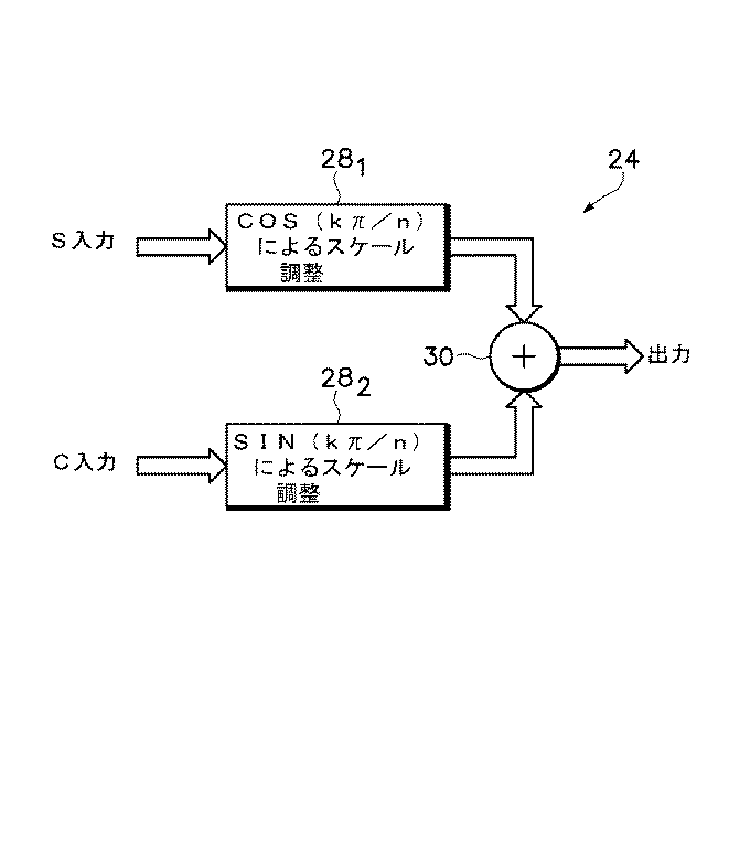
sin(n,ωt)=2n-1Πk=0->n-1(sin(ωt)cos(kπ/n)+cos(ωt)sin(kπ/n))
入力f(t)=sin(ωt)に対して、ヒルベルト変換H()フィルタを用いてcos(ωt)を発生する。ヒルベルト変換フィルタは、目標とする精度を設計入力周波数範囲内として、総ての入力周波数に対してπ/2だけ効果的に位相シフトをできる。フィルタを無限に長くしなければならないので、これは総ての可能な入力周波数に対して動作しない。ヒルベルト変換フィルタを有限インパルス応答(FIR)フィルタとして通常実現するので、これは、線形であり、その入力の総ての位相をπ/2だけ同時に位相シフトできる。入力f(t)に対して、上述の式は、任意の入力用に一般化して、n次の高調波出力を次のように発生する。
Expanding the trigonometric function, this becomes
sin (n, ωt) = 2 n-1 Π k = 0-> n-1 (sin (ωt) cos (kπ / n) + cos (ωt) sin (kπ / n))
For input f (t) = sin (ωt), cos (ωt) is generated using a Hilbert transform H () filter. The Hilbert transform filter can effectively shift the phase by π / 2 with respect to all input frequencies with the target accuracy within the design input frequency range. This does not work for all possible input frequencies since the filter must be infinitely long. Since the Hilbert transform filter is typically implemented as a finite impulse response (FIR) filter, it is linear and can simultaneously phase shift all the phases of its input by π / 2. For the input f (t), the above equation is generalized for an arbitrary input to generate an nth order harmonic output as follows.
ヒルベルト変換フィルタ出力H(f(t))がこの結果のループ変数kから独立しているので、単一のヒルベルト変換フィルタによりこの式の結果を実現できる。実際には、入力フィルタで処理されたf(t)信号を遅延させて、ヒルベルト変換フィルタによる遅延に一致させる。係数cos(kπ/n)及びsin(kπ/n)がkの総ての値に対してf(t)及びH(f(t))の各々を異なるスケールとし、これらを加算して結果の複数の項を生じる。n-1回の掛け算を用いて、これら項の総てを掛け算し、高調波の補正された出力を得る。 Since the Hilbert transform filter output H (f (t)) is independent of the resulting loop variable k, the result of this equation can be realized with a single Hilbert transform filter. In practice, the f (t) signal processed by the input filter is delayed to match the delay by the Hilbert transform filter. The coefficients cos (kπ / n) and sin (kπ / n) are different scales for f (t) and H (f (t)) for all values of k. Generate multiple terms. Multiply all of these terms using n-1 multiplications to obtain the harmonic corrected output.
かかる本発明の直線性補償回路10を図1に示す。なお、入力信号f(t)=sin(ωt)が補償遅延回路12と、高調波補正ユニット142〜14M(以下、包括的に142-Mで示す)の各々に供給される。これら高調波補正ユニット142-Mは、発生手段を構成する。高調波補正ユニット142-M及び補正遅延回路12からの出力を加算器16に供給して、高調波補正信号(高調波が補正された信号)を発生する。これら補正遅延回路12及び加算器16は、加算手段を構成する。
Such a
実施例を考察すると、n=3に対して高調波補正ユニット142-Mで構成された高調波発生手段は、次のように3つの生成物の項に展開される。
Hm(3,f(t))=4(f(t)cos(0)+H(f(t)sin(0))(f(t)cos(π/3)+H(f(t))sin(π/3))(f(t)cos(2π/3)+H(f(t))sin(2π/3))
sin()及びcos()を評価して、次のように簡略化する。
Hm(3,f(t))=4f(t)(f(t)/2+squrt(3)H(f(t))/2)(-f(t)/2+sqrt(3)H(f(t))/2)
なお、squrtは、平方根を意味する。さらに、これを簡略化すると次のようになる。
Hm(3,f(t))=f(t)(3H(f(t))2-f(t)2)
この結果が3次高調波となることを示すために、入力を角周波数ωとして単一の正弦波に設定する。
f(t)=sin(ωt)
ヒルベルト変換フィルタがsin(ωt)をcos(ωt)に変換すると、
H(f(t))=cos(ωt)
となる。以下の既知の多数の角度の展開が、基本波のパワーの点から見て高調波を定義する。
sin(nx)=Σk=0->|_(n-1)/2_|(n,2k+1)(-1)kcos(x)n-1-2ksin(x)2k+1
cos(nx)=Σk=0->|_n/2_|(n,2k)(-1)kcos(x)n-2ksin(x)2k
y=|_x_|は、フロア関数であり、最大の整数y=<xを返す。n=3に対して上述を評価すると、
Hm(3,sin(ωt))=sin(3ωt)
これにより、角周波数ωから直接的に3次高調波角周波数3ωが生じ、他の高調波が生じない。この形式の歪は、上述の如く、又は自己変調メカニズムにより、多項式に分解した非線形性の一部として生じる。
Considering the embodiment, the harmonic generation means constituted by the
Hm (3, f (t)) = 4 (f (t) cos (0) + H (f (t) sin (0)) (f (t) cos (π / 3) + H (f (t) ) sin (π / 3)) (f (t) cos (2π / 3) + H (f (t)) sin (2π / 3))
Evaluate sin () and cos () and simplify as follows.
Hm (3, f (t)) = 4f (t) (f (t) / 2 + squrt (3) H (f (t)) / 2) (-f (t) / 2 + sqrt (3) H (f (t)) / 2)
Note that “squrt” means a square root. Further, this is simplified as follows.
Hm (3, f (t)) = f (t) (3H (f (t)) 2 -f (t) 2 )
In order to show that this result is the third harmonic, the input is set to a single sine wave with an angular frequency ω.
f (t) = sin (ωt)
When the Hilbert transform filter converts sin (ωt) to cos (ωt),
H (f (t)) = cos (ωt)
It becomes. The following known multiple angular expansions define harmonics in terms of fundamental power.
sin (nx) = Σ k = 0-> | _ (n-1) / 2_ | (n, 2k + 1) (-1) k cos (x) n-1-2k sin (x) 2k + 1
cos (nx) = Σ k = 0-> | _n / 2_ | (n, 2k) (-1) k cos (x) n-2k sin (x) 2k
y = | _x_ | is a floor function and returns the maximum integer y = <x. Evaluating the above for n = 3,
Hm (3, sin (ωt)) = sin (3ωt)
As a result, the third harmonic angular frequency 3ω is generated directly from the angular frequency ω, and other harmonics are not generated. This type of distortion occurs as described above or as part of a non-linearity broken down into a polynomial by a self-modulating mechanism.
同様な展開により、正弦波入力から任意の高調波を発生する構造、即ち、アルゴリズムが得られる。パワーを用いるので、サンプル・システムにて、高調波に正確にエリアシングが生じる。上述の多項式システムと同様に、各高調波発生器への入力にフィルタを配置して、入力周波数に応じた各高調波の振幅及び遅延の個別の校正が可能となる。 A similar development yields a structure or algorithm that generates arbitrary harmonics from a sine wave input. Since power is used, the harmonics are accurately aliased in the sample system. Similar to the polynomial system described above, a filter can be placed at the input to each harmonic generator to allow individual calibration of the amplitude and delay of each harmonic according to the input frequency.
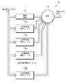
本発明による直線性補償回路用の各高調波補正ユニットのブロック図である図2を参照する。高調波補正ユニット14は、入力振幅及び位相補正フィルタ(入力フィルタ)18を有し、その後段にヒルベルト変換フィルタ20が補償遅延回路22と並列に接続されている。これらヒルベルト変換フィルタ20及び補償遅延回路22は、S(sin)信号(第1信号)及びC(cos)信号(第2信号)を夫々発生し、これら信号は、後段の位相シフト・ユニット240〜24n-1に(以下、包括的に240-(n-1)で示す)に並列に入力する。位相シフト・ユニット240-(n-1)の出力は、高調波補正出力として掛け算器26に供給されて互いにかけ算される。この掛け算器26の出力は、高調波補正ユニット14の出力であり、加算器16(図1)用の入力となる。
Reference is made to FIG. 2, which is a block diagram of each harmonic correction unit for a linearity compensation circuit according to the present invention. The
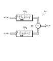
図3は、本発明による直線性補償回路用の位相シフト・ユニットのブロック図である。各位相シフト・ユニット24は、スケール調整回路(スケーラ)281及び282の各々がS入力及びC入力を夫々受ける。S入力に対するスケーラの倍率はcos(kπ/n)であり、C入力に対するスケーラの倍率はsin(kπ/n)である。スケール調整されたS及びC出力は、位相用の加算器30に入力されて加算され、位相シフト・ユニット24からの位相シフト出力を掛け算器26に供給する。
FIG. 3 is a block diagram of a phase shift unit for a linearity compensation circuit according to the present invention. In each
各高調波が他の高調波から独立して校正されるので、この校正手順は、パワーに基づく解法よりも簡単である。まず、振幅/位相補償フィルタ18を高調波校正に対してバイパスするので、これらフィルタが後段の振幅/位相測定との干渉しない。次に、校正は、以下に説明するステップで進む。
This calibration procedure is simpler than the power-based solution because each harmonic is calibrated independently of the other harmonics. First, since the amplitude /
補正すべき非線形歪のn次の各高調波に対して:
関心のある周波数範囲にわたって好ましく等間隔にした1組の補正周波数に対して、
(1)既知の振幅及び周波数の正弦波を非線形システムに入力し、その出力を取込む。
(2)同時に、非線形システムの出力を図2の回路に供給し、n次の高調波を直接発生し、ステップ(1)と同じサンプリング時間で取込む。この回路の入力の歪は、それ自体の結果の歪であるが、これらは、基本波に対して非常に小さいと仮定する。
(3)非線形システムによりステップ(1)及び(2)により発生したn次高調波の相対振幅及び位相を測定する。
For each nth harmonic of the non-linear distortion to be corrected:
For a set of correction frequencies that are preferably equally spaced over the frequency range of interest,
(1) A sine wave having a known amplitude and frequency is input to a nonlinear system and its output is taken.
(2) At the same time, the output of the nonlinear system is supplied to the circuit of FIG. 2, and the nth-order harmonic is directly generated and acquired at the same sampling time as in step (1). Although the distortion of the input of this circuit is a distortion of its own, it is assumed that these are very small relative to the fundamental.
(3) Measure the relative amplitude and phase of the nth-order harmonic generated in steps (1) and (2) by the nonlinear system.
n次高調波での歪発生メカニズムの後で、各校正周波数で得た1組の振幅及び位相補正は、補正用のパラメータを提供する。フィルタが入力のエリアシングのある高調波を補正するために、応答パラメータを変更して、歪発生器の前で、n次高調波振幅/位相補正フィルタ18に適用する。
After the distortion generation mechanism at the nth harmonic, a set of amplitude and phase corrections obtained at each calibration frequency provides the parameters for correction. In order for the filter to correct the input aliasing harmonics, the response parameters are changed and applied to the nth harmonic amplitude /
(4)各相対位相シフトを遅延に変換して(遅延=位相/角周波数)、高調波発生器の前段にフィルタを移動するのに適応させる。
(5)各周波数における相対振幅応答のn次のルートを求める。
(6)ステップ(4)及び(5)で求めた遅延値及び振幅値からデジタル入力フィルタを校正する。一般的には、フィルタは非線形位相の非対称フィルタであるので、設計アプローチの1つは、反復FFTアルゴリズムを用いて、関心のある入力周波数帯域の外側での制約を緩める。よって、規則的に離間した校正周波数にとって好ましい。
(7)ステップ(6)からのn次高調波用に振幅/位相補正フィルタ18をプログラムし、発生した高調波を設定し、それを遅延した入力から減算して、要求されたn次の高調波キャンセルを行う。
(8)直線性補償回路(キャンセル・システム)10を動作させて高調波をキャンセルする。
(4) Convert each relative phase shift into a delay (delay = phase / angular frequency) and adapt it to move the filter to the previous stage of the harmonic generator.
(5) Find the nth order route of the relative amplitude response at each frequency.
(6) The digital input filter is calibrated from the delay value and amplitude value obtained in steps (4) and (5). In general, since the filter is a non-linear phase asymmetric filter, one design approach uses an iterative FFT algorithm to relax constraints outside the input frequency band of interest. It is therefore preferred for regularly spaced calibration frequencies.
(7) Program the amplitude /
(8) The linearity compensation circuit (cancellation system) 10 is operated to cancel harmonics.
本発明は、ヒルベルト変換フィルタ及び位相シフトを用いて関心のある周波数範囲内で各高調波用の個別の高調波補正成分を発生し、これら個別の高調波補正成分を加算して、補正した出力を発生することにより、高調波キャンセルによる直線性補償を行っている。 The present invention uses a Hilbert transform filter and a phase shift to generate individual harmonic correction components for each harmonic within the frequency range of interest, and adds these individual harmonic correction components to provide a corrected output. Therefore, linearity compensation by harmonic cancellation is performed.
10 直線性補償回路
12 補償遅延回路(加算手段の一部)
14 高調波補正ユニット(発生手段)
16 加算器(加算手段の一部)
18 振幅及び位相補正フィルタ(入力フィルタ)
20 ヒルベルト変換フィルタ
22 補償遅延回路
24 位相シフト・ユニット
26 掛け算器
28 スケール調整回路
30 位相加算器
10
14 Harmonic correction unit (generation means)
16 Adder (part of adding means)
18 Amplitude and phase correction filter (input filter)
20
Claims (4)
ヒルベルト変換フィルタを用いて個別に補正された複数の高調波成分を上記入力信号から発生する発生手段と、
上記個別に補正された複数の高調波成分を、遅延させた上記入力信号と加算し、上記高調波歪の高調波をキャンセルして、上記入力信号を補正した出力信号を発生する加算手段と
を具えた直線性補償回路。 A circuit that compensates for the linearity of a nonlinear system that causes harmonic distortion in the input signal,
Generating means for generating a plurality of harmonic components individually corrected using a Hilbert transform filter from the input signal;
Adding means for adding the individually corrected harmonic components to the delayed input signal, canceling harmonics of the harmonic distortion, and generating an output signal in which the input signal is corrected; Provided linearity compensation circuit.
上記高調波補正ユニットの各々は、入力として上記入力信号を受け、出力として上記個別に補正された複数の高調波成分を発生することを特徴とする請求項1の直線性補償回路。 The generating means has a harmonic correction unit for a plurality of harmonics with respect to the fundamental frequency of the input signal,
2. The linearity compensation circuit according to claim 1, wherein each of the harmonic correction units receives the input signal as an input and generates the plurality of individually corrected harmonic components as an output.
上記入力信号を入力として受け、遅延した上記入力信号を出力として発生する回路であって、上記入力信号を遅延して上記高調波補正ユニットの処理時間を補償する入力補償遅延回路と、
上記個別に補償された複数の高調波成分及び上記遅延した入力信号を入力として受け、上記補正した入力信号を出力として発生する加算器と
を有することを特徴とする請求項2の直線性補償回路。 The adding means is
An input compensation delay circuit that receives the input signal as an input and generates the delayed input signal as an output, and delays the input signal to compensate the processing time of the harmonic correction unit;
3. A linearity compensation circuit according to claim 2, further comprising: an adder that receives the plurality of individually compensated harmonic components and the delayed input signal as inputs and generates the corrected input signal as an output. .
上記入力信号を入力として受け、振幅及び位相の補正された上記入力信号を出力として発生する入力フィルタと、
上記振幅及び位相の補正された入力信号を入力として受け、第1信号を出力として発生するヒルベルト変換フィルタと、
上記振幅及び位相の補正された入力信号を遅延させ、第2信号を出力として発生し、上記遅延を上記ヒルベルト変換フィルタの処理時間に等しくさせる手段と、
上記第1信号及び上記第2信号を位相シフトさせ、上記高調波補正ユニット用の所望の高調波を発生し、複数の個別の位相シフトした信号を発生する手段と、
上記複数の個別の位相シフトした信号を掛け算して、上記個別に補正された高調波成分を発生する手段と
を有することを特徴とする請求項2の直線性補償回路。
Each of the above harmonic correction units
An input filter that receives the input signal as an input and generates the input signal with an amplitude and phase corrected as an output;
A Hilbert transform filter that receives the amplitude and phase corrected input signal as an input and generates a first signal as an output;
Means for delaying the amplitude and phase corrected input signal, generating a second signal as an output, and making the delay equal to the processing time of the Hilbert transform filter;
Means for phase shifting the first signal and the second signal to generate a desired harmonic for the harmonic correction unit and to generate a plurality of individual phase shifted signals;
The linearity compensation circuit according to claim 2, further comprising means for multiplying the plurality of individual phase-shifted signals to generate the individually corrected harmonic components.
Applications Claiming Priority (1)
| Application Number | Priority Date | Filing Date | Title |
|---|---|---|---|
| US10/817,203 US6911925B1 (en) | 2004-04-02 | 2004-04-02 | Linearity compensation by harmonic cancellation |
Publications (2)
| Publication Number | Publication Date |
|---|---|
| JP2005295542A true JP2005295542A (en) | 2005-10-20 |
| JP4498184B2 JP4498184B2 (en) | 2010-07-07 |
Family
ID=34679453
Family Applications (1)
| Application Number | Title | Priority Date | Filing Date |
|---|---|---|---|
| JP2005083845A Expired - Lifetime JP4498184B2 (en) | 2004-04-02 | 2005-03-23 | Linearity compensation circuit |
Country Status (4)
| Country | Link |
|---|---|
| US (1) | US6911925B1 (en) |
| EP (1) | EP1583243B1 (en) |
| JP (1) | JP4498184B2 (en) |
| CN (1) | CN1677870B (en) |
Cited By (2)
| Publication number | Priority date | Publication date | Assignee | Title |
|---|---|---|---|---|
| JP2010117338A (en) * | 2008-10-16 | 2010-05-27 | Advantest Corp | Signal processing device, test system, distortion detection device, signal compensation device, analysis signal generator, program, storage medium, distortion detection method, signal compensation method, and analysis signal generation method |
| WO2016006515A1 (en) * | 2014-07-08 | 2016-01-14 | 国立大学法人大阪大学 | Measurement device and measurement method |
Families Citing this family (20)
| Publication number | Priority date | Publication date | Assignee | Title |
|---|---|---|---|---|
| WO2004008808A1 (en) | 2002-07-12 | 2004-01-22 | Ricoh Company, Ltd. | Heating apparatus, auxiliary power supply apparatus, auxiliary power supply system, fixation apparatus, and moving picture formation apparatus |
| US7348908B2 (en) * | 2004-11-04 | 2008-03-25 | Tektronix, Inc. | Linearity corrector using filter products |
| US7161511B2 (en) * | 2005-06-03 | 2007-01-09 | General Electric Company | Linearization system and method |
| US7460043B2 (en) * | 2005-06-03 | 2008-12-02 | General Electric Company | Analog-to-digital converter compensation system and method |
| GB2442265A (en) * | 2006-09-30 | 2008-04-02 | Univ Cardiff | Nonlinear signal processing |
| US20090091487A1 (en) * | 2007-10-04 | 2009-04-09 | Texas Instruments Incorporated | Spurious Free Dynamic Range Of An Analog To Digital Converter |
| US8625813B2 (en) * | 2008-12-23 | 2014-01-07 | Stmicroelectronics, Inc. | Asymmetric polynomial psychoacoustic bass enhancement |
| JP5609684B2 (en) * | 2011-02-01 | 2014-10-22 | ソニー株式会社 | AD converter and signal processing system |
| CN103023498A (en) * | 2012-12-31 | 2013-04-03 | 深圳市九洲电器有限公司 | Method and device for improving non-linear distortion performance of digital-to-analog converter |
| US9112457B1 (en) | 2013-01-29 | 2015-08-18 | Teledyne Lecroy, Inc. | Decompressor |
| CN107040214B (en) * | 2017-03-03 | 2021-01-29 | 北京东方计量测试研究所 | Low stray sinusoidal signal generator based on multi-point compensation scheme |
| US11489847B1 (en) * | 2018-02-14 | 2022-11-01 | Nokomis, Inc. | System and method for physically detecting, identifying, and diagnosing medical electronic devices connectable to a network |
| US10574250B1 (en) * | 2019-02-28 | 2020-02-25 | Nxp Usa, Inc. | Digital calibration systems and methods for multi-stage analog-to-digital converters |
| CN111277267A (en) * | 2020-03-05 | 2020-06-12 | 中国人民解放军国防科技大学 | Delay mismatch compensation method, device and electronic equipment for dual-channel TIADC |
| CN111682912B (en) * | 2020-05-29 | 2022-03-08 | 中国科学院微电子研究所 | Ultra-wideband power amplifier harmonic wave elimination device and method based on FPGA |
| CN112084732B (en) * | 2020-08-12 | 2024-03-01 | 中电科思仪科技股份有限公司 | A harmonic compensation method based on FPGA |
| EP4275231B1 (en) | 2021-01-11 | 2025-04-30 | YSI, Inc. | Optical sensor with induced crosstalk circuit for improved sensor linearity |
| CN112763769B (en) * | 2021-04-08 | 2021-07-06 | 深圳市鼎阳科技股份有限公司 | A signal generator with ultra-low harmonic distortion |
| CN114123205B (en) * | 2021-11-01 | 2023-12-22 | 深圳供电局有限公司 | Harmonic compensation system and phase correction method and device thereof |
| CN114283857B (en) * | 2021-12-16 | 2024-05-28 | 上海艾为电子技术股份有限公司 | Delay compensation of frequency division signal, frequency division method, system and frequency divider |
Citations (6)
| Publication number | Priority date | Publication date | Assignee | Title |
|---|---|---|---|---|
| JPS61129908A (en) * | 1984-11-28 | 1986-06-17 | Toshiba Corp | Three-multiple circuit |
| JPS63121916U (en) * | 1987-01-30 | 1988-08-08 | ||
| JPH07321613A (en) * | 1994-05-24 | 1995-12-08 | Kokusai Electric Co Ltd | Frequency multiplier, waveform shaping circuit, variable phase shift circuit |
| JPH10303708A (en) * | 1997-04-24 | 1998-11-13 | Nec Corp | Frequency multiplier circuit |
| JPH1117749A (en) * | 1997-06-24 | 1999-01-22 | Nec Corp | Demodulation circuit |
| JP2003133959A (en) * | 2001-10-29 | 2003-05-09 | Sony Corp | D / A converter and output amplifier circuit |
Family Cites Families (11)
| Publication number | Priority date | Publication date | Assignee | Title |
|---|---|---|---|---|
| US4615038A (en) * | 1984-06-06 | 1986-09-30 | At&T Information Systems Inc. | Equalization of modulated data signals utilizing tentative and final decisions and replication of non-linear channel distortion |
| JPH07118649B2 (en) | 1986-01-08 | 1995-12-18 | ヤマハ株式会社 | Dither circuit |
| US5168526A (en) * | 1990-10-29 | 1992-12-01 | Akg Acoustics, Inc. | Distortion-cancellation circuit for audio peak limiting |
| GB9026906D0 (en) * | 1990-12-11 | 1991-01-30 | B & W Loudspeakers | Compensating filters |
| US5196851A (en) * | 1991-05-24 | 1993-03-23 | Samsung Electronics Co., Ltd. | Linearizing non-linear analog-to-digital process and circuit |
| US5617058A (en) * | 1995-11-13 | 1997-04-01 | Apogee Technology, Inc. | Digital signal processing for linearization of small input signals to a tri-state power switch |
| US6177893B1 (en) * | 1998-09-15 | 2001-01-23 | Scott R. Velazquez | Parallel processing analog and digital converter |
| US6198416B1 (en) | 1999-04-16 | 2001-03-06 | Scott R. Velazquez | Linearity error compensator |
| US6584205B1 (en) * | 1999-08-26 | 2003-06-24 | American Technology Corporation | Modulator processing for a parametric speaker system |
| US6424275B1 (en) | 2001-01-18 | 2002-07-23 | Scott R. Velazquez | Linearity error compensator |
| US6570514B1 (en) | 2001-12-21 | 2003-05-27 | Scott R. Velazquez | Linearity error compensator |
-
2004
- 2004-04-02 US US10/817,203 patent/US6911925B1/en not_active Expired - Lifetime
-
2005
- 2005-03-23 JP JP2005083845A patent/JP4498184B2/en not_active Expired - Lifetime
- 2005-04-01 CN CN2005100651465A patent/CN1677870B/en not_active Expired - Lifetime
- 2005-04-01 EP EP05252069.9A patent/EP1583243B1/en not_active Expired - Lifetime
Patent Citations (6)
| Publication number | Priority date | Publication date | Assignee | Title |
|---|---|---|---|---|
| JPS61129908A (en) * | 1984-11-28 | 1986-06-17 | Toshiba Corp | Three-multiple circuit |
| JPS63121916U (en) * | 1987-01-30 | 1988-08-08 | ||
| JPH07321613A (en) * | 1994-05-24 | 1995-12-08 | Kokusai Electric Co Ltd | Frequency multiplier, waveform shaping circuit, variable phase shift circuit |
| JPH10303708A (en) * | 1997-04-24 | 1998-11-13 | Nec Corp | Frequency multiplier circuit |
| JPH1117749A (en) * | 1997-06-24 | 1999-01-22 | Nec Corp | Demodulation circuit |
| JP2003133959A (en) * | 2001-10-29 | 2003-05-09 | Sony Corp | D / A converter and output amplifier circuit |
Cited By (4)
| Publication number | Priority date | Publication date | Assignee | Title |
|---|---|---|---|---|
| JP2010117338A (en) * | 2008-10-16 | 2010-05-27 | Advantest Corp | Signal processing device, test system, distortion detection device, signal compensation device, analysis signal generator, program, storage medium, distortion detection method, signal compensation method, and analysis signal generation method |
| WO2016006515A1 (en) * | 2014-07-08 | 2016-01-14 | 国立大学法人大阪大学 | Measurement device and measurement method |
| JPWO2016006515A1 (en) * | 2014-07-08 | 2017-04-27 | 国立大学法人大阪大学 | Measuring device and measuring method |
| US10241031B2 (en) | 2014-07-08 | 2019-03-26 | Osaka University | Measuring device and measuring method |
Also Published As
| Publication number | Publication date |
|---|---|
| EP1583243A3 (en) | 2006-06-28 |
| CN1677870A (en) | 2005-10-05 |
| CN1677870B (en) | 2010-06-09 |
| EP1583243A2 (en) | 2005-10-05 |
| JP4498184B2 (en) | 2010-07-07 |
| US6911925B1 (en) | 2005-06-28 |
| EP1583243B1 (en) | 2017-06-07 |
Similar Documents
| Publication | Publication Date | Title |
|---|---|---|
| JP4498184B2 (en) | Linearity compensation circuit | |
| US8917125B1 (en) | Interleaving analog-to-digital converter (ADC) with background calibration | |
| US7394415B2 (en) | Time-interleaved analog-to-digital converter and high speed signal processing system using the same | |
| JP4754941B2 (en) | Linear corrector | |
| CN111384950B (en) | Linear and nonlinear calibration for time-interleaved digital-to-analog converters | |
| US9030340B1 (en) | N-path interleaving analog-to-digital converter (ADC) with background calibration | |
| CN109936366B (en) | Signal path linearization | |
| CN107959499B (en) | Measuring and correcting system non-idealities | |
| EP2359479B1 (en) | Methods and apparatuses for estimation and compensation of nonlinearity errors | |
| JP2014103671A (en) | Calibration method of rf signal source and amplitude flatness and phase linearity calibration unit | |
| JP3752237B2 (en) | A / D converter | |
| JP4076547B2 (en) | Dither circuit for quantizer | |
| US9166610B2 (en) | Converter arrangement and method for converting an analogue input signal into a digital output signal | |
| US9292035B2 (en) | Packet based DDS minimizing mathematical and DAC noise | |
| JP4451486B2 (en) | Analog / digital conversion device and digital / analog conversion device | |
| JP7734235B2 (en) | Correction system for eliminating the effects of phase noise and analog-to-digital conversion device including the same | |
| US20130271155A1 (en) | Impedance measurement device and method | |
| Soudan et al. | Correction structures for linear weakly time-varying systems | |
| US11695424B2 (en) | Distortion reduction circuit | |
| EP1542366A1 (en) | ADC with digital error correction | |
| JP2006279425A (en) | A/d converter | |
| JP6512092B2 (en) | Frequency characteristic correction circuit | |
| Mankovskyy et al. | Digital Method of SSB Modulation | |
| CN121887186A (en) | TI ADC time-skewed background calibration using complex derivative signals | |
| US9112457B1 (en) | Decompressor |
Legal Events
| Date | Code | Title | Description |
|---|---|---|---|
| RD04 | Notification of resignation of power of attorney |
Free format text: JAPANESE INTERMEDIATE CODE: A7424 Effective date: 20060616 |
|
| A625 | Written request for application examination (by other person) |
Free format text: JAPANESE INTERMEDIATE CODE: A625 Effective date: 20070220 |
|
| A131 | Notification of reasons for refusal |
Free format text: JAPANESE INTERMEDIATE CODE: A131 Effective date: 20090616 |
|
| A521 | Request for written amendment filed |
Free format text: JAPANESE INTERMEDIATE CODE: A523 Effective date: 20090727 |
|
| A131 | Notification of reasons for refusal |
Free format text: JAPANESE INTERMEDIATE CODE: A131 Effective date: 20090929 |
|
| A521 | Request for written amendment filed |
Free format text: JAPANESE INTERMEDIATE CODE: A523 Effective date: 20091216 |
|
| A131 | Notification of reasons for refusal |
Free format text: JAPANESE INTERMEDIATE CODE: A131 Effective date: 20100119 |
|
| A521 | Request for written amendment filed |
Free format text: JAPANESE INTERMEDIATE CODE: A523 Effective date: 20100308 |
|
| TRDD | Decision of grant or rejection written | ||
| A01 | Written decision to grant a patent or to grant a registration (utility model) |
Free format text: JAPANESE INTERMEDIATE CODE: A01 Effective date: 20100413 |
|
| A01 | Written decision to grant a patent or to grant a registration (utility model) |
Free format text: JAPANESE INTERMEDIATE CODE: A01 |
|
| A61 | First payment of annual fees (during grant procedure) |
Free format text: JAPANESE INTERMEDIATE CODE: A61 Effective date: 20100413 |
|
| FPAY | Renewal fee payment (event date is renewal date of database) |
Free format text: PAYMENT UNTIL: 20130423 Year of fee payment: 3 |
|
| R150 | Certificate of patent or registration of utility model |
Ref document number: 4498184 Country of ref document: JP Free format text: JAPANESE INTERMEDIATE CODE: R150 Free format text: JAPANESE INTERMEDIATE CODE: R150 |
|
| R250 | Receipt of annual fees |
Free format text: JAPANESE INTERMEDIATE CODE: R250 |
|
| R250 | Receipt of annual fees |
Free format text: JAPANESE INTERMEDIATE CODE: R250 |
|
| R250 | Receipt of annual fees |
Free format text: JAPANESE INTERMEDIATE CODE: R250 |
|
| R250 | Receipt of annual fees |
Free format text: JAPANESE INTERMEDIATE CODE: R250 |
|
| R250 | Receipt of annual fees |
Free format text: JAPANESE INTERMEDIATE CODE: R250 |
|
| R250 | Receipt of annual fees |
Free format text: JAPANESE INTERMEDIATE CODE: R250 |
|
| R250 | Receipt of annual fees |
Free format text: JAPANESE INTERMEDIATE CODE: R250 |
|
| R250 | Receipt of annual fees |
Free format text: JAPANESE INTERMEDIATE CODE: R250 |
|
| R250 | Receipt of annual fees |
Free format text: JAPANESE INTERMEDIATE CODE: R250 |
|
| R250 | Receipt of annual fees |
Free format text: JAPANESE INTERMEDIATE CODE: R250 |
|
| R250 | Receipt of annual fees |
Free format text: JAPANESE INTERMEDIATE CODE: R250 |
|
| R250 | Receipt of annual fees |
Free format text: JAPANESE INTERMEDIATE CODE: R250 |
|
| EXPY | Cancellation because of completion of term |