JP2005296960A - Metal surface treatment agent, metal surface treatment method, solder bonding agent, solder paste, and semiconductor electronic component mounting method - Google Patents
Metal surface treatment agent, metal surface treatment method, solder bonding agent, solder paste, and semiconductor electronic component mounting method Download PDFInfo
- Publication number
- JP2005296960A JP2005296960A JP2004112358A JP2004112358A JP2005296960A JP 2005296960 A JP2005296960 A JP 2005296960A JP 2004112358 A JP2004112358 A JP 2004112358A JP 2004112358 A JP2004112358 A JP 2004112358A JP 2005296960 A JP2005296960 A JP 2005296960A
- Authority
- JP
- Japan
- Prior art keywords
- solder
- metal surface
- surface treatment
- metal
- electronic component
- Prior art date
- Legal status (The legal status is an assumption and is not a legal conclusion. Google has not performed a legal analysis and makes no representation as to the accuracy of the status listed.)
- Withdrawn
Links
- 229910000679 solder Inorganic materials 0.000 title claims abstract description 103
- 239000002184 metal Substances 0.000 title claims abstract description 84
- 229910052751 metal Inorganic materials 0.000 title claims abstract description 84
- 238000000034 method Methods 0.000 title claims abstract description 28
- 239000004065 semiconductor Substances 0.000 title claims abstract description 24
- 239000012756 surface treatment agent Substances 0.000 title claims description 30
- 239000007767 bonding agent Substances 0.000 title claims description 28
- 238000004381 surface treatment Methods 0.000 title claims description 7
- 239000000463 material Substances 0.000 claims abstract description 23
- 239000000843 powder Substances 0.000 claims abstract description 23
- 239000003795 chemical substances by application Substances 0.000 claims abstract description 13
- 238000006467 substitution reaction Methods 0.000 claims abstract description 6
- 238000004898 kneading Methods 0.000 claims description 11
- 150000001875 compounds Chemical class 0.000 claims description 10
- -1 acetic acid compound Chemical class 0.000 claims description 9
- 238000010438 heat treatment Methods 0.000 claims description 9
- 150000002366 halogen compounds Chemical class 0.000 claims description 8
- QTBSBXVTEAMEQO-UHFFFAOYSA-N Acetic acid Natural products CC(O)=O QTBSBXVTEAMEQO-UHFFFAOYSA-N 0.000 claims description 6
- 239000011230 binding agent Substances 0.000 claims description 6
- 229910052759 nickel Inorganic materials 0.000 claims description 5
- 229910052782 aluminium Inorganic materials 0.000 claims description 4
- 229910052802 copper Inorganic materials 0.000 claims description 4
- 229910052737 gold Inorganic materials 0.000 claims description 4
- 150000002736 metal compounds Chemical class 0.000 claims description 4
- 229910052709 silver Inorganic materials 0.000 claims description 4
- 229910052718 tin Inorganic materials 0.000 claims description 4
- 229910052725 zinc Inorganic materials 0.000 claims description 4
- 229910017604 nitric acid Inorganic materials 0.000 claims description 3
- QAOWNCQODCNURD-UHFFFAOYSA-N sulfuric acid Substances OS(O)(=O)=O QAOWNCQODCNURD-UHFFFAOYSA-N 0.000 claims description 3
- 238000005476 soldering Methods 0.000 abstract description 7
- 239000007769 metal material Substances 0.000 abstract 2
- 239000004568 cement Substances 0.000 abstract 1
- 229940125782 compound 2 Drugs 0.000 abstract 1
- 230000002708 enhancing effect Effects 0.000 abstract 1
- 239000010949 copper Substances 0.000 description 18
- XEEYBQQBJWHFJM-UHFFFAOYSA-N iron Substances [Fe] XEEYBQQBJWHFJM-UHFFFAOYSA-N 0.000 description 7
- 229910021591 Copper(I) chloride Inorganic materials 0.000 description 5
- OXBLHERUFWYNTN-UHFFFAOYSA-M copper(I) chloride Chemical compound [Cu]Cl OXBLHERUFWYNTN-UHFFFAOYSA-M 0.000 description 5
- 238000010586 diagram Methods 0.000 description 5
- 230000004907 flux Effects 0.000 description 5
- 238000006243 chemical reaction Methods 0.000 description 3
- 150000002739 metals Chemical class 0.000 description 3
- 239000012190 activator Substances 0.000 description 2
- 229910045601 alloy Inorganic materials 0.000 description 2
- 239000000956 alloy Substances 0.000 description 2
- 239000010953 base metal Substances 0.000 description 2
- 229910052804 chromium Inorganic materials 0.000 description 2
- 230000003647 oxidation Effects 0.000 description 2
- 238000007254 oxidation reaction Methods 0.000 description 2
- 238000007747 plating Methods 0.000 description 2
- 238000009736 wetting Methods 0.000 description 2
- 229910001018 Cast iron Inorganic materials 0.000 description 1
- RYGMFSIKBFXOCR-UHFFFAOYSA-N Copper Chemical compound [Cu] RYGMFSIKBFXOCR-UHFFFAOYSA-N 0.000 description 1
- ISWSIDIOOBJBQZ-UHFFFAOYSA-N Phenol Chemical compound OC1=CC=CC=C1 ISWSIDIOOBJBQZ-UHFFFAOYSA-N 0.000 description 1
- 229910020830 Sn-Bi Inorganic materials 0.000 description 1
- 229910018728 Sn—Bi Inorganic materials 0.000 description 1
- QVGXLLKOCUKJST-UHFFFAOYSA-N atomic oxygen Chemical compound [O] QVGXLLKOCUKJST-UHFFFAOYSA-N 0.000 description 1
- 239000000470 constituent Substances 0.000 description 1
- 230000006866 deterioration Effects 0.000 description 1
- 230000000694 effects Effects 0.000 description 1
- 239000003822 epoxy resin Substances 0.000 description 1
- 229910052742 iron Inorganic materials 0.000 description 1
- 238000002844 melting Methods 0.000 description 1
- 230000008018 melting Effects 0.000 description 1
- 239000000203 mixture Substances 0.000 description 1
- 229910052760 oxygen Inorganic materials 0.000 description 1
- 239000001301 oxygen Substances 0.000 description 1
- 229920000647 polyepoxide Polymers 0.000 description 1
- 229920000728 polyester Polymers 0.000 description 1
- 238000007639 printing Methods 0.000 description 1
- 229920005989 resin Polymers 0.000 description 1
- 239000011347 resin Substances 0.000 description 1
- 238000007650 screen-printing Methods 0.000 description 1
- 238000007789 sealing Methods 0.000 description 1
- 238000004544 sputter deposition Methods 0.000 description 1
- 239000000758 substrate Substances 0.000 description 1
Images
Landscapes
- Electric Connection Of Electric Components To Printed Circuits (AREA)
Abstract
Description
本発明は、金属表面処理剤、金属表面処理方法、はんだ接合剤、はんだペースト及び半導体電子部品の実装方法に関し、更に詳しくは、はんだ接合性の向上を図る技術に関する。 The present invention relates to a metal surface treatment agent, a metal surface treatment method, a solder bonding agent, a solder paste, and a semiconductor electronic component mounting method, and more particularly to a technique for improving solder bonding properties.
従来より電子部品をプリント基板などに接合する際には、基板上のランドにはんだペーストを印刷後、マウンターなどの搭載機で電子部品を搭載し、その後、リフロー炉内ではんだペースト(はんだ粉とフラックスとを混練して構成される)を溶融することによりはんだ付けを行っている。基板上のランドの金属表面には、空気中の酸素に触れて酸化膜が形成されており、この酸化膜は接合不良などの不都合を発生させることから、従来のはんだペースト内のフラックスには、酸化膜を除去するための活性剤が混合されている。この種のフラックスを有するはんだペーストにおいては、強固な接合が得られるように接合部に対する濡れ性の向上が望まれており、従来は、フラックスに含有する活性剤の含有量を変えるなどしてはんだ濡れ性を改善するようにしていた(例えば、特許文献1参照)。 Conventionally, when joining electronic parts to printed circuit boards, etc., after printing the solder paste on the lands on the board, the electronic parts are mounted on a mounting machine such as a mounter, and then solder paste (solder powder and Soldering is performed by melting (made up by kneading flux). On the metal surface of the land on the substrate, an oxide film is formed by contact with oxygen in the air, and this oxide film causes inconvenience such as poor bonding, so the flux in the conventional solder paste includes An activator for removing the oxide film is mixed. In a solder paste having this kind of flux, improvement in wettability with respect to the joint portion is desired so that a strong joint can be obtained. Conventionally, soldering is performed by changing the content of the activator contained in the flux. The wettability was improved (for example, see Patent Document 1).
しかしながら上記特許文献1の技術は、あくまでもはんだが濡れる性質を有する金属を接合対象とした場合に、はんだ濡れ性を改善することを目的としたものであった。したがって、例えばSUS材のように、はんだが全く濡れない金属に対して上記従来のはんだペーストを用いたとしても、濡れ性の改善どころか接合自体が不可能であった。この種のはんだが濡れない金属をはんだによって接合可能とするためには、はんだが濡れない金属の表面に、はんだが濡れやすい膜を形成し、その膜を用いてはんだ接合する方法が一つとして考えられる。このような膜形成に際しては、例えばスパッタ装置を用いて真空中で形成する方法が一般的に用いられるが、この方法は装置が大掛かりとなりコスト高となるなどの不都合があった。
However, the technique disclosed in
本発明はこのような点に鑑みなされたもので、はんだが濡れない金属表面に、はんだが濡れる膜を簡単に形成できて被接合部材との接合性を高めることが可能な金属表面処理剤、金属表面処理方法、はんだ接合剤、はんだペースト及び半導体電子部品の実装方法を提供することを目的とする。 The present invention has been made in view of such points, a metal surface treatment agent capable of easily forming a film on which solder is wetted on a metal surface on which solder is not wettable and improving the bondability with a member to be joined, An object is to provide a metal surface treatment method, a solder bonding agent, a solder paste, and a semiconductor electronic component mounting method.
本発明に係る金属表面処理剤は、加熱された際に、母材を構成する金属成分と置換反応を起こす性質を有する金属であって、且つはんだとの濡れ性が良い金属の化合物の粉末が含有されてなるものである。
これにより、はんだが濡れない金属表面に、金属表面処理剤を塗布して加熱することで、簡単に、はんだ濡れ性の良い金属層を形成することができる。したがって、この金属層を用いてはんだ接合することにより、被接合部材との接合性を高めることが可能となる。
The metal surface treatment agent according to the present invention is a metal compound powder having a property of causing a substitution reaction with a metal component constituting a base material when heated, and a metal compound powder having good wettability with solder. It is contained.
Thereby, a metal layer with good solder wettability can be easily formed by applying and heating a metal surface treatment agent on a metal surface on which solder does not wet. Therefore, it is possible to improve the bondability with the member to be joined by soldering using this metal layer.
また、本発明に係る金属表面処理剤は、上記化合物の粉末と有機バインダーとが混練されてなるものである。
このように、金属表面処理剤は、化合物の粉末と有機バインダーとが混練されてペースト状に構成される。
Further, the metal surface treatment agent according to the present invention is obtained by kneading the above-mentioned compound powder and an organic binder.
As described above, the metal surface treatment agent is formed into a paste by kneading the compound powder and the organic binder.
また、本発明に係る金属表面処理剤は、上記金属が、Cu,Sn,Ag,Au,Ni,Zn,Al又はCrの何れかであるものである。 In the metal surface treatment agent according to the present invention, the metal is any one of Cu, Sn, Ag, Au, Ni, Zn, Al, or Cr.
また、本発明に係る金属表面処理剤は、上記化合物がハロゲン化合物、酢酸化合物、硝酸化合物又は硫酸化合物の何れかであるものである。 In the metal surface treating agent according to the present invention, the compound is any one of a halogen compound, an acetic acid compound, a nitric acid compound, or a sulfuric acid compound.
本発明に係る金属表面処理方法は、母材表面に金属表面処理剤を塗布した後、加熱装置内で加熱するものである。
このようにして、はんだが濡れない母材表面に、はんだ濡れ性の良い金属層を形成することができる。
In the metal surface treatment method according to the present invention, a metal surface treatment agent is applied to the surface of a base material and then heated in a heating device.
In this way, a metal layer with good solder wettability can be formed on the surface of the base material on which the solder does not wet.
本発明に係るはんだ接合剤は、上記の何れかの金属表面処理剤と、はんだ粉とを混練してなるものである。
このはんだ接合剤を用いてはんだ接合を行うことにより、はんだが濡れない母材金属であっても、被接合部材とのはんだ接合が可能となる。
The solder bonding agent according to the present invention is obtained by kneading any of the above metal surface treatment agents and solder powder.
By performing solder bonding using this solder bonding agent, it is possible to perform solder bonding with a member to be bonded even if the base metal is not wetted by solder.
本発明に係るはんだペーストは、上記の何れかの金属表面処理剤を含有してなるものである。
このはんだペーストを用いてはんだ接合を行うことにより、はんだが濡れない母材金属であっても、被接合部材とのはんだ接合が可能となる。
The solder paste according to the present invention contains any of the above-described metal surface treatment agents.
By performing solder bonding using this solder paste, solder bonding with a member to be bonded is possible even if the base metal is a metal that does not wet the solder.
本発明に係る半導体電子部品の実装方法は、上記のはんだ接合剤を用いて半導体電子部品を配線基板上に接合するものである。
また、本発明に係る半導体電子部品の実装方法は、上記のはんだペーストを用いて半導体電子部品を配線基板上に接合するものである。
この実装方法によれば、半導体電子部品のリードにはんだ濡れ性を向上させるメッキが施されていなくても、上記のはんだ接合剤を用いることによりはんだ濡れ性が向上して良好な接合が可能となり、信頼性の高い半導体電子部品の実装が可能となる。
The semiconductor electronic component mounting method according to the present invention is a method for bonding a semiconductor electronic component onto a wiring board using the solder bonding agent.
Moreover, the mounting method of the semiconductor electronic component which concerns on this invention joins a semiconductor electronic component on a wiring board using said solder paste.
According to this mounting method, even if the lead of the semiconductor electronic component is not plated to improve the solder wettability, the solder wettability is improved by using the above-mentioned solder bonding agent, and good bonding is possible. This makes it possible to mount highly reliable semiconductor electronic components.
実施の形態1.
以下、本発明の実施の形態1に係る金属表面処理剤について説明する。
本実施の形態1の金属表面処理剤は、加熱された際に、母材を構成する金属成分と置換反応を生じる性質を有する金属であって、且つはんだとの濡れ性が良い金属の化合物の粉末が含有されてなるものである。
ここで、はんだとの濡れ性の良い金属とは、Cu,Sn,Ag,Au,Ni,Zn,Al又はCrなどが該当し、これら各金属は、はんだ濡れ性の良い金属として従来より知られたものである。また、化合物としては、例えばハロゲン化合物、酢酸化合物、硝酸化合物又は硫酸化合物などが該当する。本例の金属表面処理剤は、前記化合物の粉末と、例えばエポキシ樹脂、ポリエステル又はフェノールなどの有機バインダーとを混練して構成されており、ペースト状に構成されている。
Hereinafter, the metal surface treatment agent according to
The metal surface treatment agent of the first embodiment is a metal compound having a property of causing a substitution reaction with a metal component constituting a base material when heated, and having good wettability with solder. It contains powder.
Here, the metal having good wettability with solder includes Cu, Sn, Ag, Au, Ni, Zn, Al, Cr, etc., and these metals are conventionally known as metals having good solder wettability. It is a thing. Further, examples of the compound include a halogen compound, an acetic acid compound, a nitric acid compound, and a sulfuric acid compound. The metal surface treating agent of this example is configured by kneading the powder of the compound and an organic binder such as epoxy resin, polyester, or phenol, and is configured in a paste form.
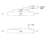
図1は、本発明の実施の形態1に係る金属表面処理剤による表面処理方法を説明する模式図である。本例ではSUS材を母材とし、特にSUS304とする場合を例に説明する。SUS304の組成は、Fe−18Cr−8Ni(74wt%のFeと18wt%のCrと8Ni)である。
SUS材10の表面に金属表面処理剤1を塗布する(図1(a))。金属表面処理剤1は、ここではCuをハロゲン化合物化した化合物(CuCl2 )2の粉末と有機バインダー3とを混練したものである。金属表面処理剤1を塗布した後、全体をリフロー炉等の加熱装置に挿入して加熱する(図示省略)。これによりSUS材10表面と金属表面処理剤1との間で以下に示す化学反応が生じる。
FIG. 1 is a schematic diagram for explaining a surface treatment method using a metal surface treatment agent according to
The metal
すなわち、加熱されることによりSUS材10を構成するFe成分とハロゲン化合物(CuCl2 )2とが次式(1)で示すような置換反応を起こし、その結果、SUS材10の表面にCu層10aが析出される(図1(b))。
That is, when heated, the Fe component constituting the
CuCl2 + Fe → Cu+FeCl2 ・・・ (1) CuCl 2 + Fe → Cu + FeCl 2 (1)
このように、SUS材10表面にCu層10aが形成される。このCu層10aは、はんだ濡れ性の良い金属層であることから、このCu層10aを利用して既存のはんだペーストを用いた接合が可能となる。
Thus, the
このように実施の形態1によれば、はんだが濡れない金属表面に、金属表面処理剤1を塗布して加熱することで、簡単に、はんだ濡れ性の良い金属層を形成することができる。したがって、この金属層を用いてはんだ接合することにより、被接合部材との接合性が高まり、良好な接合を行うことが可能となる。
As described above, according to the first embodiment, a metal layer with good solder wettability can be easily formed by applying the metal
なお、本例では、Cuのハロゲン化合物(CuCl2 )の粉末を含有した金属表面処理剤1を例に挙げて説明したが、本発明の金属表面処理剤に含有される化合物は、上述したように他にSn,Ag,Au,Ni,Zn,AlあるいはCrなどの化合物としても良く、例えばSnのハロゲン化合物(SnCl2 )としても良い。この場合、SUS材10表面にSn層が形成されることになる。このSn層も、はんだ濡れ性の良い金属層であるため、Cu層10aの場合と同様に、被接合部材との接合性が高まり、良好な接合を行うことが可能となる。
In this example, the metal
また、はんだが濡れない金属として、SUS材を例に挙げて説明したが、これに限られたものではなく、他に例えばFe系の金属(鋳鉄など)なども含まれる。このFe系の金属表面上にも、本発明の金属表面処理剤1を用いて同様に処理することで、はんだ濡れ性の良い金属層を形成することができる。
In addition, although the SUS material has been described as an example of the metal that does not wet the solder, it is not limited to this, and other examples include, for example, an Fe-based metal (such as cast iron). A metal layer having good solder wettability can be formed on the Fe-based metal surface by the same treatment using the metal
実施の形態2.
次に、実施の形態1の金属表面処理剤1とはんだ粉とを混練して構成したはんだ接合剤を用いてはんだ接合を実施する場合の処理工程を説明する。
Next, processing steps in the case of performing solder bonding using a solder bonding agent constituted by kneading the metal
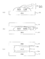
図2は、はんだ接合剤を用いてはんだ接合を実施する場合の処理工程を示す模式図である。なお、本例ではSUS材同士を接合する場合を例に説明する。
まず、SUS材11の表面に、金属表面処理剤1とはんだ粉4とを混練してなるはんだ接合剤20を塗布する(図2(a))。その上に接合対象のSUS材12を載置する(図2(b))。そして、その状態でリフロー炉等の加熱装置(図示せず)内に挿入して全体を加熱する(図示省略)。これにより、はんだ接合剤20が加熱されて溶解し、はんだ接合剤20とSUS材11,12のそれぞれの表面金属との間で上記(1)式で示したのと同じ化学反応が生じてCu層11a,12aが析出される。SUS材11,12表面に析出したCu層11a,12aは、はんだ濡れ性が良いため、このCu層11a,12aに、溶融したはんだ21が濡れ広がって(図2(c))、良好な接合が得られる。
FIG. 2 is a schematic diagram illustrating a processing step in the case of performing solder bonding using a solder bonding agent. In this example, a case where SUS materials are joined to each other will be described as an example.
First, a
このように実施の形態2によれば、金属表面処理剤1とはんだ粉4とを混練してなるはんだ接合剤20を用いることにより、従来、はんだ濡れ性が無くはんだによる接合が不可能であった金属をはんだ接合することが可能となる。
As described above, according to the second embodiment, by using the
実施の形態3.
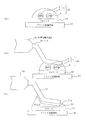
次に、実施の形態2のはんだ接合剤20を用いた半導体電子部品の実装工程を説明する。なお、実装される半導体電子部品は、半導体チップを内部に樹脂封止した樹脂封止部の側面からリードが延出されたQFP等の構成のものであるとする。また、リードは42alloy等で構成されており、通常リードには、はんだ濡れ性を向上させるために例えばSn−Bi等のメッキが施されている。しかしながら、本例のはんだ接合剤20を用いる場合には、このメッキは不要となり、リードの構成金属そのものの表面に、直接、はんだ接合剤20を塗布してはんだ接合することになる。
Next, a semiconductor electronic component mounting process using the
図3は、半導体電子部品の実装工程を説明する模式図である。なお、リードはここでは42alloy(58wt%Fe−42wt%Ni)で構成されているものとする。
半導体電子部品30を実装する際には、まず、プリント配線基板41の金属ランド42(図3にはCu(銅)ランドを例示。他に例えばAuランドとしても良い)上に、はんだ接合剤20をスクリーン印刷等で供給/塗布する(図3(a))。そして、マウンターなどの搭載機でリード31を有する半導体電子部品30をプリント配線基板41上に搭載する(図3(b))。その後、この状態でリフロー炉等の加熱装置(図示せず)内に挿入する。これにより、はんだ接合剤20が溶解し、はんだ接合剤20とリード31のFe成分との間で上記(1)に示した化学反応が生じる。
FIG. 3 is a schematic view for explaining the mounting process of the semiconductor electronic component. Here, the lead is assumed to be composed of 42 alloy (58 wt% Fe-42 wt% Ni).
When mounting the semiconductor
すなわち、加熱装置内で加熱されることにより、リード31のFe成分とはんだ接合剤20中のハロゲン化合物(CuCl2 )2が(1)式で示した置換反応を起こし、その結果、リード31表面にCu層31aが析出され、析出したCu層31aは、はんだ濡れ性が良いため、溶融したはんだ21がこのCu層31aに濡れ広がり(図3(c))、良好な接合が得られる。
That is, by heating in the heating device, the Fe component of the
以上説明したように、半導体電子部品30の実装に際し、前述したはんだ接合剤20を用いることにより、従来、はんだ濡れ性向上のためにリード31に設けられていたメッキが不要となりながらも、はんだ濡れ性が向上して良好な接合が可能となり、信頼性の高い半導体電子部品30の実装が可能である。
As described above, when the semiconductor
また、金属表面処理剤1中には、はんだ濡れ性の良い金属粉が化合物化されて含有されているので、その金属粉の酸化を防ぐことが可能である。したがって、金属粉の酸化による、はんだ接合剤20保存中の劣化やはんだ濡れ性の低下を防止でき、保存安定性が良く、良好なはんだ付けが可能なはんだ接合剤20を得ることができる。
In addition, since the metal
なお、上記実施の形態では、金属表面処理剤1にはんだ粉4を混練してはんだ接合剤20を構成したが、はんだ粉とフラックスとが混練されてなる既存のはんだペーストに本例の金属表面処理剤1を混合させた構成としても良い。この場合も、上記と同様の作用効果を得ることが可能となる。
In the above embodiment, the solder powder 4 is kneaded with the metal
1 金属表面処理剤、3 有機バインダー、4 はんだ粉、10,11,12 SUS材、10a,11a,31a Cu層、20 はんだ接合剤、30 半導体電子部品、31 リード、41 プリント配線基板、42 金属ランド。 1 Metal surface treatment agent, 3 Organic binder, 4 Solder powder, 10, 11, 12 SUS material, 10a, 11a, 31a Cu layer, 20 Solder bonding agent, 30 Semiconductor electronic component, 31 Lead, 41 Printed wiring board, 42 Metal land.
Claims (9)
A method for mounting a semiconductor electronic component, comprising bonding the semiconductor electronic component onto a wiring board using the solder paste according to claim 7.
Priority Applications (1)
| Application Number | Priority Date | Filing Date | Title |
|---|---|---|---|
| JP2004112358A JP2005296960A (en) | 2004-04-06 | 2004-04-06 | Metal surface treatment agent, metal surface treatment method, solder bonding agent, solder paste, and semiconductor electronic component mounting method |
Applications Claiming Priority (1)
| Application Number | Priority Date | Filing Date | Title |
|---|---|---|---|
| JP2004112358A JP2005296960A (en) | 2004-04-06 | 2004-04-06 | Metal surface treatment agent, metal surface treatment method, solder bonding agent, solder paste, and semiconductor electronic component mounting method |
Publications (1)
| Publication Number | Publication Date |
|---|---|
| JP2005296960A true JP2005296960A (en) | 2005-10-27 |
Family
ID=35329142
Family Applications (1)
| Application Number | Title | Priority Date | Filing Date |
|---|---|---|---|
| JP2004112358A Withdrawn JP2005296960A (en) | 2004-04-06 | 2004-04-06 | Metal surface treatment agent, metal surface treatment method, solder bonding agent, solder paste, and semiconductor electronic component mounting method |
Country Status (1)
| Country | Link |
|---|---|
| JP (1) | JP2005296960A (en) |
Cited By (3)
| Publication number | Priority date | Publication date | Assignee | Title |
|---|---|---|---|---|
| JP2012155820A (en) * | 2011-01-28 | 2012-08-16 | Suncall Corp | Method for bonding conductive material to stainless steel, and magnetic head suspension for hdd |
| JP2014059951A (en) * | 2013-11-05 | 2014-04-03 | Suncall Corp | Conductive bonding method |
| KR101623643B1 (en) | 2013-11-29 | 2016-05-23 | 히타치 긴조쿠 가부시키가이샤 | Substrate with a brazing material and method for producing substrate with a brazing material |
-
2004
- 2004-04-06 JP JP2004112358A patent/JP2005296960A/en not_active Withdrawn
Cited By (4)
| Publication number | Priority date | Publication date | Assignee | Title |
|---|---|---|---|---|
| JP2012155820A (en) * | 2011-01-28 | 2012-08-16 | Suncall Corp | Method for bonding conductive material to stainless steel, and magnetic head suspension for hdd |
| US8920887B2 (en) | 2011-01-28 | 2014-12-30 | Suncall Corporation | Method of bonding conductive material to stainless steel, and HDD magnetic head suspension |
| JP2014059951A (en) * | 2013-11-05 | 2014-04-03 | Suncall Corp | Conductive bonding method |
| KR101623643B1 (en) | 2013-11-29 | 2016-05-23 | 히타치 긴조쿠 가부시키가이샤 | Substrate with a brazing material and method for producing substrate with a brazing material |
Similar Documents
| Publication | Publication Date | Title |
|---|---|---|
| CN102596487B (en) | Lead-free solder alloy, joining member and manufacturing method thereof, and electronic component | |
| KR20140110926A (en) | Bonding method, bond structure, and manufacturing method for same | |
| CN101536620B (en) | Method for forming solder layer on printed wiring board and paste discharge device | |
| JP4799997B2 (en) | Method for manufacturing printed circuit board for electronic device and electronic device using the same | |
| WO2006041068A1 (en) | Packaging method of electronic component | |
| CN100384309C (en) | Welding method, components connected by the welding method and connection structure | |
| US20090129970A1 (en) | Pb free solder alloy | |
| JP4576270B2 (en) | Method for manufacturing solder circuit board | |
| JP4396162B2 (en) | Lead-free solder paste | |
| TW590836B (en) | Method of mounting electronic parts with Sn-Zn solder free of Pb without reduction in bonding strength | |
| JP4576286B2 (en) | Electronic circuit board manufacturing method and electronic component mounting method | |
| JP2001308144A (en) | Flip chip mounting method | |
| JP2002120086A (en) | Lead-free solder and its manufacturing method | |
| JP2005296960A (en) | Metal surface treatment agent, metal surface treatment method, solder bonding agent, solder paste, and semiconductor electronic component mounting method | |
| US7101782B2 (en) | Method of making a circuitized substrate | |
| CN101321441A (en) | Reflow Soldering Method of Printed Circuit Board Using Conductive Paint | |
| JP2005297011A (en) | Solder paste and soldering article | |
| JP4368081B2 (en) | Circuit device with chip components mounted | |
| JP2008042071A (en) | Electroless plating method | |
| JP2000176678A (en) | Cream solder and mounting products using it | |
| JP5104716B2 (en) | Manufacturing method of electronic device | |
| JP2004283841A (en) | Solder paste and method for coating solder powder for solder paste | |
| JP2005199289A (en) | Solder paste, bump for semiconductor electronic component, semiconductor electronic component, and mounting method for semiconductor electronic component | |
| JPH05259632A (en) | Printed wiring board and manufacture thereof | |
| JP2011143445A (en) | Flux, solder and substrate |
Legal Events
| Date | Code | Title | Description |
|---|---|---|---|
| A300 | Withdrawal of application because of no request for examination |
Free format text: JAPANESE INTERMEDIATE CODE: A300 Effective date: 20070703 |