JP2005328059A - 高誘電率ゲート酸化物を有する電界効果トランジスタの閾値及びフラットバンド電圧安定化層 - Google Patents
高誘電率ゲート酸化物を有する電界効果トランジスタの閾値及びフラットバンド電圧安定化層 Download PDFInfo
- Publication number
- JP2005328059A JP2005328059A JP2005139334A JP2005139334A JP2005328059A JP 2005328059 A JP2005328059 A JP 2005328059A JP 2005139334 A JP2005139334 A JP 2005139334A JP 2005139334 A JP2005139334 A JP 2005139334A JP 2005328059 A JP2005328059 A JP 2005328059A
- Authority
- JP
- Japan
- Prior art keywords
- gate
- nitride
- intermediate layer
- oxynitride
- cmos
- Prior art date
- Legal status (The legal status is an assumption and is not a legal conclusion. Google has not performed a legal analysis and makes no representation as to the accuracy of the status listed.)
- Pending
Links
Images





Classifications
-
- H—ELECTRICITY
- H10—SEMICONDUCTOR DEVICES; ELECTRIC SOLID-STATE DEVICES NOT OTHERWISE PROVIDED FOR
- H10D—INORGANIC ELECTRIC SEMICONDUCTOR DEVICES
- H10D64/00—Electrodes of devices having potential barriers
- H10D64/01—Manufacture or treatment
- H10D64/013—Manufacture or treatment of electrodes having a conductor capacitively coupled to a semiconductor by an insulator
- H10D64/01302—Manufacture or treatment of electrodes having a conductor capacitively coupled to a semiconductor by an insulator the insulator being formed after the semiconductor body, the semiconductor being silicon
- H10D64/01332—Making the insulator
- H10D64/01336—Making the insulator on single crystalline silicon, e.g. chemical oxidation using a liquid
- H10D64/01344—Making the insulator on single crystalline silicon, e.g. chemical oxidation using a liquid in a nitrogen-containing ambient, e.g. N2O oxidation
-
- H—ELECTRICITY
- H10—SEMICONDUCTOR DEVICES; ELECTRIC SOLID-STATE DEVICES NOT OTHERWISE PROVIDED FOR
- H10D—INORGANIC ELECTRIC SEMICONDUCTOR DEVICES
- H10D64/00—Electrodes of devices having potential barriers
- H10D64/60—Electrodes characterised by their materials
- H10D64/66—Electrodes having a conductor capacitively coupled to a semiconductor by an insulator, e.g. MIS electrodes
- H10D64/68—Electrodes having a conductor capacitively coupled to a semiconductor by an insulator, e.g. MIS electrodes characterised by the insulator, e.g. by the gate insulator
- H10D64/681—Electrodes having a conductor capacitively coupled to a semiconductor by an insulator, e.g. MIS electrodes characterised by the insulator, e.g. by the gate insulator having a compositional variation, e.g. multilayered
- H10D64/685—Electrodes having a conductor capacitively coupled to a semiconductor by an insulator, e.g. MIS electrodes characterised by the insulator, e.g. by the gate insulator having a compositional variation, e.g. multilayered being perpendicular to the channel plane
-
- H—ELECTRICITY
- H10—SEMICONDUCTOR DEVICES; ELECTRIC SOLID-STATE DEVICES NOT OTHERWISE PROVIDED FOR
- H10D—INORGANIC ELECTRIC SEMICONDUCTOR DEVICES
- H10D64/00—Electrodes of devices having potential barriers
- H10D64/60—Electrodes characterised by their materials
- H10D64/66—Electrodes having a conductor capacitively coupled to a semiconductor by an insulator, e.g. MIS electrodes
- H10D64/68—Electrodes having a conductor capacitively coupled to a semiconductor by an insulator, e.g. MIS electrodes characterised by the insulator, e.g. by the gate insulator
- H10D64/693—Electrodes having a conductor capacitively coupled to a semiconductor by an insulator, e.g. MIS electrodes characterised by the insulator, e.g. by the gate insulator the insulator comprising nitrogen, e.g. nitrides, oxynitrides or nitrogen-doped materials
-
- H—ELECTRICITY
- H10—SEMICONDUCTOR DEVICES; ELECTRIC SOLID-STATE DEVICES NOT OTHERWISE PROVIDED FOR
- H10D—INORGANIC ELECTRIC SEMICONDUCTOR DEVICES
- H10D64/00—Electrodes of devices having potential barriers
- H10D64/01—Manufacture or treatment
- H10D64/013—Manufacture or treatment of electrodes having a conductor capacitively coupled to a semiconductor by an insulator
- H10D64/01302—Manufacture or treatment of electrodes having a conductor capacitively coupled to a semiconductor by an insulator the insulator being formed after the semiconductor body, the semiconductor being silicon
- H10D64/01332—Making the insulator
- H10D64/01336—Making the insulator on single crystalline silicon, e.g. chemical oxidation using a liquid
- H10D64/01342—Making the insulator on single crystalline silicon, e.g. chemical oxidation using a liquid by deposition, e.g. evaporation, ALD or laser deposition
-
- H—ELECTRICITY
- H10—SEMICONDUCTOR DEVICES; ELECTRIC SOLID-STATE DEVICES NOT OTHERWISE PROVIDED FOR
- H10D—INORGANIC ELECTRIC SEMICONDUCTOR DEVICES
- H10D64/00—Electrodes of devices having potential barriers
- H10D64/60—Electrodes characterised by their materials
- H10D64/66—Electrodes having a conductor capacitively coupled to a semiconductor by an insulator, e.g. MIS electrodes
- H10D64/661—Electrodes having a conductor capacitively coupled to a semiconductor by an insulator, e.g. MIS electrodes the conductor comprising a layer of silicon contacting the insulator, e.g. polysilicon having vertical doping variation
-
- H—ELECTRICITY
- H10—SEMICONDUCTOR DEVICES; ELECTRIC SOLID-STATE DEVICES NOT OTHERWISE PROVIDED FOR
- H10D—INORGANIC ELECTRIC SEMICONDUCTOR DEVICES
- H10D64/00—Electrodes of devices having potential barriers
- H10D64/60—Electrodes characterised by their materials
- H10D64/66—Electrodes having a conductor capacitively coupled to a semiconductor by an insulator, e.g. MIS electrodes
- H10D64/68—Electrodes having a conductor capacitively coupled to a semiconductor by an insulator, e.g. MIS electrodes characterised by the insulator, e.g. by the gate insulator
- H10D64/691—Electrodes having a conductor capacitively coupled to a semiconductor by an insulator, e.g. MIS electrodes characterised by the insulator, e.g. by the gate insulator comprising metallic compounds, e.g. metal oxides or metal silicates
-
- H—ELECTRICITY
- H10—SEMICONDUCTOR DEVICES; ELECTRIC SOLID-STATE DEVICES NOT OTHERWISE PROVIDED FOR
- H10D—INORGANIC ELECTRIC SEMICONDUCTOR DEVICES
- H10D84/00—Integrated devices formed in or on semiconductor substrates that comprise only semiconducting layers, e.g. on Si wafers or on GaAs-on-Si wafers
- H10D84/01—Manufacture or treatment
- H10D84/0123—Integrating together multiple components covered by H10D12/00 or H10D30/00, e.g. integrating multiple IGBTs
- H10D84/0126—Integrating together multiple components covered by H10D12/00 or H10D30/00, e.g. integrating multiple IGBTs the components including insulated gates, e.g. IGFETs
- H10D84/0165—Integrating together multiple components covered by H10D12/00 or H10D30/00, e.g. integrating multiple IGBTs the components including insulated gates, e.g. IGFETs the components including complementary IGFETs, e.g. CMOS devices
- H10D84/0181—Manufacturing their gate insulating layers
-
- H—ELECTRICITY
- H10—SEMICONDUCTOR DEVICES; ELECTRIC SOLID-STATE DEVICES NOT OTHERWISE PROVIDED FOR
- H10D—INORGANIC ELECTRIC SEMICONDUCTOR DEVICES
- H10D84/00—Integrated devices formed in or on semiconductor substrates that comprise only semiconducting layers, e.g. on Si wafers or on GaAs-on-Si wafers
- H10D84/01—Manufacture or treatment
- H10D84/02—Manufacture or treatment characterised by using material-based technologies
- H10D84/03—Manufacture or treatment characterised by using material-based technologies using Group IV technology, e.g. silicon technology or silicon-carbide [SiC] technology
- H10D84/038—Manufacture or treatment characterised by using material-based technologies using Group IV technology, e.g. silicon technology or silicon-carbide [SiC] technology using silicon technology, e.g. SiGe
Landscapes
- Insulated Gate Type Field-Effect Transistor (AREA)
- Metal-Oxide And Bipolar Metal-Oxide Semiconductor Integrated Circuits (AREA)
- Thin Film Transistor (AREA)
Abstract
【解決手段】 閾値電圧及びフラットバンド電圧の望ましくないシフトを防止する相補型金属酸化物半導体(CMOS)に用いるための絶縁中間層が設けられる。絶縁中間層は、4.0より大きい誘電定数を有するゲート誘電体とSi含有ゲート導体との間に配置される。本発明の絶縁中間層は、随意的には酸素を含有することができるあらゆる金属窒化物であり、閾値及びフラットバンド電圧を安定化させることができる。好ましい実施形態においては、絶縁中間層は、窒化アルミニウム又は酸窒化アルミニウムであり、ゲート誘電体は、酸化ハフニウム、ケイ酸ハフニウム又は酸窒化ハフニウムシリコンである。本発明は、p型電界効果トランジスタの閾値及びフラットバンド電圧を安定化させるのに特に有用である。
【選択図】 図2
Description
この例においては、酸化又はケイ酸Hf層が、フィールド酸化物によって予めパターン形成されたシリコンウェハー上に最初に成長される。酸化及びケイ酸Hfは、有機金属化学気相成長法(MOCVD)及び原子層化学気相成長法(ALCVD)を用いて蒸着された。酸化及び窒化Hf層の厚さは、ケイ酸塩については2nmから4nmの範囲内であり、その組成は、y/(x+y)が約0.2−0.3であるHfxSiyO4であった。これらの酸化物は、厚さ0.3−1.2nmの酸化ケイ素又は酸窒化ケイ素コーティングを有するn型シリコンウェハー上に蒸着された。この層の存在は、あくまで随意的なものであった。
蒸着に続き、及び周囲環境に曝した後に、酸化アルミニウムは窒化アルミニウムより熱力学的に安定であるので、窒化アルミニウムの一部を酸化させることができる。これは、中間層の性能に悪影響を及ぼさない。
(比較実施例)
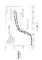
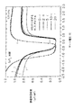
この研究の主な結果を図7−図10にまとめる。図7は、8インチのSiウェハーにおける種々の位置で計測されたAl2O3キャップ層(SiO2等価厚さ数、EOTで表わされる)の厚さへの寄与を示す。EOT数は、キャップされていないケイ酸ハフニウム層の静電容量に対して増加する蓄積静電容量から抽出した。図に示すように、最初の成長抑制の後に、1サイクル当り約0.1nmのAl2O3のリニア成長が観測される。これは、5サイクルより少ない場合にはキャップ層が閉じられそうにないことを示唆するものである。閉鎖されたキャップは、成長速度が厚いAl2O3層と同一であるとき、Al2O3蒸着の10及び20サイクルの後に形成される可能性が高い。
14:ソース/ドレイン拡散領域
16:デバイスチャネル
18:ゲートスタック
20:高k誘電体
22:絶縁中間層
24:Si含有ゲート導体
Claims (24)
- 相補型金属酸化物半導体(CMOS)構造であって、
ソース及びドレイン拡散領域が配置され、該ソース及びドレイン拡散領域がチャネル領域によって分離された半導体基板と、
前記チャネル領域の上に配置されたゲートスタックと、
を備え、前記ゲートスタックは、高kゲート誘電体と、絶縁中間層と、Si含有ゲート導体とからなり、前記絶縁中間層は、前記高kゲート誘電体と前記Si含有ゲート導体との間に配置されて、構造の閾値電圧及びフラットバンド電圧を目標値に安定化させることができる、CMOS構造。 - 前記半導体基板が、Si、Ge、SiGe、SiC、SiGeC、Ga、GaAs、InAs、InP、他のIII/V又はII/VI化合物半導体、有機半導体、又は積層半導体からなる、請求項1に記載のCMOS構造。
- 前記半導体基板が、Si、SiGe、シリコン・オン・絶縁体又はシリコンゲルマニウム・オン・絶縁体からなる、請求項1に記載のCMOS構造。
- 前記半導体基板に、n型ドーパント、p型ドーパント、又はその両方がドープされた、請求項1に記載のCMOS構造。
- 前記高kゲート誘電体が、酸化物、窒化物、酸窒化物又はケイ酸塩からなる、請求項1に記載のCMOS構造。
- 前記高kゲート誘電体が、HfO2、ZrO2、Al2O3、TiO2、La2O3、SrTiO3、LaAlO3、Y2O3、SiO2、窒化SiO2又はケイ酸塩、或いはその窒化物又は窒化ケイ酸塩からなる、請求項1に記載のCMOS構造。
- 前記絶縁中間層が、金属窒化物からなる、請求項1に記載のCMOS構造。
- 前記金属窒化物がさらに酸素を含有する、請求項7に記載のCMOS構造。
- 前記絶縁中間層が、窒化アルミニウム(AlN)、酸窒化アルミニウム(AlOxNy)、窒化ホウ素(BN)、酸窒化ホウ素(BOxNy)、窒化ガリウム(GaN)、酸窒化ガリウム(GaON)、窒化インジウム(InN)、酸窒化インジウム(InON)、又はこれらの組み合わせからなる、請求項1に記載のCMOS構造。
- 前記絶縁中間層がAlN又はAlOxNyからなる、請求項1に記載のCMOS構造。
- 前記絶縁中間層が1から25Åの厚さを有する、請求項1に記載のCMOS構造。
- 前記Si含有ゲート導体がSi又はSiGe合金からなる、請求項1に記載のCMOS構造。
- 前記Si含有ゲート導体が、少なくともホウ素をドープされたポリシリコンからなる、請求項1に記載のCMOS構造。
- 相補型金属酸化物半導体(CMOS)構造であって、
ソース及びドレイン拡散領域が配置され、該ソース及びドレイン拡散領域がチャネル領域によって分離された半導体基板と、
前記チャネル領域の上に配置されたゲートスタックと、
を備え、前記ゲートスタックは、ハフニウム含有高kゲート誘電体と、窒化アルミニウム含有絶縁中間層と、Si含有ゲート導体とからなり、前記窒化アルミニウム絶縁中間層は、前記ハフニウム含有高kゲート誘電体と前記Si含有ゲート導体との間に配置されて、構造の閾値電圧及びフラットバンド電圧を目標値に安定化させることができる、CMOS構造。 - 改善された閾値電圧及びフラットバンド電圧安定性を有する相補型金属酸化物半導体(CMOS)構造を形成する方法であって、
高kゲート誘電体、Si含有ゲート導体、及び前記高kゲート誘電体と前記Si含有ゲート導体との間に配置された絶縁中間層と、からなるゲートスタックを半導体基板上に設けるステップと、
前記ゲートスタックにバイアスをかけて、前記絶縁中間層が構造の閾値電圧及びフラットバンド電圧を目標値に安定化させるようにするステップと、
を含む方法。 - 前記ゲートスタックを設けるステップは、前記高k誘電体、前記絶縁中間層、及び前記Si含有ゲート導体のブランケット層を半導体基板上に蒸着させ、リソグラフィ及びエッチングによって前記ブランケット層にパターン形成することを含む、請求項15に記載の方法。
- 前記ゲートスタックを設けた後に、前記ゲートスタックに当接する前記半導体基板にソース及びドレイン拡散領域が形成される、請求項15に記載の方法。
- 前記絶縁中間層が、蒸着又は熱成長によって形成される、請求項15に記載の方法。
- 前記絶縁中間層が金属窒化物からなる、請求項15に記載の方法。
- 前記金属窒化物がさらに酸素を含有する、請求項19に記載の方法。
- 前記絶縁中間層が、窒化アルミニウム(AlN)、酸窒化アルミニウム(AlOxNy)、窒化ホウ素(BN)、酸窒化ホウ素(BOxNy)、窒化ガリウム(GaN)、酸窒化ガリウム(GaON)、窒化インジウム(InN)、酸窒化インジウム(InON)、又はこれらの組み合わせからなる、請求項15に記載の方法。
- 前記絶縁中間層がAlN又はAlOxNyからなる、請求項15に記載の方法。
- 前記高kゲート誘電体が、HfO2、ケイ酸ハフニウム、又は酸窒化ハフニウムシリコンからなる、請求項15に記載の方法。
- 前記Si含有ゲート導体がSi又はSiGe合金からなる、請求項15に記載の方法。
Applications Claiming Priority (1)
| Application Number | Priority Date | Filing Date | Title |
|---|---|---|---|
| US10/845,719 US20050258491A1 (en) | 2004-05-14 | 2004-05-14 | Threshold and flatband voltage stabilization layer for field effect transistors with high permittivity gate oxides |
Publications (1)
| Publication Number | Publication Date |
|---|---|
| JP2005328059A true JP2005328059A (ja) | 2005-11-24 |
Family
ID=35349796
Family Applications (1)
| Application Number | Title | Priority Date | Filing Date |
|---|---|---|---|
| JP2005139334A Pending JP2005328059A (ja) | 2004-05-14 | 2005-05-12 | 高誘電率ゲート酸化物を有する電界効果トランジスタの閾値及びフラットバンド電圧安定化層 |
Country Status (4)
| Country | Link |
|---|---|
| US (1) | US20050258491A1 (ja) |
| JP (1) | JP2005328059A (ja) |
| CN (1) | CN1697181A (ja) |
| TW (1) | TW200607046A (ja) |
Cited By (11)
| Publication number | Priority date | Publication date | Assignee | Title |
|---|---|---|---|---|
| JP2006086511A (ja) * | 2004-08-17 | 2006-03-30 | Nec Electronics Corp | 半導体装置 |
| WO2008041277A1 (en) | 2006-09-29 | 2008-04-10 | Fujitsu Limited | Compound semiconductor device and process for producing the same |
| JP2008521215A (ja) * | 2004-11-15 | 2008-06-19 | インターナショナル・ビジネス・マシーンズ・コーポレーション | 半導体構造およびそれを形成する方法(金属酸化物の付着を介して形成されたしきい電圧制御層を含む窒素含有電界効果トランジスタ・ゲート・スタック) |
| WO2014069032A1 (ja) * | 2012-11-01 | 2014-05-08 | 独立行政法人産業技術総合研究所 | 電界効果型半導体装置及びその製造方法 |
| KR20150014321A (ko) * | 2013-07-29 | 2015-02-06 | 삼성전자주식회사 | 반도체 소자 및 그 제조 방법 |
| JP2015188116A (ja) * | 2010-12-28 | 2015-10-29 | 株式会社半導体エネルギー研究所 | 半導体装置の作製方法 |
| US9679971B2 (en) | 2015-09-11 | 2017-06-13 | Kabushiki Kaisha Toshiba | Semiconductor device |
| US9755040B2 (en) | 2013-05-31 | 2017-09-05 | Sumitomo Chemical Company, Limited | Semiconductor wafer, method of producing semiconductor wafer and electronic device |
| US9991358B2 (en) | 2015-09-11 | 2018-06-05 | Kabushiki Kaisha Toshiba | Semiconductor device with metal-insulator-semiconductor structure |
| JP2020009884A (ja) * | 2018-07-06 | 2020-01-16 | 国立研究開発法人物質・材料研究機構 | 半導体装置、半導体装置の使用方法およびその半導体装置の製造方法 |
| US10573735B2 (en) | 2017-01-26 | 2020-02-25 | Kabushiki Kaisha Toshiba | Semiconductor device |
Families Citing this family (26)
| Publication number | Priority date | Publication date | Assignee | Title |
|---|---|---|---|---|
| KR100639673B1 (ko) * | 2003-12-22 | 2006-10-30 | 삼성전자주식회사 | 고유전 합금으로 이루어지는 게이트 유전막을 구비하는반도체 소자 및 그 제조 방법 |
| US7105889B2 (en) * | 2004-06-04 | 2006-09-12 | International Business Machines Corporation | Selective implementation of barrier layers to achieve threshold voltage control in CMOS device fabrication with high k dielectrics |
| JP2006216897A (ja) * | 2005-02-07 | 2006-08-17 | Toshiba Corp | 半導体装置及びその製造方法 |
| JP2006278873A (ja) * | 2005-03-30 | 2006-10-12 | Seiko Epson Corp | 半導体装置およびその製造方法 |
| JP2007080995A (ja) * | 2005-09-13 | 2007-03-29 | Toshiba Corp | 半導体装置 |
| TWI262550B (en) * | 2005-10-14 | 2006-09-21 | Ind Tech Res Inst | Element with a low temperature poly-Si film, method of direct poly-Si deposition at low temperature and inductively-coupled plasma chemical vapor deposition |
| US7612421B2 (en) * | 2005-10-11 | 2009-11-03 | Atmel Corporation | Electronic device with dopant diffusion barrier and tunable work function and methods of making same |
| US7655994B2 (en) | 2005-10-26 | 2010-02-02 | International Business Machines Corporation | Low threshold voltage semiconductor device with dual threshold voltage control means |
| US7672093B2 (en) * | 2006-10-17 | 2010-03-02 | Magic Technologies, Inc. | Hafnium doped cap and free layer for MRAM device |
| US8420488B2 (en) | 2007-09-11 | 2013-04-16 | United Microelectronics Corp. | Method of fabricating high voltage device |
| EP2040300B1 (en) * | 2007-09-20 | 2016-07-06 | Imec | MOSFET devices and method to fabricate them |
| JP5208538B2 (ja) * | 2008-02-21 | 2013-06-12 | 株式会社東芝 | 半導体記憶素子 |
| CN101752237B (zh) * | 2008-12-16 | 2012-08-08 | 国际商业机器公司 | 在半导体器件中形成高k栅极叠层的方法 |
| JP5506036B2 (ja) * | 2010-03-02 | 2014-05-28 | 古河電気工業株式会社 | 半導体トランジスタ |
| CN101950757A (zh) * | 2010-07-13 | 2011-01-19 | 中国科学院上海微系统与信息技术研究所 | 基于soi衬底的高介电常数材料栅结构及其制备方法 |
| KR101141244B1 (ko) * | 2010-09-28 | 2012-05-04 | 연세대학교 산학협력단 | 고유전율 물질인 하프늄옥사이드 산화막의 두께 조절을 이용한 게이트 산화막 형성방법 및 이를 이용한 게이트 전극 |
| CN102169104A (zh) * | 2010-12-22 | 2011-08-31 | 重庆邮电大学 | 基于SiC的MOSFET的汽车发动机用氧传感器 |
| CN102776566A (zh) * | 2011-05-11 | 2012-11-14 | 深圳光启高等理工研究院 | 基于多晶硅的超材料制备方法和基于多晶硅的超材料 |
| CN103474340A (zh) * | 2013-09-28 | 2013-12-25 | 复旦大学 | 一种利用双层绝缘层释放费米能级钉扎的方法 |
| CN106158601A (zh) * | 2015-03-26 | 2016-11-23 | 比亚迪股份有限公司 | SiC基器件的栅介质层结构及栅介质层的形成方法 |
| US9859121B2 (en) * | 2015-06-29 | 2018-01-02 | International Business Machines Corporation | Multiple nanosecond laser pulse anneal processes and resultant semiconductor structure |
| EP3353810A4 (en) | 2015-09-25 | 2019-05-01 | Intel Corporation | PASSIVATION OF TRANSISTOR CHANNEL RANGE INTERFACES |
| CN108630700A (zh) * | 2017-03-22 | 2018-10-09 | 中芯国际集成电路制造(上海)有限公司 | 闪存器件及其制造方法 |
| CN108231812A (zh) * | 2018-01-24 | 2018-06-29 | 德淮半导体有限公司 | 晶体管及其制造方法以及cmos图像传感器 |
| DE102019120692B4 (de) * | 2019-07-31 | 2025-12-11 | Infineon Technologies Ag | Leistungshalbleitervorrichtung und Verfahren |
| CN114220865A (zh) * | 2021-12-13 | 2022-03-22 | 深圳市华星光电半导体显示技术有限公司 | 薄膜晶体管及其制作方法、显示面板 |
Citations (6)
| Publication number | Priority date | Publication date | Assignee | Title |
|---|---|---|---|---|
| JP2002246594A (ja) * | 2001-01-08 | 2002-08-30 | Internatl Business Mach Corp <Ibm> | 窒化アルミニウムおよび酸化アルミニウム/窒化アルミニウム・ヘテロ構造ゲート誘電体スタック・ベースの電界効果トランジスタおよびその形成方法 |
| US20020190302A1 (en) * | 2001-06-13 | 2002-12-19 | International Business Machines Corporation | Complementary metal oxide semiconductor (CMOS) gate stack with high dielectric constant gate dielectric and integrated diffusion barrier |
| JP2003282873A (ja) * | 2002-03-22 | 2003-10-03 | Sony Corp | 半導体装置およびその製造方法 |
| JP2004079729A (ja) * | 2002-08-15 | 2004-03-11 | Renesas Technology Corp | 半導体装置 |
| JP2005064317A (ja) * | 2003-08-18 | 2005-03-10 | Semiconductor Leading Edge Technologies Inc | 半導体装置 |
| JP2005210060A (ja) * | 2003-12-26 | 2005-08-04 | Fujitsu Ltd | 半導体装置とその製造方法 |
Family Cites Families (3)
| Publication number | Priority date | Publication date | Assignee | Title |
|---|---|---|---|---|
| US5763922A (en) * | 1997-02-28 | 1998-06-09 | Intel Corporation | CMOS integrated circuit having PMOS and NMOS devices with different gate dielectric layers |
| US6033998A (en) * | 1998-03-09 | 2000-03-07 | Lsi Logic Corporation | Method of forming variable thickness gate dielectrics |
| US6992321B2 (en) * | 2001-07-13 | 2006-01-31 | Motorola, Inc. | Structure and method for fabricating semiconductor structures and devices utilizing piezoelectric materials |
-
2004
- 2004-05-14 US US10/845,719 patent/US20050258491A1/en not_active Abandoned
-
2005
- 2005-05-03 TW TW094114183A patent/TW200607046A/zh unknown
- 2005-05-10 CN CN200510069668.2A patent/CN1697181A/zh active Pending
- 2005-05-12 JP JP2005139334A patent/JP2005328059A/ja active Pending
Patent Citations (6)
| Publication number | Priority date | Publication date | Assignee | Title |
|---|---|---|---|---|
| JP2002246594A (ja) * | 2001-01-08 | 2002-08-30 | Internatl Business Mach Corp <Ibm> | 窒化アルミニウムおよび酸化アルミニウム/窒化アルミニウム・ヘテロ構造ゲート誘電体スタック・ベースの電界効果トランジスタおよびその形成方法 |
| US20020190302A1 (en) * | 2001-06-13 | 2002-12-19 | International Business Machines Corporation | Complementary metal oxide semiconductor (CMOS) gate stack with high dielectric constant gate dielectric and integrated diffusion barrier |
| JP2003282873A (ja) * | 2002-03-22 | 2003-10-03 | Sony Corp | 半導体装置およびその製造方法 |
| JP2004079729A (ja) * | 2002-08-15 | 2004-03-11 | Renesas Technology Corp | 半導体装置 |
| JP2005064317A (ja) * | 2003-08-18 | 2005-03-10 | Semiconductor Leading Edge Technologies Inc | 半導体装置 |
| JP2005210060A (ja) * | 2003-12-26 | 2005-08-04 | Fujitsu Ltd | 半導体装置とその製造方法 |
Cited By (19)
| Publication number | Priority date | Publication date | Assignee | Title |
|---|---|---|---|---|
| JP2006086511A (ja) * | 2004-08-17 | 2006-03-30 | Nec Electronics Corp | 半導体装置 |
| JP2008521215A (ja) * | 2004-11-15 | 2008-06-19 | インターナショナル・ビジネス・マシーンズ・コーポレーション | 半導体構造およびそれを形成する方法(金属酸化物の付着を介して形成されたしきい電圧制御層を含む窒素含有電界効果トランジスタ・ゲート・スタック) |
| WO2008041277A1 (en) | 2006-09-29 | 2008-04-10 | Fujitsu Limited | Compound semiconductor device and process for producing the same |
| US11923249B2 (en) | 2010-12-28 | 2024-03-05 | Semiconductor Energy Laboratory Co., Ltd. | Semiconductor device and method for manufacturing the same |
| JP2015188116A (ja) * | 2010-12-28 | 2015-10-29 | 株式会社半導体エネルギー研究所 | 半導体装置の作製方法 |
| US12288824B2 (en) | 2010-12-28 | 2025-04-29 | Semiconductor Energy Laboratory Co., Ltd. | Semiconductor device including top-gate bottom-contact transistor |
| US10886414B2 (en) | 2010-12-28 | 2021-01-05 | Semiconductor Energy Laboratory Co., Ltd. | Semiconductor device and method for manufacturing the same |
| US10522692B2 (en) | 2010-12-28 | 2019-12-31 | Semiconductor Energy Laboratory Co., Ltd. | Semiconductor device and method for manufacturing the same |
| US11670721B2 (en) | 2010-12-28 | 2023-06-06 | Semiconductor Energy Laboratory Co., Ltd. | Semiconductor device and method for manufacturing the same |
| WO2014069032A1 (ja) * | 2012-11-01 | 2014-05-08 | 独立行政法人産業技術総合研究所 | 電界効果型半導体装置及びその製造方法 |
| US9755040B2 (en) | 2013-05-31 | 2017-09-05 | Sumitomo Chemical Company, Limited | Semiconductor wafer, method of producing semiconductor wafer and electronic device |
| KR20150014321A (ko) * | 2013-07-29 | 2015-02-06 | 삼성전자주식회사 | 반도체 소자 및 그 제조 방법 |
| KR102392059B1 (ko) * | 2013-07-29 | 2022-04-28 | 삼성전자주식회사 | 반도체 소자 및 그 제조 방법 |
| US9991358B2 (en) | 2015-09-11 | 2018-06-05 | Kabushiki Kaisha Toshiba | Semiconductor device with metal-insulator-semiconductor structure |
| US10672882B2 (en) | 2015-09-11 | 2020-06-02 | Kabushiki Kaisha Toshiba | Semiconductor device |
| US10319828B2 (en) | 2015-09-11 | 2019-06-11 | Kabushiki Kaisha Toshiba | Semiconductor device with diffusion prevention layer |
| US9679971B2 (en) | 2015-09-11 | 2017-06-13 | Kabushiki Kaisha Toshiba | Semiconductor device |
| US10573735B2 (en) | 2017-01-26 | 2020-02-25 | Kabushiki Kaisha Toshiba | Semiconductor device |
| JP2020009884A (ja) * | 2018-07-06 | 2020-01-16 | 国立研究開発法人物質・材料研究機構 | 半導体装置、半導体装置の使用方法およびその半導体装置の製造方法 |
Also Published As
| Publication number | Publication date |
|---|---|
| US20050258491A1 (en) | 2005-11-24 |
| CN1697181A (zh) | 2005-11-16 |
| TW200607046A (en) | 2006-02-16 |
Similar Documents
| Publication | Publication Date | Title |
|---|---|---|
| JP2005328059A (ja) | 高誘電率ゲート酸化物を有する電界効果トランジスタの閾値及びフラットバンド電圧安定化層 | |
| US7242055B2 (en) | Nitrogen-containing field effect transistor gate stack containing a threshold voltage control layer formed via deposition of a metal oxide | |
| JP4711444B2 (ja) | 改善されたしきい電圧およびフラットバンド電圧の安定性を有する相補型金属酸化膜半導体(CMOS)構造を形成する方法(高k誘電体によるCMOSデバイス形成におけるしきい電圧制御を達成するためのバリア層の選択的実装) | |
| CN101421839B (zh) | 使用金属/金属氮化物双层结构作为自对准强按比例缩放cmos器件中的栅电极 | |
| US7872317B2 (en) | Dual metal gate self-aligned integration | |
| JP5535706B2 (ja) | 半導体装置の製造方法 | |
| US7884423B2 (en) | Semiconductor device and fabrication method thereof | |
| JP5199104B2 (ja) | 二重の閾値電圧制御手段を有する低閾値電圧の半導体デバイス | |
| JP5270086B2 (ja) | pFET材料としての金属酸窒化物を用いた半導体構造およびその製造方法 | |
| CN101097949A (zh) | 具有栅叠层的半导体结构和制造这种半导体结构的方法 | |
| JP5160238B2 (ja) | n−FET用途のためのHfSiN金属を形成する方法 | |
| US7880241B2 (en) | Low-temperature electrically activated gate electrode and method of fabricating same |
Legal Events
| Date | Code | Title | Description |
|---|---|---|---|
| A621 | Written request for application examination |
Free format text: JAPANESE INTERMEDIATE CODE: A621 Effective date: 20080328 |
|
| RD03 | Notification of appointment of power of attorney |
Free format text: JAPANESE INTERMEDIATE CODE: A7423 Effective date: 20090206 |
|
| A977 | Report on retrieval |
Free format text: JAPANESE INTERMEDIATE CODE: A971007 Effective date: 20111108 |
|
| A131 | Notification of reasons for refusal |
Free format text: JAPANESE INTERMEDIATE CODE: A131 Effective date: 20111129 |
|
| A02 | Decision of refusal |
Free format text: JAPANESE INTERMEDIATE CODE: A02 Effective date: 20120717 |