JP2005347301A - Substrate manufacturing method - Google Patents
Substrate manufacturing method Download PDFInfo
- Publication number
- JP2005347301A JP2005347301A JP2004161565A JP2004161565A JP2005347301A JP 2005347301 A JP2005347301 A JP 2005347301A JP 2004161565 A JP2004161565 A JP 2004161565A JP 2004161565 A JP2004161565 A JP 2004161565A JP 2005347301 A JP2005347301 A JP 2005347301A
- Authority
- JP
- Japan
- Prior art keywords
- substrate
- layer
- manufacturing
- semiconductor
- insulating layer
- Prior art date
- Legal status (The legal status is an assumption and is not a legal conclusion. Google has not performed a legal analysis and makes no representation as to the accuracy of the status listed.)
- Withdrawn
Links
Images

Classifications
-
- H—ELECTRICITY
- H10—SEMICONDUCTOR DEVICES; ELECTRIC SOLID-STATE DEVICES NOT OTHERWISE PROVIDED FOR
- H10P—GENERIC PROCESSES OR APPARATUS FOR THE MANUFACTURE OR TREATMENT OF DEVICES COVERED BY CLASS H10
- H10P90/00—Preparation of wafers not covered by a single main group of this subclass, e.g. wafer reinforcement
- H10P90/19—Preparing inhomogeneous wafers
- H10P90/1904—Preparing vertically inhomogeneous wafers
- H10P90/1906—Preparing SOI wafers
- H10P90/1914—Preparing SOI wafers using bonding
- H10P90/1916—Preparing SOI wafers using bonding with separation or delamination along an ion implanted layer, e.g. Smart-cut
-
- H—ELECTRICITY
- H10—SEMICONDUCTOR DEVICES; ELECTRIC SOLID-STATE DEVICES NOT OTHERWISE PROVIDED FOR
- H10D—INORGANIC ELECTRIC SEMICONDUCTOR DEVICES
- H10D84/00—Integrated devices formed in or on semiconductor substrates that comprise only semiconducting layers, e.g. on Si wafers or on GaAs-on-Si wafers
- H10D84/01—Manufacture or treatment
- H10D84/02—Manufacture or treatment characterised by using material-based technologies
- H10D84/03—Manufacture or treatment characterised by using material-based technologies using Group IV technology, e.g. silicon technology or silicon-carbide [SiC] technology
- H10D84/038—Manufacture or treatment characterised by using material-based technologies using Group IV technology, e.g. silicon technology or silicon-carbide [SiC] technology using silicon technology, e.g. SiGe
-
- H—ELECTRICITY
- H10—SEMICONDUCTOR DEVICES; ELECTRIC SOLID-STATE DEVICES NOT OTHERWISE PROVIDED FOR
- H10D—INORGANIC ELECTRIC SEMICONDUCTOR DEVICES
- H10D88/00—Three-dimensional [3D] integrated devices
- H10D88/01—Manufacture or treatment
-
- H—ELECTRICITY
- H10—SEMICONDUCTOR DEVICES; ELECTRIC SOLID-STATE DEVICES NOT OTHERWISE PROVIDED FOR
- H10P—GENERIC PROCESSES OR APPARATUS FOR THE MANUFACTURE OR TREATMENT OF DEVICES COVERED BY CLASS H10
- H10P50/00—Etching of wafers, substrates or parts of devices
- H10P50/20—Dry etching; Plasma etching; Reactive-ion etching
- H10P50/28—Dry etching; Plasma etching; Reactive-ion etching of insulating materials
- H10P50/282—Dry etching; Plasma etching; Reactive-ion etching of insulating materials of inorganic materials
- H10P50/283—Dry etching; Plasma etching; Reactive-ion etching of insulating materials of inorganic materials by chemical means
-
- H—ELECTRICITY
- H10—SEMICONDUCTOR DEVICES; ELECTRIC SOLID-STATE DEVICES NOT OTHERWISE PROVIDED FOR
- H10P—GENERIC PROCESSES OR APPARATUS FOR THE MANUFACTURE OR TREATMENT OF DEVICES COVERED BY CLASS H10
- H10P90/00—Preparation of wafers not covered by a single main group of this subclass, e.g. wafer reinforcement
- H10P90/19—Preparing inhomogeneous wafers
- H10P90/1904—Preparing vertically inhomogeneous wafers
- H10P90/1906—Preparing SOI wafers
- H10P90/1924—Preparing SOI wafers with separation/delamination along a porous layer
-
- H—ELECTRICITY
- H10—SEMICONDUCTOR DEVICES; ELECTRIC SOLID-STATE DEVICES NOT OTHERWISE PROVIDED FOR
- H10W—GENERIC PACKAGES, INTERCONNECTIONS, CONNECTORS OR OTHER CONSTRUCTIONAL DETAILS OF DEVICES COVERED BY CLASS H10
- H10W10/00—Isolation regions in semiconductor bodies between components of integrated devices
- H10W10/10—Isolation regions comprising dielectric materials
- H10W10/181—Semiconductor-on-insulator [SOI] isolation regions, e.g. buried oxide regions of SOI wafers
Landscapes
- Recrystallisation Techniques (AREA)
- Element Separation (AREA)
Abstract
Description
本発明は、基板の作製方法に関し、特に、側面に絶縁膜が露出されないSOI基板の作製方法に関する。 The present invention relates to a method for manufacturing a substrate, and more particularly to a method for manufacturing an SOI substrate in which an insulating film is not exposed on a side surface.
結合によりSOI基板を作製する方法がいくつか開示されている。代表的な方法として次の3例が挙げられる。 Several methods for fabricating SOI substrates by bonding are disclosed. The following three examples are given as typical methods.
第1の方法は、酸化膜を介して結合した2枚の基板の片側から研削と研磨を行い、酸化膜の上に所望の厚さの基板を残すものである。この技術を基本として、基板を制御良く薄層化する技術がいくつか提案されている。 In the first method, grinding and polishing are performed from one side of two substrates bonded via an oxide film, and a substrate having a desired thickness is left on the oxide film. Based on this technique, several techniques for thinning the substrate with good control have been proposed.
第2の方法は、多孔質Siを用いる技術である(特許文献1参照)。これは、多孔質Si基板上に成長したエピタキシャルSi層を、酸化膜を介してもう一方の支持基板と結合させ、結合強度を高める熱処理を行った後に、前記多孔質Si層内部の応力に沿って外力により劈開分離し、支持基板側に移設された層の表面に残る多孔質Si層を選択的にエッチングして、SOI基板を得る方法(ELTRAN(登録商標))である。また前記方法において、結合した基板の多孔質形成側の裏面から研削を行い、多孔質Si層を露出させた後に多孔質層を選択エッチングしても、同様なSOI基板を得ることができる。 The second method is a technique using porous Si (see Patent Document 1). This is because the epitaxial Si layer grown on the porous Si substrate is bonded to the other supporting substrate through an oxide film, and after heat treatment to increase the bonding strength, the stress inside the porous Si layer is followed. This is a method (ELTRAN (registered trademark)) in which an SOI substrate is obtained by cleaving and separating by external force and selectively etching the porous Si layer remaining on the surface of the layer transferred to the support substrate side. Further, in the above method, a similar SOI substrate can be obtained by grinding from the back side of the bonded substrate on the porous forming side to expose the porous Si layer and then selectively etching the porous layer.
第3の方法は、水素イオン注入を用いる技術である(特許文献2参照)。この方法は2枚のSi基板のうち、少なくとも一方に酸化膜を形成すると共に、一方のSi基板の上面から水素イオン又は希ガスイオンを注入し、該基板内部に微小気泡層(封入層)を形成した後、該イオンを注入した方の面を酸化膜を介して他方のSi基板(支持基板)と密着させ、その後の熱処理により微小気泡層を劈開面として一方の基板を薄膜状に剥離し、更なる熱処理(結合熱処理)を加えて結合強度を高め、SOI基板とする方法(Smart Cut(登録商標)法)である。 The third method is a technique using hydrogen ion implantation (see Patent Document 2). In this method, an oxide film is formed on at least one of two Si substrates, hydrogen ions or rare gas ions are implanted from the upper surface of one Si substrate, and a microbubble layer (encapsulation layer) is formed inside the substrate. After the formation, the surface into which the ions have been implanted is brought into close contact with the other Si substrate (supporting substrate) through an oxide film, and then one substrate is peeled into a thin film by the subsequent heat treatment with the microbubble layer as a cleavage plane. This is a method (Smart Cut (registered trademark) method) in which an additional heat treatment (bonding heat treatment) is applied to increase the bond strength to obtain an SOI substrate.
上記第1〜第3の方法を用いて作製したSOI基板は、最終的に絶縁膜(SiO2)が外周部に露出するという共通の構造を持つ。その結果、半導体デバイスの製造時などにSOI基板の外周部に露出した絶縁膜(SiO2)が選択的にエッチングされて、表層のSi層がテラス状に浮いて強度が弱くなる。これによって、チッピングが生じてSi破片によりウエハ表面が損傷し、高品質な半導体デバイスの歩留まり低下の一要因となることが懸念される。 The SOI substrate manufactured using the first to third methods has a common structure in which an insulating film (SiO 2 ) is finally exposed on the outer peripheral portion. As a result, the insulating film (SiO 2 ) exposed on the outer peripheral portion of the SOI substrate is selectively etched at the time of manufacturing a semiconductor device or the like, and the surface Si layer floats in a terrace shape and the strength is weakened. As a result, there is a concern that chipping occurs and the wafer surface is damaged by Si fragments, which may be a factor in reducing the yield of high-quality semiconductor devices.
そこで、酸化膜の側面がSi単結晶で覆われ、絶縁体がプロセスに悪影響を及ぼすことのないSOI基板が求められている。SOI基板の酸化膜の側面をSi単結晶で覆うためには、表面の中央部に酸化膜を有し且つ表面が平坦である第1の基板を用意し、第2の基板と結合させる必要がある。 Therefore, there is a demand for an SOI substrate in which the side surface of the oxide film is covered with Si single crystal and the insulator does not adversely affect the process. In order to cover the side surface of the oxide film of the SOI substrate with the Si single crystal, it is necessary to prepare a first substrate having an oxide film at the center of the surface and having a flat surface and to bond it to the second substrate. is there.
特許文献3は、Si基板の外周部をSi3N4膜でマスキングし、Si基板の中央部を酸化させた後に、表面を研磨することによって、表面の中央部に酸化膜を有し且つ表面が平坦である第1の基板を作製し、これを第2の基板と結合させてSOI基板を作製する技術を開示している。
しかしながら、特許文献3では、表面の中央部に酸化膜を有し且つ表面が平坦である第1の基板を作製するまでに、基板の全面へSi3N4膜を形成する処理、Si3N4の中央部をエッチングしてマスクを形成する処理、マスクされていない中央部の熱酸化処理、マスク除去処理及び研磨処理と工程数が多く、かつ、複雑な工程を経なければならなかった。 However, in Patent Document 3, a process of forming a Si 3 N 4 film on the entire surface of the substrate before producing a first substrate having an oxide film at the center of the surface and a flat surface, Si 3 N The process of forming a mask by etching the central part of 4 , the thermal oxidation process of the central part not masked, the mask removal process, and the polishing process have a large number of processes and have to undergo complicated processes.
本発明は、上記の問題点に鑑みてなされたものであり、工程数が少なく単純な工程で、側面に絶縁膜が露出されないSOI(Semiconductor On Insulator)基板を作製する方法を提供することを目的とする。 The present invention has been made in view of the above-described problems, and an object of the present invention is to provide a method for manufacturing an SOI (Semiconductor On Insulator) substrate in which an insulating film is not exposed on a side surface in a simple process with a small number of processes. And
本発明は、基板の作製方法に係り、半導体と該半導体の表面に形成された絶縁層とを有する第1の基板を準備する工程と、前記絶縁層の外周部を選択的に除去して前記半導体を露出させる工程と、前記第1の基板の前記絶縁層側と第2の基板とを結合させて結合基板を作製する工程と、を含むことを特徴とする。 The present invention relates to a method for manufacturing a substrate, comprising: preparing a first substrate having a semiconductor and an insulating layer formed on a surface of the semiconductor; and selectively removing an outer peripheral portion of the insulating layer. A step of exposing a semiconductor; and a step of bonding the insulating layer side of the first substrate and a second substrate to form a combined substrate.
本発明によれば、絶縁層の側面が半導体層で覆われるSOI(Semiconductor On Insulator)基板を工程数が少なく単純な工程で実現することができる。 According to the present invention, an SOI (Semiconductor On Insulator) substrate in which a side surface of an insulating layer is covered with a semiconductor layer can be realized by a simple process with a small number of processes.
以下、添付図面を参照して本発明の好適な実施の形態を詳細に説明する。 Preferred embodiments of the present invention will be described below in detail with reference to the accompanying drawings.
[第1の実施形態]
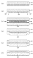
以下、本発明の好適な第1の実施形態に係る基板の作製方法について説明する。図1は、本発明の好適な第1の実施形態に係る基板の作製方法を示す概念図である。
[First embodiment]
A substrate manufacturing method according to the preferred first embodiment of the present invention will be described below. FIG. 1 is a conceptual diagram showing a method for manufacturing a substrate according to a preferred first embodiment of the present invention.
まず、図1(a)に示す工程では、第1の基板101を用意して、その主表面上に絶縁層102を形成する。第1の基板101としては、単結晶Si、多結晶Si、非晶質Si等のSi、Ge、SiGe、SiC、C、GaAs、GaN、AlGaAs、InGaAs、InP、InAs等の半導体が好適である。絶縁層102の絶縁体材料としては、例えば、酸化シリコン、窒化シリコン、酸化窒化シリコン、酸化アルミニウム、酸化タンタル、酸化ハフニウム、酸化チタン、酸化スカンジウム、酸化イットリウム、酸化ガドリニウム、酸化ランタン、酸化ジルコニウム、及びこれらの混合物ガラス等が好適である。絶縁層102は、例えば、第1の基板101の表面を酸化させたり、CVD法又はPVD法により絶縁体物質を堆積させたりすることにより形成され得る。なお、第1の基板101又は第2の基板110が表面に絶縁体を含む場合には、絶縁層102を形成する工程を省略してもよい。
First, in the step shown in FIG. 1A, the
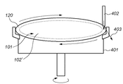
次いで、図1(b)に示す工程では、絶縁層102の外周部120を選択的に除去して第1の基板101を露出させる。絶縁層102の外周部120を選択的に除去する方法としては、例えば、図4〜図6に示す方法が挙げられる。
Next, in the step illustrated in FIG. 1B, the outer
図4は、絶縁層102の外周部120を選択的に除去する第1の方法を模式的に示す図である。第1の基板101は、スピナー401の上に載せられ、所定の回転数で回転する。第1の基板101を回転させると、第1の基板101の外周部120に向けて、ノズル402から酸化膜をエッチングするためのHF等のエッチング液403を供給する。エッチング液403は、遠心力によって第1の基板101の外側に向かって移動するため、第1の基板101の中央部がエッチングされることがない。このようにして、第1の基板101を回転させながら第1の基板101の外周部120をエッチングして、第1の基板101の中央部(外周部120を除く領域)に絶縁層102’を形成することができる。
FIG. 4 is a diagram schematically showing a first method for selectively removing the outer
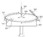
図5は、絶縁層102の外周部120を選択的に除去する第2の方法を模式的に示す図である。第1の基板101は、薬液槽501内のウエハ回転ローラ502上に略垂直に置かれる。ウエハ回転ローラ502には、第1の基板101を支持するための溝が設けられている。ウエハ回転ローラ502を回転させることによって、第1の基板101が回転する。薬液槽501内には、酸化膜をエッチングするためのHF等のエッチング液503が供給される。エッチング液503は、第1の基板101の外周部120がエッチング液503に浸る程度に供給される。
FIG. 5 is a diagram schematically showing a second method for selectively removing the outer
第1の基板101の回転中にエッチング液503が絶縁層102の外周部120以外に回りこむことを防ぐ工夫としては、例えば、以下の2つの方法が考えられる。第1の方法は、第1の基板101と絶縁層102とのエッチング選択比が高い弗化水素等のエッチング液503を用いて、第1の基板101の回転速度を極力遅くするものである(例えば、1時間辺り1回転程度)。絶縁層102を完全にエッチングするので、オーバーエッチングしても問題がない。すなわち、第1の基板101と絶縁層102とのエッチング選択比が高いので、第1の基板101はほとんどエッチングされない。第2の方法は、第1の基板101の表面中央部に純水等のカバーリンスを吹き付けると共に、エッチング液503が薄まらないように薬液槽501にエッチング液503を供給する方法である。この場合、絶縁層102を完全にエッチングするので、エッチング液503の濃度にはほとんど影響しない。
For example, the following two methods are conceivable as means for preventing the
このようにして、第1の基板101の外周部120をエッチング液503に浸して、第1の基板101を回転させることによって、第1の基板101の中央部に絶縁層102’を形成することができる。
In this manner, the outer
図6は、絶縁層102の外周部120を選択的に除去する第3の方法を模式的に示す図である。第1の基板101は、スピナー601の上に載せられ、所定の回転数で回転する。第1の基板101を回転させながら、第1の基板101の外周部120に向けて、ノズル602から酸化膜をエッチングするためのフッ素系ガス等のエッチングガス603を供給すると共に、第1の基板101の中央部に向けて、ノズル604からN2等の不活性ガス605を供給する。第1の基板101の中央部に不活性ガス605を供給しながら第1の基板101の外周部120にエッチングガス603を供給することによって、第1の基板101の中央部がエッチングガス603によってエッチングされることを防止することができる。このようにして、第1の基板101を回転させながら第1の基板101の外周部120をエッチングして、第1の基板101の中央部に絶縁層102’を形成することができる。
FIG. 6 is a diagram schematically showing a third method for selectively removing the outer
なお、絶縁層102の外周部120を選択的に除去する方法は、上記の方法に限定されない。例えば、絶縁層102の中央部(外周部120を除く領域)にマスクを配置し、マスクが配置されていない絶縁層102の外周部120をエッチングすることによって、第1の基板101を露出させてもよい。この場合、エッチングとしては、ウェットエッチング及びドライエッチングの両方を採用することができるが、ウェットエッチングを採用する場合、エッチングが等方的に進行して角度αが90度を超えうるため、より好適であるといえる。第1の基板101の中央部に絶縁層102’を形成した後は、マスクを除去する。このようなマスクの材料としては、例えば、フォトレジストを用いることが好適である。また、薬液やガス等を用いずに、研削等により絶縁層102の外周部120を除去してもよい。
Note that a method for selectively removing the outer
ここで、露出した第1の基板101の表面に対する絶縁層102’の外周側面の角度αが90度以下の角度をなす場合、第1の基板101が変形したとしても、隙間なく結合させることは困難である。したがって、露出した第1の基板101の表面に対する絶縁層102’の外周側面の角度αが90度を超えることが望ましく、より好適には角度αが135度以上であることが望ましい。すなわち、第2の基板110の変形量が少なくて済むので、角度αは180度に近い方が望ましいといえる。
Here, when the angle α of the outer peripheral side surface of the insulating
次いで、図1(c)に示す工程では、第2の基板110を準備する。第2の基板110としては、Si基板、Ge基板、SiGe基板、SiC基板、C基板、GaAs基板、GaN基板、AlGaAs基板、InGaAs基板、InP基板、InAs基板、これらの基板上に絶縁層を形成した基板、石英等の光透過性の基板、サファイヤ等が好適である。しかし、第2の基板20は、結合に供される面が十分に平坦であれば十分であり、他の種類の基板であってもよい。
Next, in the step shown in FIG. 1C, a
次いで、図1(d)に示す工程では、第1の基板101と第2の基板110とを、第2の基板110と絶縁層102’とが面するように室温で密着させて結合基板を作製する。なお、絶縁層102’は、上記のように第1の基板101側に形成しても良いし、第2の基板110側に形成しても良く、両者に形成しても良く、結果として、第1の基板101と第2の基板110とを密着させた際に、図1(d)に示す状態になれば良い。
Next, in the step shown in FIG. 1D, the
第1の基板101の表面では、第1の基板101全体で数μm単位のうねりが生じており、数十〜数nm程度の高低差がある。したがって、第1の基板101の外周部にある程度の段差があっても、第1の基板101表面のうねりや第1の基板101の変形によって段差が吸収されて、隙間無く結合させることができる。第1の基板101の厚さが薄くて変形しやすいほど、そして外周部のSi露出部の結合強度が高いほど、第1の基板101の変形等により吸収される段差は大きくなる。実験的には、約500nm程度の段差が吸収されている。絶縁層102の厚みは薄いほうが望ましいが、本発明はこれに限定されない。
On the surface of the
次いで、図1(e)に示す工程では、第1の基板101と第2の基板110とが完全に密着した後、両者の結合を強固にする処理を実施する。この処理の一例としては、例えば、1)N2雰囲気、1100℃、10minの条件で熱処理を実施し、2)O2/H2雰囲気、1100℃、50〜100minの条件で熱処理(酸化処理)を実施する処理が好適である。
Next, in the step shown in FIG. 1E, after the
次いで、図1(f)に示す工程では、第1の基板101を研削により平坦化する。これにより、絶縁層102’上にシリコン層を有するSOI基板が得られる。
Next, in the step shown in FIG. 1F, the
以上のように、本実施形態によれば、絶縁層を有する第1の基板の絶縁層の外周部を除去し、第1の基板表面を露出させ、絶縁層表面と第1の基板表面に段差(例えば、数百nm)がある状態で結合を行うことによって、側面に絶縁層が露出されないSOI基板を簡単な工程で作製することができる。 As described above, according to the present embodiment, the outer peripheral portion of the insulating layer of the first substrate having the insulating layer is removed, the first substrate surface is exposed, and a step is formed between the insulating layer surface and the first substrate surface. By performing bonding in a state where there is (for example, several hundred nm), an SOI substrate in which the insulating layer is not exposed to the side surface can be manufactured with a simple process.
[第2の実施形態]
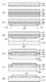
以下、本発明の好適な第2の実施形態に係る基板の作製方法について説明する。図2は、本発明の好適な第2の実施形態に係る基板の作製方法を示す概念図である。
[Second Embodiment]
Hereinafter, a method for manufacturing a substrate according to a preferred second embodiment of the present invention will be described. FIG. 2 is a conceptual diagram showing a method for manufacturing a substrate according to a preferred second embodiment of the present invention.
まず、図2(a)に示す工程では、Si基板201を用意して、その主表面上に分離層としての多孔質Si層202を形成する。多孔質Si層202は、例えば、電解液(化成液)中でSi基板201に陽極化成処理(陽極処理)を施すことによって形成することができる。
First, in the step shown in FIG. 2A, a
ここで、電解液としては、例えば、弗化水素を含む溶液、弗化水素及びエタノールを含む溶液、弗化水素及びイソプロピルアルコールを含む溶液等が好適である。また、多孔質Si層202を互いに多孔度の異なる2層以上の層からなる多層構造としてもよい。ここで、多層構造の多孔質Si層202は、表面側に第1の多孔度を有する第1の多孔質Si層、その下に、第1の多孔度より大きい第2の多孔度を有する第2の多孔質Si層を含むことが好ましい。ここで、第1の多孔度としては、10%〜30%が好ましく、15%〜25%が更に好ましい。また、第2の多孔度としては、35%〜70%が好ましく、40%〜60%が更に好ましい。
Here, as the electrolytic solution, for example, a solution containing hydrogen fluoride, a solution containing hydrogen fluoride and ethanol, a solution containing hydrogen fluoride and isopropyl alcohol, and the like are suitable. The
次いで、図2(b)に示す工程の第1段階では、多孔質Si層202上に第1の非多孔質層203を形成する。第1の非多孔質層203としては、単結晶Si層、多結晶Si層、非晶質Si層等のSi層、Ge層、SiGe層、SiC層、C層、GaAs層、GaN層、AlGaAs層、InGaAs層、InP層、InAs層等が好適である。
Next, in the first stage of the process shown in FIG. 2B, the first
次いで、図2(b)に示す工程の第2段階では、第1の非多孔質層203の上に第2の非多孔質層としての絶縁層204を形成する。絶縁層204の絶縁体材料としては、例えば、酸化シリコン、窒化シリコン、酸化窒化シリコン、酸化アルミニウム、酸化タンタル、酸化ハフニウム、酸化チタン、酸化スカンジウム、酸化イットリウム、酸化ガドリニウム、酸化ランタン、酸化ジルコニウム、及びこれらの混合物ガラス等が好適である。
Next, in the second stage of the process shown in FIG. 2B, an insulating
次いで、図2(c)に示す工程では、図1(b)に示す工程と同様にして、絶縁層204の外周部220をエッチングして、第1の非多孔質層203を露出させる。
Next, in the step shown in FIG. 2C, the outer
次いで、図2(d)に示す工程では、第2の基板210を準備する。第2の基板210としては、Si基板、Ge基板、SiGe基板、SiC基板、C基板、GaAs基板、GaN基板、AlGaAs基板、InGaAs基板、InP基板、InAs基板、これらの基板上に絶縁層を形成した基板、石英等の光透過性の基板、サファイヤ等が好適である。しかし、第2の基板210は、結合に供される面が十分に平坦であれば十分であり、他の種類の基板であってもよい。
Next, in the step shown in FIG. 2D, a
次いで、図2(e)に示す工程の第1段階では、Si基板201と第2の基板210とを、第2の基板210と絶縁層204’とが面するように室温で密着させ、両者の結合を強固にする処理を実施する。この処理は、上述の図1(e)に示す工程と同様にして実施される。
Next, in the first stage of the process shown in FIG. 2E, the
次いで、図2(e)に示す工程の第2段階では、結合基板を機械的強度が脆弱な多孔質層202の部分で分離する。この分離方法としては、各種の方法を採用しうるが、例えば、流体を多孔質層202に打ち込む方法、或いは、流体により多孔質層202に静圧を印加する方法など、流体を利用する方法が好ましい。
Next, in the second stage of the process shown in FIG. 2E, the bonded substrate is separated at the portion of the
この分離工程により、非多孔質層203、絶縁層204’が第2の基板210上に移設される。
By this separation step, the
次いで、図2(f)に示す工程では、分離後の第2の基板210上の多孔質層202’をエッチング等により選択的に除去する。これにより、絶縁層204’上に非多孔質層203を有するSOI基板が得られる。
2F, the porous layer 202 'on the
[第3の実施形態]
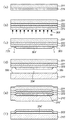
以下、本発明の第3の実施の形態に係る基板の作製方法について説明する。図3は、本発明の好適な第3の実施形態に係る基板の作製方法を示す概念図である。
[Third embodiment]
Hereinafter, a method for manufacturing a substrate according to the third embodiment of the present invention will be described. FIG. 3 is a conceptual diagram showing a method for manufacturing a substrate according to a preferred third embodiment of the present invention.
まず、図3(a)に示す工程では、Si基板301を用意して、その主表面上に絶縁層304を形成する。
First, in the step shown in FIG. 3A, an
次いで、図3(b)に示す工程では、Si基板301に水素イオン306を注入する。水素イオンの加速エネルギーを適当に制御することにより、Si基板301の所定の深さに微小気泡層302が形成される。このとき、Si基板301の表層部分はSi層303となる。
Next, in the step shown in FIG. 3B,
次いで、図3(c)に示す工程では、図1(b)に示す工程と同様にして、絶縁層304の外周部320をエッチングして、第1の非多孔質層303を露出させる。
Next, in the step shown in FIG. 3C, the outer
次いで、図3(d)に示す工程では、第2の基板310を準備する。第2の基板310としては、Si基板、Ge基板、SiGe基板、SiC基板、C基板、GaAs基板、GaN基板、AlGaAs基板、InGaAs基板、InP基板、InAs基板、これらの基板上に絶縁層を形成した基板、石英等の光透過性の基板、サファイヤ等が好適である。しかし、第2の基板310は、結合に供される面が十分に平坦であれば十分であり、他の種類の基板であってもよい。
Next, in the step shown in FIG. 3D, a
次いで、図3(e)に示す工程では、Si基板301と第2の基板310とを、第2の基板310と絶縁層304’とが面するように室温で密着させる。次いで、結合した基板に450〜550℃の熱処理を加えることによって、微小気泡層302が劈開性分離を起こし、結合基板を微小気泡層302の部分で分離する。
Next, in the step shown in FIG. 3E, the
以上のようにして、絶縁層304’上に非多孔質層303を有するSOI基板が得られる(図3(f))。
As described above, an SOI substrate having the
以下、本発明を実施例に基づき説明するが、本発明はこれらの実施例に限定されない。 EXAMPLES Hereinafter, although this invention is demonstrated based on an Example, this invention is not limited to these Examples.
本発明の実施例に係る基板の作製方法を図1に示す。図1は、第1の実施形態に係る基板の作製方法に対応する。 A method for manufacturing a substrate according to an embodiment of the present invention is shown in FIG. FIG. 1 corresponds to the substrate manufacturing method according to the first embodiment.
まず、725μmの厚みを持つSi基板101を用意して、熱酸化を行い、表面に75nmのSiO2層102を形成した(図1(a))。
First, a
次に、図1(b)に示すいずれかの方法を用いて、SiO2膜102の外周部を0.7%フッ化水素酸溶液で10分間エッチングし、外周部5mmにSi基板101の表面が露出する領域を形成した(図1(b))。120は本発明の特徴となる接着領域である。
Next, using one of the methods shown in FIG. 1B, the outer peripheral portion of the SiO 2 film 102 is etched with a 0.7% hydrofluoric acid solution for 10 minutes, and the surface of the
そして、Si基板101のSiO2層102’側とSi基板110とを結合させた(図1(c)、(d))。SiO2層102’による75nmの段差は、Si表面のうねりやSi基板の変形によって吸収され、隙間無く結合することができた。
Then, it was bound to the SiO 2 layer 102 'of the
次いで、1000℃、130分の熱処理を行って、Si基板101のSiO2層102’側とSi基板110とを完全に接着させた(図1(e))。
Next, a heat treatment was performed at 1000 ° C. for 130 minutes to completely bond the
その後、Si基板101側を表面グラインダーを用いて715μm研削した。次いで、コロイダルシリカを砥粒として鏡面研磨を行い、SiO2層102’の上にSi膜101が2μmの厚みで残るようにしてSOIウエハを得た(図1(f))。
Thereafter, the
本発明の実施例に係る基板の作製方法を図2に示す。図2は、第2の実施形態に係る基板の作製方法に対応する。 A method for manufacturing a substrate according to an embodiment of the present invention is shown in FIG. FIG. 2 corresponds to the substrate manufacturing method according to the second embodiment.
Si基板201として、P型(100)の比抵抗0.01ΩcmSi基板を使用し、Si基板201を洗浄した後、陽極化成を行った。陽極化成は49%フッ化水素酸溶液とアルコール溶液を1:1の割合で混合した溶液中で14分間、電流密度10mA/cm2で行った。多孔質化されたSi層202の厚みは15μmであった(図2(a))。
A P-type (100) specific resistance 0.01 Ωcm Si substrate was used as the
次に、酸素雰囲気で400℃、60分間の熱処理を行い多孔質Si層202の表面を安定化させた。その後、多孔質Si層202上にSiをエピタキシャル成長させて、1μmのエピタキシャルSi層203を形成した。エピタキシャル層203の結晶の品質を調べるためにseccoエッチングなどの結晶欠陥の評価を行ったが、欠陥は観察されなかった。
Next, heat treatment was performed at 400 ° C. for 60 minutes in an oxygen atmosphere to stabilize the surface of the
次に、エピタキシャルSi層203を熱酸化して、エピタキシャルSi層203上に75nmのSiO2膜204を形成した(図2(b))。
Next, the
次に、図1(b)に示すいずれかの方法を用いて、SiO2膜204の外周部を0.7%フッ化水素酸溶液で10分間エッチングし、外周部5mmにエピタキシャルSi層203の表面が露出する領域を形成した(図2(c))。220は本発明の特徴となる接着領域である。
Next, using any of the methods shown in FIG. 1B, the outer peripheral portion of the SiO 2 film 204 is etched with a 0.7% hydrofluoric acid solution for 10 minutes, and the
そして、Si基板201のSiO2膜204’側とSi基板210とを結合させた(図2(d))。SiO2層204’による外周部の75nmの段差は、Si表面のうねりやSi基板の変形によって吸収され、隙間無く結合することができた。
Then, the SiO 2 film 204 ′ side of the
次いで、1000℃、130分の熱処理を行って、Si基板201のSiO2膜204’側とSi基板210とを完全に接着させた。その後、ウオータージェットによる流体くさびで多孔質Si層202の部分より2枚のウエハを分離し(図2(e))、多孔質Si層-エピタキシャルSi層−熱酸化膜層-Si基板となる構造をもつ基板を得た(図2(f))。
Next, a heat treatment was performed at 1000 ° C. for 130 minutes to completely bond the
次に、フッ化水素酸溶液と過酸化水素水溶液の混合液を用い、外部から超音波を与えて多孔質Si層202’をエッチングした。この溶液における多孔質Si層202’とエピタキシャルSi層203のエッチング速度差は約10万倍程度であり、エピタキシャルSi層203にダメージを与えることなく多孔質Si層202’をエッチングすることができた。このように、均一なエピタキシャルSi層203を持った、酸化膜が外部に露出されない構造となるSOI半導体を作ることができた(図2(g))。
Next, the
なお、本実施例では、Si基板201を熱酸化してその外周部をエッチングし、Si基板201表面を露出させたものを用いても同様の効果が得られる。また、本実施例では、エピタキシャルSi層203を酸化してSiO2膜204を得たが、Si基板201も熱酸化してその外周部をエッチングしても同様の効果が得られる。
In the present embodiment, the same effect can be obtained even if the
本発明の実施例に係る基板の作製方法を図3に示す。図3は、第3の実施形態に係る基板の作製方法に対応する。 A method for manufacturing a substrate according to an embodiment of the present invention is shown in FIG. FIG. 3 corresponds to the substrate manufacturing method according to the third embodiment.
まず、725μmの厚みを持つSi基板301を用意して、熱酸化を行い、表面に500nmのSiO2層304を形成した(図3(a))。
First, a
この基板の表面から、水素イオン306を注入した。その際に水素イオン306の加速エネルギーを適当に制御することによって、Si基板のある一定の深さに微小気泡層302が形成された。このときSi基板301の表層部分はSi層303となった(図3(b))。
次に、図1(b)に示すいずれかの方法を用いて、SiO2膜304の外周部を0.7%フッ化水素酸溶液で10分間エッチングし、外周部5mmにSi基板301の表面が露出する領域を形成した(図3(c))。320は本発明の特徴となる接着領域である。
Next, using any of the methods shown in FIG. 1B, the outer peripheral portion of the SiO 2 film 304 is etched with a 0.7% hydrofluoric acid solution for 10 minutes, and the surface of the
そして、Si基板301のSiO2層304’側とSi基板310と結合させた(図3(d)、(e))。SiO2層304による75nmの段差は、Si表面のうねりやSi基板の変形によって、吸収され、隙間無く結合することができた。
Then, the
次いで、結合した基板に450〜550℃の熱処理を加えることにより、微小気泡層302から劈開性分離が起こり、支持基板310側がSOI構造となった(図3(f))。
Next, by applying a heat treatment at 450 to 550 ° C. to the bonded substrates, cleavage cleavage occurred from the
なお、実施例1〜3では、SiO2膜をフッ化水素酸溶液を用いてエッチングしたが、研削などにより外周部を除去しても同様の効果が得られる。 In Examples 1 to 3, the SiO 2 film was etched using a hydrofluoric acid solution, but the same effect can be obtained even if the outer peripheral portion is removed by grinding or the like.
101 第1の基板
102、102’ 絶縁層
110 第2の基板
120 絶縁層102の外周部
α 露出した第1の基板101の表面に対する絶縁層102’の外周側面の角度
101 1st board | substrate 102,102 'insulating
Claims (14)
前記絶縁層の外周部を選択的に除去して前記半導体を露出させる工程と、
前記第1の基板の前記絶縁層側と第2の基板とを結合させて結合基板を作製する工程と、
を含むことを特徴とする基板の作製方法。 Providing a first substrate having a semiconductor and an insulating layer formed on the surface of the semiconductor;
Selectively removing the outer periphery of the insulating layer to expose the semiconductor;
Bonding the insulating layer side of the first substrate and a second substrate to produce a combined substrate;
A method for manufacturing a substrate, comprising:
前記第1の基板を回転させながら該第1の基板の外周部にエッチング液を供給する工程を含むことを特徴とする請求項1に記載の基板の作製方法。 Exposing the semiconductor comprises:
The method for manufacturing a substrate according to claim 1, further comprising a step of supplying an etching solution to an outer peripheral portion of the first substrate while rotating the first substrate.
前記第1の基板の外周部をエッチング液に浸す工程と、
前記第1の基板を回転させる工程と、
を含むことを特徴とする請求項1に記載の基板の作製方法。 Exposing the semiconductor comprises:
Immersing the outer periphery of the first substrate in an etchant;
Rotating the first substrate;
The method for manufacturing a substrate according to claim 1, comprising:
前記第1の基板を回転させながら該第1の基板の中央部に不活性ガスを供給すると共に、該第1の基板の外周部にエッチングガスを供給する工程を含むことを特徴とする請求項1に記載の基板の作製方法。 Exposing the semiconductor comprises:
The method includes supplying an inert gas to a central portion of the first substrate while rotating the first substrate and supplying an etching gas to an outer peripheral portion of the first substrate. 2. A method for manufacturing a substrate according to 1.
前記絶縁層の外周部を除く領域にマスクを配置する工程と、
前記マスクが配置されていない前記絶縁層の外周部をエッチングする工程と、
を含むことを特徴とする請求項1に記載の基板の作製方法。 Exposing the semiconductor comprises:
Placing a mask in a region excluding the outer periphery of the insulating layer;
Etching the outer periphery of the insulating layer where the mask is not disposed;
The method for manufacturing a substrate according to claim 1, comprising:
前記分離層の表面に半導体層を形成する工程と、
前記半導体層の表面に絶縁体層を形成する工程と、
を含むことを特徴とする請求項8に記載の基板の作製方法。 Forming the separation layer by making the surface of the semiconductor substrate porous;
Forming a semiconductor layer on the surface of the separation layer;
Forming an insulator layer on a surface of the semiconductor layer;
The method for manufacturing a substrate according to claim 8, comprising:
Priority Applications (2)
| Application Number | Priority Date | Filing Date | Title |
|---|---|---|---|
| JP2004161565A JP2005347301A (en) | 2004-05-31 | 2004-05-31 | Substrate manufacturing method |
| US11/139,484 US20050266657A1 (en) | 2004-05-31 | 2005-05-31 | Substrate manufacturing method |
Applications Claiming Priority (1)
| Application Number | Priority Date | Filing Date | Title |
|---|---|---|---|
| JP2004161565A JP2005347301A (en) | 2004-05-31 | 2004-05-31 | Substrate manufacturing method |
Publications (1)
| Publication Number | Publication Date |
|---|---|
| JP2005347301A true JP2005347301A (en) | 2005-12-15 |
Family
ID=35425918
Family Applications (1)
| Application Number | Title | Priority Date | Filing Date |
|---|---|---|---|
| JP2004161565A Withdrawn JP2005347301A (en) | 2004-05-31 | 2004-05-31 | Substrate manufacturing method |
Country Status (2)
| Country | Link |
|---|---|
| US (1) | US20050266657A1 (en) |
| JP (1) | JP2005347301A (en) |
Families Citing this family (4)
| Publication number | Priority date | Publication date | Assignee | Title |
|---|---|---|---|---|
| TWI270928B (en) * | 2005-07-22 | 2007-01-11 | Sino American Silicon Products | Method of manufacturing composite wafer sructure |
| FR3007576B1 (en) * | 2013-06-19 | 2015-07-10 | Soitec Silicon On Insulator | METHOD OF TRANSFERRING A LAYER OF CIRCUITS. |
| US10276426B2 (en) * | 2016-05-31 | 2019-04-30 | Taiwan Semiconductor Manufacturing Co., Ltd. | System and method for performing spin dry etching |
| CN112467024B (en) * | 2020-11-24 | 2023-04-07 | 上海新硅聚合半导体有限公司 | Preparation method of heterostructure thin film substrate |
Family Cites Families (6)
| Publication number | Priority date | Publication date | Assignee | Title |
|---|---|---|---|---|
| ATE217447T1 (en) * | 1990-08-03 | 2002-05-15 | Canon Kk | METHOD FOR PRODUCING A SEMICONDUCTOR BODY |
| FR2681472B1 (en) * | 1991-09-18 | 1993-10-29 | Commissariat Energie Atomique | PROCESS FOR PRODUCING THIN FILMS OF SEMICONDUCTOR MATERIAL. |
| DE69233314T2 (en) * | 1991-10-11 | 2005-03-24 | Canon K.K. | Process for the production of semiconductor products |
| US5932048A (en) * | 1995-04-06 | 1999-08-03 | Komatsu Electronic Metals Co., Ltd. | Method of fabricating direct-bonded semiconductor wafers |
| US5897333A (en) * | 1997-03-14 | 1999-04-27 | Lucent Technologies, Inc. | Method for forming integrated composite semiconductor devices |
| JP2000186000A (en) * | 1998-12-22 | 2000-07-04 | Speedfam-Ipec Co Ltd | Silicon wafer processing method and apparatus |
-
2004
- 2004-05-31 JP JP2004161565A patent/JP2005347301A/en not_active Withdrawn
-
2005
- 2005-05-31 US US11/139,484 patent/US20050266657A1/en not_active Abandoned
Also Published As
| Publication number | Publication date |
|---|---|
| US20050266657A1 (en) | 2005-12-01 |
Similar Documents
| Publication | Publication Date | Title |
|---|---|---|
| JP4313874B2 (en) | Substrate manufacturing method | |
| US6342433B1 (en) | Composite member its separation method and preparation method of semiconductor substrate by utilization thereof | |
| US6426270B1 (en) | Substrate processing method and method of manufacturing semiconductor substrate | |
| US6376332B1 (en) | Composite member and separating method therefor, bonded substrate stack and separating method therefor, transfer method for transfer layer, and SOI substrate manufacturing method | |
| US7855129B2 (en) | Method for manufacturing direct bonded SOI wafer and direct bonded SOI wafer manufactured by the method | |
| JP3352340B2 (en) | Semiconductor substrate and method of manufacturing the same | |
| JPH09237884A (en) | Method for manufacturing semiconductor substrate | |
| KR20060007428A (en) | Substrate, Method of Manufacturing the Same, and Semiconductor Device | |
| TWI242796B (en) | Substrate and manufacturing method therefor | |
| JP2004103855A (en) | Substrate and method of manufacturing the same | |
| US7368332B2 (en) | SOI substrate manufacturing method | |
| JP2005311199A (en) | Substrate manufacturing method | |
| JP4398934B2 (en) | Manufacturing method of SOI wafer | |
| JPH11288858A (en) | SOI substrate recycling method and recycled substrate | |
| JP3031904B2 (en) | Composite member, method of separating the same, and method of manufacturing semiconductor substrate using the same | |
| JPH10326883A (en) | Substrate and manufacturing method thereof | |
| JP2005347301A (en) | Substrate manufacturing method | |
| JP3013932B2 (en) | Semiconductor member manufacturing method and semiconductor member | |
| JP2004103600A (en) | Substrate and method of manufacturing the same | |
| JP4581349B2 (en) | Manufacturing method of bonded SOI wafer | |
| JP2000188269A (en) | Member separating method and separating apparatus, and substrate manufacturing method | |
| JP2004096044A (en) | Substrate and method of manufacturing the same | |
| JPH1197654A (en) | Semiconductor substrate manufacturing method | |
| JP2004103602A (en) | Substrate and method of manufacturing the same | |
| JP2004103801A (en) | Substrate and method of manufacturing the same |
Legal Events
| Date | Code | Title | Description |
|---|---|---|---|
| A300 | Application deemed to be withdrawn because no request for examination was validly filed |
Free format text: JAPANESE INTERMEDIATE CODE: A300 Effective date: 20070807 |