JP2005347380A - Method and apparatus for manufacturing semiconductor thin film - Google Patents
Method and apparatus for manufacturing semiconductor thin film Download PDFInfo
- Publication number
- JP2005347380A JP2005347380A JP2004162982A JP2004162982A JP2005347380A JP 2005347380 A JP2005347380 A JP 2005347380A JP 2004162982 A JP2004162982 A JP 2004162982A JP 2004162982 A JP2004162982 A JP 2004162982A JP 2005347380 A JP2005347380 A JP 2005347380A
- Authority
- JP
- Japan
- Prior art keywords
- laser light
- thin film
- semiconductor thin
- irradiance
- sub
- Prior art date
- Legal status (The legal status is an assumption and is not a legal conclusion. Google has not performed a legal analysis and makes no representation as to the accuracy of the status listed.)
- Withdrawn
Links
Images


Landscapes
- Thin Film Transistor (AREA)
- Recrystallisation Techniques (AREA)
Abstract
【課題】 安定した特性を有する半導体デバイスを提供するために、幅が広い針状結晶粒を有する半導体薄膜の製造方法を提供する。
【解決手段】 本発明の半導体薄膜の製造方法は、レーザ光の照射により半導体薄膜を溶融し結晶化する方法であって、主レーザ光と、複数の放射照度の異なる副レーザ光を照射し、主レーザ光は、半導体薄膜を溶融する放射照度を有し、副レーザ光は、主レーザ光の放射照度より小さく、半導体薄膜を溶融する放射照度を有し、主レーザ光の照射領域の周囲を照射することを特徴とする。かかる製造方法においては、主レーザ光の照射領域から遠い領域を照射する副レーザ光の放射照度が、主レーザ光の照射領域から近い領域を照射する副レーザ光の放射照度より小さい態様が好ましい。
【選択図】 図1PROBLEM TO BE SOLVED: To provide a method of manufacturing a semiconductor thin film having a wide needle crystal grain in order to provide a semiconductor device having stable characteristics.
A method of manufacturing a semiconductor thin film according to the present invention is a method of melting and crystallizing a semiconductor thin film by laser light irradiation, wherein a main laser light and a plurality of sub laser lights having different irradiances are irradiated, The main laser beam has an irradiance for melting the semiconductor thin film, and the sub laser beam has an irradiance for melting the semiconductor thin film, which is smaller than the irradiance for the main laser beam, and surrounds the irradiation area of the main laser beam. Irradiating. In such a manufacturing method, it is preferable that the irradiance of the sub laser light that irradiates the region far from the main laser light irradiation region is smaller than the irradiance of the sub laser light that irradiates the region close to the main laser light irradiation region.
[Selection] Figure 1
Description
本発明は、レーザ光による加熱で、たとえば、絶縁性基板上に形成された非単結晶半導体薄膜を溶融し、結晶化する半導体薄膜の製造方法および製造装置に関する。 The present invention relates to a semiconductor thin film manufacturing method and a manufacturing apparatus for melting and crystallizing a non-single crystal semiconductor thin film formed on an insulating substrate, for example, by heating with a laser beam.
アモルファス半導体薄膜を結晶化して多結晶半導体薄膜とし、多結晶半導体薄膜にトランジスタを形成した多結晶薄膜トランジスタは、アモルファス半導体薄膜に直接トランジスタを形成したアモルファス薄膜トランジスタに比べて、電界移動度が大きいため、高速動作が期待でき、液晶デバイスの駆動系のみならず、ガラス基板上での大規模集積回路を実現できる可能性を有している。 Polycrystalline thin film transistors in which an amorphous semiconductor thin film is crystallized to form a polycrystalline semiconductor thin film and a transistor is formed on the polycrystalline semiconductor thin film has a higher electric field mobility than an amorphous thin film transistor in which a transistor is formed directly on the amorphous semiconductor thin film. The operation can be expected, and there is a possibility that not only a drive system of a liquid crystal device but also a large-scale integrated circuit on a glass substrate can be realized.
たとえば、画素部分にスイッチング素子を形成するだけでなく、画素周辺部分に駆動回路を形成し、一部の周辺回路を一枚の基板上に形成することができる。このため、別途、ドライバICまたは駆動回路基板を表示装置に実装する必要がなくなるので、表示装置を低価格で提供することが可能となる。 For example, in addition to forming a switching element in the pixel portion, a driver circuit can be formed in the peripheral portion of the pixel, and a part of the peripheral circuit can be formed on a single substrate. For this reason, it is not necessary to separately mount a driver IC or a drive circuit board on the display device, and the display device can be provided at a low price.
また、その他の長所として、トランジスタの寸法を微細化できるので、画素部分に形成するスイッチング素子が小さくなり、高開口率化が図れる。このため、高輝度、高精細な表示装置を提供することが可能となる。 Further, as another advantage, since the size of the transistor can be miniaturized, a switching element formed in the pixel portion can be reduced and a high aperture ratio can be achieved. Therefore, it is possible to provide a display device with high brightness and high definition.
多結晶半導体薄膜は、気相成長法によって得られるアモルファス半導体薄膜を、長時間、ガラスの歪点(約600℃〜650℃)以下で熱アニールするか、レーザなどの高エネルギ密度を有する光を照射する光アニール法によって得られる。光アニール法では、ガラス基板の温度を歪点まで上昇させずに、半導体薄膜のみに高いエネルギを与えることが可能であるため、移動度が高い半導体薄膜の結晶化には非常に有効であると考えられる。 A polycrystalline semiconductor thin film is obtained by thermally annealing an amorphous semiconductor thin film obtained by vapor deposition at a glass strain point (approximately 600 ° C. to 650 ° C.) or lower for a long time, or using light having a high energy density such as a laser. It is obtained by a light annealing method to irradiate. Since the optical annealing method can give high energy only to the semiconductor thin film without raising the temperature of the glass substrate to the strain point, it is very effective for crystallization of a semiconductor thin film with high mobility. Conceivable.
現状では、光アニール法における光源として、エキシマレーザのような大出力パルスレーザが用いられている。線状に整形したエキシマレーザ光をガラス基板上に連続的に照射するエキシマレーザアニーリング法(以下、「ELA法」という。)が一般的である。この方法によって、粒径0.2μm〜0.5μm程度の結晶粒が形成される。このとき、レーザ光を照射した部分のアモルファス半導体は、厚さ方向全域にわたって溶融するのではなく、一部のアモルファス領域を残して溶融することによって、レーザ光照射領域全面にわたって、いたるところに結晶核が発生し、半導体薄膜の最表層に向かって結晶が成長し、ランダムな方位に結晶粒が形成される。 At present, a high-power pulse laser such as an excimer laser is used as a light source in the optical annealing method. An excimer laser annealing method (hereinafter referred to as “ELA method”) in which a glass substrate is continuously irradiated with a linearly shaped excimer laser beam is generally used. By this method, crystal grains having a grain size of about 0.2 μm to 0.5 μm are formed. At this time, the amorphous semiconductor in the portion irradiated with the laser beam is not melted over the entire thickness direction, but is melted while leaving a part of the amorphous region, so that the crystal nuclei are scattered throughout the entire laser beam irradiation region. Occurs, the crystal grows toward the outermost layer of the semiconductor thin film, and crystal grains are formed in random orientations.
さらに高性能な表示装置を得るためには、多結晶シリコンの結晶粒径を大きくすること、結晶の方位を制御することなどが必要であり、単結晶シリコンに近い性能を得ることを目的として数多くの提案がなされている。その中でも特に、結晶を横方向に成長させるラテラル成長法と呼ばれる方法がある(特許文献1参照)。ラテラル成長法は、まず、数μm程度の微細幅のパルスレーザをシリコン薄膜に照射し、シリコン薄膜をレーザ照射領域の厚さ方向全域にわたって溶融し、凝固させて、結晶化を行なう。 In order to obtain a display device with higher performance, it is necessary to increase the crystal grain size of polycrystalline silicon and to control the crystal orientation. Proposals have been made. Among them, there is a method called a lateral growth method in which a crystal is grown in a lateral direction (see Patent Document 1). In the lateral growth method, first, a pulsed laser with a fine width of about several μm is irradiated on a silicon thin film, and the silicon thin film is melted and solidified over the entire thickness direction of the laser irradiation region to perform crystallization.
ラテラル成長法では、溶融部と非溶融部の境界がガラス基板面に対して垂直に形成されるため、そこで発生した結晶核から結晶が全て横方向に成長する。その結果、1パルスのレーザ光照射により、ガラスの基板面に対して平行で、大きさが均一な針状の結晶粒が得られる。1パルスのレーザ光照射により形成される結晶の長さは1μm程度であるが、1回前のレーザ照射で形成された針状結晶の一部に重複するように、順次レーザパルスを照射していくことにより、既に成長した結晶を引継いで、長い針状の結晶粒が得られるという特徴を有する。
矩形状に整形されたレーザ光を半導体薄膜に照射すると、図9に例示するように、溶融部90と非溶融部の界面93に、結晶核が無秩序に発生し、無秩序に発生した多数の結晶核から横方向に結晶が成長するため、針状結晶の幅は不均一となり、非常に幅の狭い結晶粒が形成される。また、両隣の結晶核より横方向に成長した針状結晶に成長を阻害され、結晶幅が狭く、かつ、結晶の長さが短い多数の針状結晶が無秩序に形成される。
When the semiconductor thin film is irradiated with a laser beam shaped in a rectangular shape, as illustrated in FIG. 9, crystal nuclei are generated randomly at the
1回のレーザ光の照射により結晶化した半導体薄膜上に半導体デバイスを作製すると、図10(b)に示すように、大きな針状結晶粒上に半導体デバイス101が形成される場合と、図10(a)に示すように、結晶の幅が狭く、かつ、結晶の長さが短い針状結晶上に半導体デバイス101が形成される場合がある。その結果、半導体デバイス101の特性にバラツキが生じる。これは、図10(a)に示すように、電子の移動方向に結晶粒界が存在するためである。
When a semiconductor device is manufactured on a semiconductor thin film crystallized by one-time laser light irradiation, as shown in FIG. 10B, a
本発明の課題は、安定した特性を有する半導体デバイスを提供するために、幅が広い針状結晶粒を有する半導体薄膜の製造方法を提案することにある。 An object of the present invention is to propose a method for producing a semiconductor thin film having wide needle-like crystal grains in order to provide a semiconductor device having stable characteristics.
本発明の半導体薄膜の製造方法は、レーザ光の照射により半導体薄膜を溶融し結晶化する方法であって、
主レーザ光と、複数の放射照度の異なる副レーザ光を照射し、
主レーザ光は、半導体薄膜を溶融する放射照度を有し、
副レーザ光は、主レーザ光の放射照度より小さく、半導体薄膜を溶融する放射照度を有し、主レーザ光の照射領域の周囲を照射する
ことを特徴とする。
The method for producing a semiconductor thin film of the present invention is a method for melting and crystallizing a semiconductor thin film by laser light irradiation,
Irradiate the main laser beam and multiple sub-laser beams with different irradiance,
The main laser light has an irradiance that melts the semiconductor thin film,
The sub laser light is smaller than the irradiance of the main laser light, has an irradiance for melting the semiconductor thin film, and irradiates around the irradiation region of the main laser light.
かかる製造方法においては、主レーザ光の照射領域から遠い領域を照射する副レーザ光の放射照度が、主レーザ光の照射領域から近い領域を照射する副レーザ光の放射照度より小さい態様が好ましい。また、主レーザ光の照射領域は、副レーザ光の照射領域と一部において重畳し、重畳部の放射照度が他の照射領域の放射照度より小さい態様が好ましい。 In such a manufacturing method, it is preferable that the irradiance of the sub laser light that irradiates the region far from the main laser light irradiation region is smaller than the irradiance of the sub laser light that irradiates the region close to the main laser light irradiation region. Further, it is preferable that the main laser light irradiation region partially overlaps with the sub laser light irradiation region, and the irradiance of the overlapping portion is smaller than the irradiance of other irradiation regions.
主レーザ光の透過部と、副レーザ光の透過部とを有するマスクパターンは、レーザ光の照射により、マスクパターンを半導体薄膜上に結像する態様が望ましい。また、主レーザ光の透過部と、副レーザ光の透過部との間にある遮光部が、半導体薄膜上で解像しない態様が好適である。副レーザ光の透過部の線幅は、主レーザ光の透過部の線幅より小さく、かつ、半導体薄膜上に解像できる線幅より大きくする態様が好ましい。 The mask pattern having the main laser light transmission part and the sub laser light transmission part desirably forms an image on the semiconductor thin film by laser light irradiation. Further, it is preferable that the light shielding portion between the main laser light transmission portion and the sub laser light transmission portion is not resolved on the semiconductor thin film. It is preferable that the line width of the transmission part of the sub laser light is smaller than the line width of the transmission part of the main laser light and larger than the line width that can be resolved on the semiconductor thin film.
本発明の半導体薄膜の製造装置は、レーザ光の照射により半導体薄膜を溶融し結晶化する製造装置であって、
主レーザ光と、複数の放射照度の異なる副レーザ光を照射し、
主レーザ光は、半導体薄膜を溶融する放射照度を有し、
副レーザ光は、主レーザ光の放射照度より小さく、半導体薄膜を溶融する放射照度を有し、主レーザ光の照射領域の周囲を照射する
ことを特徴とする。
The semiconductor thin film manufacturing apparatus of the present invention is a manufacturing apparatus for melting and crystallizing a semiconductor thin film by laser light irradiation,
Irradiate the main laser beam and multiple sub-laser beams with different irradiance,
The main laser light has an irradiance that melts the semiconductor thin film,
The sub laser light is smaller than the irradiance of the main laser light, has an irradiance for melting the semiconductor thin film, and irradiates around the irradiation region of the main laser light.
本発明によれば、ある一定の粒径を有する結晶粒をラテラル成長の結晶核とすることができるため、ラテラル結晶の結晶核の発生密度を抑制し、広い結晶幅をもつ針状結晶粒を有する半導体薄膜を提供することができる。 According to the present invention, since crystal grains having a certain grain size can be used as laterally grown crystal nuclei, the generation density of lateral crystal nuclei is suppressed, and acicular crystal grains having a wide crystal width are formed. A semiconductor thin film can be provided.
(半導体薄膜の製造方法)
本発明の半導体薄膜の製造方法は、レーザ光の照射により半導体薄膜を溶融し、結晶化する方法であって、主レーザ光と、複数の放射照度の異なる副レーザ光を照射し、主レーザ光は、半導体薄膜を溶融する放射照度を有し、副レーザ光は、主レーザ光の放射照度より小さく、半導体薄膜を溶融する放射照度を有し、主レーザ光の照射領域の周囲を照射することを特徴とする。
(Semiconductor thin film manufacturing method)
The method for producing a semiconductor thin film according to the present invention is a method for melting and crystallizing a semiconductor thin film by laser beam irradiation, and irradiating a main laser beam and a plurality of sub-laser beams having different irradiances. Has an irradiance for melting the semiconductor thin film, and the secondary laser light is smaller than the irradiance of the main laser light, has an irradiance for melting the semiconductor thin film, and irradiates around the irradiation area of the main laser light It is characterized by.
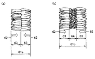
従来から提案されているスーパーラテラル成長法では、図6(a)に示すように、1パルスのレーザ光の照射領域61aにおいて、矢印62の方向に形成される結晶の長さ63は、1μm程度である。また、図6(b)に示すように、結晶のラテラル成長距離61a以上の長さ61bを溶融させた場合でも、溶融領域の中央部64に微細な結晶が形成されるだけであり、より長い針状結晶を形成することはできない。しかし、本発明においては、シリコン薄膜を溶融することができる主レーザ光および副レーザ光からなる第1のレーザ光と、溶融したシリコンの冷却過程を制御することができる第2のレーザ光を用いる溶融結晶化法により、長く、幅の広い針状結晶を形成することができる。
In the conventionally proposed super lateral growth method, as shown in FIG. 6A, the
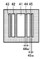
本発明において使用する典型的なマスクを、図4に示す。本明細書においては、第1の開口部41を透過したレーザ光を主レーザ光といい、第2の開口部42を透過したレーザ光と、第3の開口部43を透過したレーザ光と、第4以降の開口部を有するマスクにあっては、第4以降の開口部を透過したレーザ光とを副レーザ光という。また、図3に示すように、第1のレーザ光のほかに、第2のレーザ光を照射する態様においては、主レーザ光および副レーザ光は、第1のレーザ光に関するものをいう。
A typical mask used in the present invention is shown in FIG. In this specification, the laser light transmitted through the
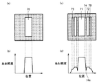
従来技術において、第1のレーザ光を整形するマスクは、図7(a)に示すように、単一の開口部76を有するものであり、その場合のレーザ光は、図7(b)に示すような放射照度分布を示す。このようなレーザ光を照射すると、溶融部と非溶融部との界面に、結晶核が無秩序に発生する。そのため、無秩序に発生した多数の結晶核から横方向に結晶が成長し、図9に示すように、針状結晶の幅は不均一となり、非常に幅の狭い結晶粒が形成される。
In the prior art, the mask for shaping the first laser beam has a
また、両隣りの結晶核から横方向に成長した針状結晶により、成長が阻害され、結晶幅が狭く、かつ、結晶の長さが短い多数の針状結晶が無秩序に形成される。特に、飛躍的に長い針状結晶が形成される場合には、結晶粒ごとの結晶の幅および結晶の長さの違いが顕著に現れる。 In addition, the needle-like crystals grown laterally from the adjacent crystal nuclei inhibit growth, and a large number of needle-like crystals with a narrow crystal width and a short crystal length are formed randomly. In particular, when a drastically long needle-like crystal is formed, the difference in crystal width and crystal length for each crystal grain appears significantly.
このため、1回のレーザ光の照射により結晶化した半導体薄膜上に、半導体デバイスを作製すると、図10(b)に示すような、大きな針状結晶粒上に半導体デバイス101が形成される場合と、図10(a)に示すような、結晶の幅が狭く、かつ、結晶の長さが短い針状結晶上に半導体デバイス101が形成される場合があり、その結果、半導体デバイスの特性にバラツキが生じる。
Therefore, when a semiconductor device is formed on a semiconductor thin film that has been crystallized by a single laser beam irradiation, the
本発明において使用する典型的なマスクを、図7(c)に示す。かかるマスクにより整形される第1のレーザ光の放射照度分布を、図7(d)に示す。図7(d)に示すように、本発明のレーザ光は、半導体薄膜上において、第1の遮光部74により、放射照度分布に凹部、すなわち、暗部74aが形成される。また、第1の開口部71を透過するレーザ光の放射照度より、第2の開口部72および第3の開口部73をそれぞれ透過するレーザ光の放射照度の方が小さくなるように調整する。
A typical mask used in the present invention is shown in FIG. The irradiance distribution of the first laser beam shaped by such a mask is shown in FIG. As shown in FIG. 7D, in the laser light of the present invention, a concave portion, that is, a
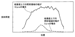
調整は、第2の開口部72および第3の開口部73の線幅を、第1の開口部71の線幅より狭くすることにより行なうことができる。図8に、レーザ光の結像面上での照射領域(スリット)の幅と放射照度との関係を示す。図8に示すように、結像面における照射領域の幅が3μmの場合の放射照度は、照射領域の幅が10μmの場合の放射照度と比較して小さくなる。したがって、矩形マスクの開口部の線幅が狭い程、放射照度のピーク部(最明部)が小さくなる。
The adjustment can be performed by making the line widths of the
マスクの開口部を透過したレーザ光を集光する結像レンズのMTF(Modulus Transfer Function)は、一般に、空間周波数が大きい程、小さくなる。たとえば、マスクにおける開口部の線幅が10μmである場合の空間周波数は、1/(0.01×2)=50(本/mm)であり、開口部の線幅が2μmである場合の空間周波数は、1/(0.002×2)=250(本/mm)であり、また、開口部の線幅が1μmである場合の空間周波数は、1/(0.001×2)=500(本/mm)である。MTFは、像のコントラストを示しているので、マスクパターンの開口部の線幅を調整することにより、放射照度を任意に調整することができる。たとえば、開口部の線幅が広いと、空間周波数が小さく、MTFは大きくなって、放射照度を高めることができる。 In general, the MTF (Modulus Transfer Function) of the imaging lens that condenses the laser light transmitted through the opening of the mask decreases as the spatial frequency increases. For example, the spatial frequency when the line width of the opening in the mask is 10 μm is 1 / (0.01 × 2) = 50 (lines / mm), and the space when the line width of the opening is 2 μm. The frequency is 1 / (0.002 × 2) = 250 (lines / mm), and the spatial frequency when the line width of the opening is 1 μm is 1 / (0.001 × 2) = 500. (Books / mm). Since the MTF indicates the contrast of the image, the irradiance can be arbitrarily adjusted by adjusting the line width of the opening of the mask pattern. For example, if the line width of the opening is wide, the spatial frequency is small, the MTF is large, and the irradiance can be increased.
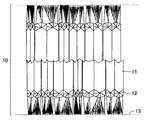
本発明における結晶化処理について、図1を用いて説明する。レーザ光による溶融後、まず、溶融部10と非溶融部の界面13に多数の結晶核が形成される。つづいて、マスク上の第1の遮光部に相当する位置において、結晶核12が形成される。第1の遮光部に相当する位置に形成された結晶核12は、溶融部10と非溶融部の界面13に形成される結晶核とは異なり、周囲が加熱されているため、大きな結晶粒となる。さらに、マスク上の第1の開口部から第1の遮光部に相当する位置において、温度勾配があるため、第1の遮光部に相当する位置に形成された結晶核12を種結晶として、第1の開口部を透過する主レーザの照射領域に、ラテラル成長する長い結晶11が形成される。
The crystallization treatment in the present invention will be described with reference to FIG. After melting by laser light, first, a large number of crystal nuclei are formed at the
従来から提案されているスーパーラテラル成長法において、単一の開口部を有する従来のマスクを用いる場合、ラテラル成長は、溶融部と非溶融部との界面において形成される結晶核より開始する。それに対して、本発明では、第1の遮光部に相当する位置において形成された大きな結晶粒が種結晶となり、ラテラル成長はその大きな種結晶より開始する。このため、大きな種結晶の結晶幅を引継いで横方向成長し、図1に示すように、主レーザ光の照射領域には、幅の広い結晶粒を得ることができる。 In a conventionally proposed super lateral growth method, when a conventional mask having a single opening is used, the lateral growth starts from a crystal nucleus formed at the interface between the melted part and the non-melted part. On the other hand, in the present invention, large crystal grains formed at a position corresponding to the first light shielding portion become seed crystals, and lateral growth starts from the large seed crystals. For this reason, the crystal width of the large seed crystal is taken over and laterally grown, and as shown in FIG. 1, wide crystal grains can be obtained in the main laser light irradiation region.
本発明の製造方法においては、レーザ光の照射により半導体薄膜を溶融し、結晶化する。したがって、主レーザ光と副レーザ光は、半導体薄膜を溶融する放射照度を有する。また、結晶化工程において、まず、溶融部と非溶融部との界面に結晶核を形成し、つぎに、主レーザ光の透過部と副レーザ光の透過部との間にある第1の遮光部に相当する位置に結晶核を形成し、最後に、主レーザ光の照射領域に、針状結晶を成長させる。このため、放射照度の低い副レーザ光を、放射照度の高い主レーザ光の周囲に照射し、また、放射照度の異なる複数の副レーザ光を照射して、加熱を調整する。かかる構成により、幅1μm以上の結晶を得ることができる。 In the manufacturing method of the present invention, the semiconductor thin film is melted and crystallized by laser light irradiation. Therefore, the main laser light and the sub laser light have irradiance for melting the semiconductor thin film. In the crystallization step, first, crystal nuclei are formed at the interface between the melted part and the non-melted part, and then the first light shielding between the main laser light transmission part and the sub laser light transmission part. A crystal nucleus is formed at a position corresponding to the portion, and finally a needle crystal is grown in the irradiation region of the main laser beam. For this reason, the sub laser light with low irradiance is irradiated around the main laser light with high irradiance, and a plurality of sub laser lights with different irradiance are irradiated to adjust the heating. With this configuration, a crystal having a width of 1 μm or more can be obtained.
主レーザ光の照射領域から遠い領域を照射する副レーザ光の放射照度を、主レーザ光の照射領域から近い領域を照射する副レーザ光の放射照度より小さくすることにより、溶融後の結晶化工程において、まず、溶融部と非溶融部との界面に結晶核を形成し、つづいて、第1の遮光部に相当する位置に形成する結晶核の周囲を加熱して、大きな結晶核とし、大きな結晶核を種結晶として、幅が広い結晶をラテラル成長させることができる。 Crystallization process after melting by making the irradiance of the sub laser light irradiating the area far from the main laser light irradiation area smaller than the irradiance of the sub laser light irradiating the area near the main laser light irradiation area First, a crystal nucleus is formed at the interface between the melted part and the non-melted part, and then the periphery of the crystal nucleus formed at a position corresponding to the first light shielding part is heated to form a large crystal nucleus. With a crystal nucleus as a seed crystal, a wide crystal can be laterally grown.
副レーザ光は、主レーザ光の照射領域の周囲を照射する。副レーザ光を、主レーザ光の照射領域の周囲に照射するとは、図7(c)と図7(d)において、第2の開口部72を透過する副レーザ光が、主レーザ光の照射領域の外縁部を照射する場合のように、副レーザ光の照射領域と主レーザ光の照射領域が重畳する態様が含まれる。また、第3の開口部73を透過する副レーザ光が主レーザ光の照射領域の外回りを照射する場合のように、副レーザ光の照射領域と主レーザ光の照射領域が重畳する部分を有しない態様が含まれる。
The sub laser light irradiates around the irradiation area of the main laser light. The sub laser light is irradiated around the irradiation region of the main laser light. In FIGS. 7C and 7D, the sub laser light transmitted through the
第1の遮光部に相当する位置において、主レーザ光の照射領域と、副レーザ光の照射領域が重畳し、重畳部の放射照度が他の照射領域の放射照度より小さい態様が好ましい。かかる態様により、第1の遮光部に相当する位置において、大径の結晶核を形成することができる。同様に、主レーザ光の透過部と、副レーザ光の透過部との間にある第1の遮光部が半導体薄膜上に解像しない態様とすることにより、第1の遮光部に相当する位置における結晶核の形成を促進することができる。 It is preferable that the main laser light irradiation region and the sub laser light irradiation region overlap at a position corresponding to the first light shielding portion, and the irradiance of the overlapping portion is smaller than the irradiance of other irradiation regions. According to such an embodiment, a large-diameter crystal nucleus can be formed at a position corresponding to the first light shielding portion. Similarly, a position corresponding to the first light-shielding portion is obtained by adopting an aspect in which the first light-shielding portion between the main laser light transmission portion and the sub-laser light transmission portion is not resolved on the semiconductor thin film. The formation of crystal nuclei in can be promoted.
主レーザ光の透過部と、副レーザ光の透過部とを有するマスクパターンに、レーザ光を照射して、マスクパターンを半導体薄膜上に結像する態様は、主レーザ光と副レーザ光により半導体薄膜を効率的に加熱する上で好ましい。また、副レーザ光の放射照度を、主レーザ光の放射照度より小さくする点で、副レーザ光の透過部の線幅は、主レーザ光の透過部の線幅より小さくするのが好ましい。しかし、副レーザ光により効率的に加熱するため、副レーザ光の透過部の線幅は、半導体薄膜上に解像できる線幅より大きい態様が好ましい。 The mask pattern having the main laser light transmission part and the sub laser light transmission part is irradiated with laser light to form an image on the semiconductor thin film. It is preferable for efficiently heating the thin film. Moreover, it is preferable that the line width of the transmission part of the sub laser light is made smaller than the line width of the transmission part of the main laser light in that the irradiance of the sub laser light is made smaller than that of the main laser light. However, in order to efficiently heat with the sub laser light, it is preferable that the line width of the transmission part of the sub laser light is larger than the line width that can be resolved on the semiconductor thin film.
一方、エキシマレーザのフルエンスが大きい場合、第1の遮光部の幅が狭い場合、第3の開口部が無い場合は、溶融部と非溶融部との界面で多数形成される結晶核を起点として、横方向に成長した結晶が、第1の遮光部に相当する位置に別の結晶核が形成される前に、第1の遮光部に相当する位置に到達しやすくなる。そのため、従来の単一の開口部を有するマスクパターンを用いた場合と同様の結晶化組織となりやすい。 On the other hand, when the fluence of the excimer laser is large, when the width of the first light shielding portion is narrow, or when there is no third opening, the crystal nucleus formed at the interface between the melted portion and the non-melted portion is the starting point. The crystals grown in the lateral direction are likely to reach a position corresponding to the first light shielding portion before another crystal nucleus is formed at a position corresponding to the first light shielding portion. Therefore, it tends to have a crystallized structure similar to that when a conventional mask pattern having a single opening is used.
また、エキシマレーザのフルエンスが小さい場合、第1の遮光部の幅が広い場合は、第1の遮光部に相当する位置に形成される結晶核の大きさが小さくなりやすいため、大きな結晶幅を有する針状結晶を形成しにくくなる。 In addition, when the fluence of the excimer laser is small, when the width of the first light shielding portion is wide, the size of the crystal nucleus formed at the position corresponding to the first light shielding portion is likely to be small. It becomes difficult to form the acicular crystals.
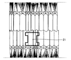
よって、本発明におけるマスクパターンは、所望する結晶長が形成されるレーザ光照射条件に合わせて、第2の開口部、第3開口部、第1の遮光部および第2の遮光部のそれぞれの幅を設定するのが好ましい。また、本発明における開口部の数も3個に限定されるものではなく、第4の開口部など任意に設定することが可能である。本発明により、図2に示すように安定した特性を有する半導体デバイス21を提供することが可能となる。
Therefore, the mask pattern according to the present invention has the second opening, the third opening, the first light-shielding part, and the second light-shielding part in accordance with the laser beam irradiation conditions for forming a desired crystal length. It is preferable to set the width. Further, the number of openings in the present invention is not limited to three, and can be arbitrarily set such as a fourth opening. According to the present invention, it is possible to provide a
(半導体薄膜の製造装置)
本発明の半導体薄膜の製造装置は、レーザ光の照射により半導体薄膜を溶融し、結晶化する製造装置であって、主レーザ光と、複数の放射照度の異なる副レーザ光を照射し、主レーザ光は、半導体薄膜を溶融する放射照度を有し、副レーザ光は、主レーザ光の放射照度より小さく、半導体薄膜を溶融する放射照度を有し、主レーザ光の照射領域の周囲を照射することを特徴とする。かかる製造装置により、幅が広く、長い結晶を有する半導体薄膜を製造することができる。
(Semiconductor thin film manufacturing equipment)
The semiconductor thin film manufacturing apparatus of the present invention is a manufacturing apparatus that melts and crystallizes a semiconductor thin film by laser beam irradiation, and irradiates a main laser beam and a plurality of sub laser beams having different irradiances. The light has an irradiance for melting the semiconductor thin film, and the sub laser light has an irradiance for melting the semiconductor thin film, which is smaller than the irradiance of the main laser light, and irradiates around the irradiation area of the main laser light. It is characterized by that. With such a manufacturing apparatus, a semiconductor thin film having a wide crystal and a long crystal can be manufactured.
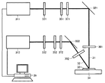
本発明の半導体薄膜の製造装置の具体例を図3に示す。図3に示すように、この製造装置は、第1のレーザ光発振器311、第2のレーザ光発振器312、アッテネータ331、332、均一照射光学系351、352、マスク371、372、半導体基板33をXY方向に所定の速度で移動できるステージ34、結像レンズ301、302、ミラー321、322および制御装置35を備える。
A specific example of the semiconductor thin film manufacturing apparatus of the present invention is shown in FIG. As shown in FIG. 3, this manufacturing apparatus includes a first
第1のレーザ光発振器311は、パルス状のエネルギビームを照射し、半導体膜を溶融することが可能であれば、特に限定されるものでなく、たとえば、エキシマレーザ、YAGレーザに代表される各種固体レーザなどを用いることができる。また、紫外域の波長を有する光源が望ましく、たとえば、波長308nmのエキシマレーザを好ましく用いることができる。第1のレーザのフルエンスは、3000〜5000J/m2(300〜500mJ/cm2)が好適である。
The first
第2のレーザ光発振器312には、レーザ光を連続照射するもの、または、パルス照射するものなどを用いることができるが、溶融シリコンに吸収されるレーザ光を発振するものが好ましい。たとえば、波長532nmのYAGレーザ、波長1064nmのYAGレーザ、波長10.6μmのCO2レーザを好ましく用いることができる。
As the second
アッテネータ331、332は、第1のレーザ光発振器311および第2のレーザ光発振器312から照射されたレーザをそれぞれ所定の光量に減衰させ、放射照度を調整する機能を有する。
The
均一照射光学系351、352は、レーザ光発振器から照射したレーザ光の放射照度分布を均一化する機能を有する。
The uniform irradiation
結像レンズ301は、半導体薄膜上に、マスク371の開口部を透過した第1のレーザ光31を所定の倍率で結像させる機能を有する。この像は、マスクパターンと相似形となる。同様に、結像レンズ302は、半導体薄膜上に、マスク372の開口部を透過した第2のレーザ光32を所定の倍率で結像させる機能を有する。この像は、マスクパターンと相似形となる。
The
ミラー321、322は、レーザ光を折返すために用いるが、配置箇所および数量に制限はなく、装置の光学設計および機構設計に応じて、適切に配置することが可能である。
The
制御装置35は、第1のレーザ光と第2のレーザ光の照射のタイミングを制御する機能を有する。また、制御装置35は、ステージ34の位置制御、レーザ光照射目標位置の記憶、装置内部の温度制御および装置内部の雰囲気などを制御する機能を有する。
The
マスク371、372は、レーザ光が透過する開口部(透過部)と、レーザ光が透過しない遮光部とからなり、均一照射光学系351、352によって、放射照度分布が均一化されたレーザ光の一部を開口部によって透過し、遮光部によって遮光する機能を有する。
The
マスクの開口部の形状であるマスクパターンは、たとえば、図4に示すように、矩形の第1の開口部(第1の透過部)41と、第1の開口部41の周辺に、第2の開口部42と、第3の開口部43とを有する。第1の開口部41と第2の開口部42の間には、第1の遮光部44が形成されている。また、第2の開口部42と第3の開口部43の間には、第2の遮光部45が形成されている。
For example, as shown in FIG. 4, the mask pattern which is the shape of the opening of the mask has a rectangular first opening (first transmitting portion) 41 and the second opening around the
第2の開口部42と第3の開口部43とは、いずれも、レーザ加工装置の光学系が有する解像線幅以上の幅があり、また、いずれも、第1の開口部41の幅より狭いものが好ましい。一方、第1の遮光部44と第2の遮光部45とは、レーザ加工装置の光学系が有する解像線幅以下の幅を有するものが好ましい。マスクパターンの具体的な寸法は、レーザ光照射条件に合わせて任意に設定することが可能であり、第1の開口部の幅は、形成したい結晶の長さの2倍程度が好ましい。
Each of the
マスクパターンを、結像レンズ301、302を用いて基板上に結像させるが、レンズは回折限界光学系であることから、解像度には限界がある。解像の限界幅である解像線幅Rは、光の波長λ、レンズの開口率NAおよび定数kにより、
R=k×λ/NA
と表すことができる。
The mask pattern is imaged on the substrate using the
R = k × λ / NA
It can be expressed as.
たとえば、解像線幅Rが1.0μmである光学系を用いる場合、図4において、第1の遮光部44の線幅44wと、第2の遮光部45の線幅45wとを、少なくとも1.0μm未満とすると、遮光部は半導体薄膜上に解像しなくなる。
For example, when an optical system having a resolution line width R of 1.0 μm is used, the
実施例1
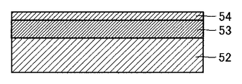
本実施例で用いた具体的な半導体基板の膜構造を図5に示す。図5に示すとおり、厚さ0.7mmのガラス基板52上に、厚さ100nmの酸化珪素膜(SiO2)53と、厚さ50nmの非晶質珪素膜(a−Si)54を、CVD(Chemical Vapor Deposition)法により形成した。
Example 1
FIG. 5 shows a specific film structure of the semiconductor substrate used in this example. As shown in FIG. 5, a 100 nm thick silicon oxide film (SiO 2 ) 53 and a 50 nm thick amorphous silicon film (a-Si) 54 are formed on a 0.7 mm
つぎに、本実施例におけるレーザ光照射方法について説明する。図3に示すように、第1のレーザ光発振器311は、波長308nmのレーザ光を照射するエキシマレーザを用い、第1のレーザ光のフルエンスは3500J/m2(350mJ/cm2)とした結果、第1のレーザ光の照射により半導体薄膜は溶融した。
Next, a laser beam irradiation method in this embodiment will be described. As shown in FIG. 3, the first
第1のレーザ光に使用したマスクパターンは、図4に示すように、第1の開口部41と、第1の開口部41の周囲に、第2の開口部42と第3の開口部43を形成したものを用いた。このため、第2の開口部42と第3の開口部43を透過する副レーザ光は、第1の開口部41を透過する主レーザ光の照射領域の周囲を照射した。また、開口部の寸法は、結像面上で、第1の開口部41の線幅を10μm、第2の開口部42の線幅を2μm、第3の開口部43の線幅を1μmとした。このため、図8の実験結果からも明らかなとおり、主レーザ光と、複数の放射照度の異なる副レーザ光を照射し、副レーザ光は主レーザ光の放射照度より小さくなった。また、主レーザ光および副レーザ光はともに、半導体薄膜を溶融し得る放射照度を有していた。
As shown in FIG. 4, the mask pattern used for the first laser light has a
マスクにおける第1の遮光部44の線幅は、結像面上で、0.5μm、第2の遮光部45の線幅は0.25μmした。第1のレーザ光については、解像線幅が1.0μmの光学系を用いたため、遮光部44,45は、解像しなかった。結像レンズ301の倍率は1/4とした。
The line width of the first
第2のレーザ光発振器312は、波長10.6μmのレーザ光を照射するCO2レーザを用いた。第2のレーザ光32のパルス幅は120μsec、フルエンスは8500J/m2とした。第2のレーザ光32は、基板33上におけるサイズが5.5mm×5.5mmの矩形状に整形した。
The second
図3に示すように、半導体基板33上には、まず、第2のレーザ光を照射した後、第1のレーザ光を照射した。半導体基板33に、第1のレーザ光31を垂直方向から入射し、第2のレーザ光32を斜め方向から入射した。
As shown in FIG. 3, the
レーザ光の照射により半導体薄膜は溶融し、結晶化して、図1に示すような結晶構造が得られた。結晶11のサイズは、長さが5μm、幅が1μmであった。つぎに、図2に示すように、針状結晶上に半導体デバイスを形成すると、電子の移動方向に結晶粒界がないため、安定した特性を有する半導体デバイスを製造することができた。
The semiconductor thin film was melted and crystallized by laser light irradiation, and a crystal structure as shown in FIG. 1 was obtained. The
今回開示された実施の形態および実施例はすべての点で例示であって制限的なものではないと考えられるべきである。本発明の範囲は上記した説明ではなくて特許請求の範囲によって示され、特許請求の範囲と均等の意味および範囲内でのすべての変更が含まれることが意図される。 It should be understood that the embodiments and examples disclosed herein are illustrative and non-restrictive in every respect. The scope of the present invention is defined by the terms of the claims, rather than the description above, and is intended to include any modifications within the scope and meaning equivalent to the terms of the claims.
本発明によれば、安定した特性を有する半導体デバイスを提供することができる。 According to the present invention, a semiconductor device having stable characteristics can be provided.
10 溶融部、11 結晶、12 結晶核、13 溶融部と非溶融部の界面、21 半導体デバイス、41 第1の開口部、42 第2の開口部、43 第3の開口部、44 第1の遮光部、45 第2の遮光部。 10 melting part, 11 crystal, 12 crystal nucleus, 13 interface between melting part and non-melting part, 21 semiconductor device, 41 first opening part, 42 second opening part, 43 third opening part, 44 first part Light shielding part, 45 Second light shielding part.
Claims (7)
主レーザ光と、複数の放射照度の異なる副レーザ光を照射し、
主レーザ光は、半導体薄膜を溶融する放射照度を有し、
副レーザ光は、主レーザ光の放射照度より小さく、半導体薄膜を溶融する放射照度を有し、主レーザ光の照射領域の周囲を照射する
ことを特徴とする半導体薄膜の製造方法。 A method of melting and crystallizing a semiconductor thin film by laser light irradiation,
Irradiate the main laser beam and multiple sub-laser beams with different irradiance,
The main laser light has an irradiance that melts the semiconductor thin film,
A method for producing a semiconductor thin film, wherein the sub laser light has an irradiance for melting the semiconductor thin film, which is smaller than the irradiance of the main laser light, and irradiates the periphery of the irradiation region of the main laser light.
主レーザ光と、複数の放射照度の異なる副レーザ光を照射し、
主レーザ光は、半導体薄膜を溶融する放射照度を有し、
副レーザ光は、主レーザ光の放射照度より小さく、半導体薄膜を溶融する放射照度を有し、主レーザ光の照射領域の周囲を照射する
ことを特徴とする半導体薄膜の製造装置。 A manufacturing apparatus for melting and crystallizing a semiconductor thin film by laser irradiation,
Irradiate the main laser beam and multiple sub-laser beams with different irradiance,
The main laser light has an irradiance that melts the semiconductor thin film,
The sub-laser light has an irradiance for melting the semiconductor thin film, which is smaller than the irradiance of the main laser light, and irradiates the periphery of the irradiation region of the main laser light.
Priority Applications (1)
| Application Number | Priority Date | Filing Date | Title |
|---|---|---|---|
| JP2004162982A JP2005347380A (en) | 2004-06-01 | 2004-06-01 | Method and apparatus for manufacturing semiconductor thin film |
Applications Claiming Priority (1)
| Application Number | Priority Date | Filing Date | Title |
|---|---|---|---|
| JP2004162982A JP2005347380A (en) | 2004-06-01 | 2004-06-01 | Method and apparatus for manufacturing semiconductor thin film |
Publications (1)
| Publication Number | Publication Date |
|---|---|
| JP2005347380A true JP2005347380A (en) | 2005-12-15 |
Family
ID=35499493
Family Applications (1)
| Application Number | Title | Priority Date | Filing Date |
|---|---|---|---|
| JP2004162982A Withdrawn JP2005347380A (en) | 2004-06-01 | 2004-06-01 | Method and apparatus for manufacturing semiconductor thin film |
Country Status (1)
| Country | Link |
|---|---|
| JP (1) | JP2005347380A (en) |
Cited By (2)
| Publication number | Priority date | Publication date | Assignee | Title |
|---|---|---|---|---|
| WO2012144403A1 (en) * | 2011-04-20 | 2012-10-26 | 株式会社日本製鋼所 | Amorphous film crystallization apparatus and method |
| WO2020137400A1 (en) * | 2018-12-27 | 2020-07-02 | 株式会社ブイ・テクノロジー | Laser annealing device |
-
2004
- 2004-06-01 JP JP2004162982A patent/JP2005347380A/en not_active Withdrawn
Cited By (5)
| Publication number | Priority date | Publication date | Assignee | Title |
|---|---|---|---|---|
| WO2012144403A1 (en) * | 2011-04-20 | 2012-10-26 | 株式会社日本製鋼所 | Amorphous film crystallization apparatus and method |
| JP2012227372A (en) * | 2011-04-20 | 2012-11-15 | Japan Steel Works Ltd:The | Amorphous film crystallization device and method thereof |
| WO2020137400A1 (en) * | 2018-12-27 | 2020-07-02 | 株式会社ブイ・テクノロジー | Laser annealing device |
| JP2020107717A (en) * | 2018-12-27 | 2020-07-09 | 株式会社ブイ・テクノロジー | Laser annealing apparatus |
| JP7161758B2 (en) | 2018-12-27 | 2022-10-27 | 株式会社ブイ・テクノロジー | Laser annealing equipment |
Similar Documents
| Publication | Publication Date | Title |
|---|---|---|
| US8034698B2 (en) | Systems and methods for inducing crystallization of thin films using multiple optical paths | |
| JP4470395B2 (en) | Method and apparatus for manufacturing semiconductor thin film, and thin film transistor | |
| KR101645770B1 (en) | Apparatus and method for formation of low-temperature polysilicon film | |
| CN1550863B (en) | Semiconductor thin film, thin film transistor, manufacturing method and manufacturing equipment thereof | |
| JP2009518864A (en) | System and method for processing membranes and thin films | |
| WO2011158612A1 (en) | Device and method for forming low-temperature polysilicon film | |
| US7651931B2 (en) | Laser beam projection mask, and laser beam machining method and laser beam machine using same | |
| TW200423230A (en) | Manufacturing method and manufacturing apparatus of crystallized semiconductor thin film | |
| JP2005347380A (en) | Method and apparatus for manufacturing semiconductor thin film | |
| JP2002057105A (en) | Method and device for manufacturing semiconductor thin film, and matrix circuit-driving device | |
| WO2006075568A1 (en) | Production method and production device for polycrystalline semiconductor thin film | |
| JP2004281771A (en) | Method and apparatus for crystal growth of semiconductor thin film and method of manufacturing thin film transistor | |
| JP4769491B2 (en) | Crystallization method, thin film transistor manufacturing method, thin film transistor, and display device | |
| KR100619197B1 (en) | Crystal growth apparatus and crystal growth method for semiconductor thin film | |
| JP4763983B2 (en) | Light modulation element, crystallization apparatus, crystallization method, thin film semiconductor substrate manufacturing apparatus, thin film semiconductor substrate manufacturing method, thin film semiconductor device, thin film semiconductor device manufacturing method, display device, and phase shifter | |
| JP4467276B2 (en) | Method and apparatus for manufacturing semiconductor thin films | |
| JP4651249B2 (en) | Semiconductor thin film manufacturing apparatus, manufacturing method thereof, and display apparatus | |
| KR100575235B1 (en) | Laser Optical System and Crystallization Method Using the Same | |
| JP2005228808A (en) | Manufacturing method of semiconductor device | |
| JP2007207896A (en) | Laser beam projection mask, laser processing method and laser processing apparatus using the same | |
| WO2019107108A1 (en) | Laser irradiation device, laser irradiation method, and projection mask | |
| JP2005005448A (en) | Method for producing polycrystalline semiconductor thin film | |
| JP2005150438A (en) | Manufacturing method of semiconductor device | |
| JP2005101177A (en) | Manufacturing method of semiconductor thin film | |
| JP2005353823A (en) | Crystalline semiconductor thin film manufacturing method and semiconductor device using the same |
Legal Events
| Date | Code | Title | Description |
|---|---|---|---|
| A300 | Withdrawal of application because of no request for examination |
Free format text: JAPANESE INTERMEDIATE CODE: A300 Effective date: 20070807 |