JP2006014165A - Resonator type SAW filter - Google Patents
Resonator type SAW filter Download PDFInfo
- Publication number
- JP2006014165A JP2006014165A JP2004191366A JP2004191366A JP2006014165A JP 2006014165 A JP2006014165 A JP 2006014165A JP 2004191366 A JP2004191366 A JP 2004191366A JP 2004191366 A JP2004191366 A JP 2004191366A JP 2006014165 A JP2006014165 A JP 2006014165A
- Authority
- JP
- Japan
- Prior art keywords
- electrode
- interdigital
- saw filter
- section
- type saw
- Prior art date
- Legal status (The legal status is an assumption and is not a legal conclusion. Google has not performed a legal analysis and makes no representation as to the accuracy of the status listed.)
- Withdrawn
Links
- 238000010897 surface acoustic wave method Methods 0.000 claims abstract description 47
- 239000004020 conductor Substances 0.000 claims abstract description 25
- 230000000737 periodic effect Effects 0.000 claims abstract description 13
- 239000010453 quartz Substances 0.000 claims description 16
- VYPSYNLAJGMNEJ-UHFFFAOYSA-N silicon dioxide Inorganic materials O=[Si]=O VYPSYNLAJGMNEJ-UHFFFAOYSA-N 0.000 claims description 16
- 239000013078 crystal Substances 0.000 claims description 7
- XAGFODPZIPBFFR-UHFFFAOYSA-N aluminium Chemical compound [Al] XAGFODPZIPBFFR-UHFFFAOYSA-N 0.000 claims description 4
- 239000000758 substrate Substances 0.000 description 22
- 230000005540 biological transmission Effects 0.000 description 12
- 239000010408 film Substances 0.000 description 8
- 238000010586 diagram Methods 0.000 description 6
- 230000008859 change Effects 0.000 description 5
- 238000013461 design Methods 0.000 description 5
- 238000006073 displacement reaction Methods 0.000 description 5
- 230000000694 effects Effects 0.000 description 4
- 238000000034 method Methods 0.000 description 4
- 238000004891 communication Methods 0.000 description 3
- 239000006185 dispersion Substances 0.000 description 3
- 238000003780 insertion Methods 0.000 description 3
- 230000037431 insertion Effects 0.000 description 3
- 239000000463 material Substances 0.000 description 3
- 238000007796 conventional method Methods 0.000 description 2
- 230000007423 decrease Effects 0.000 description 2
- 239000010432 diamond Substances 0.000 description 2
- 229910003460 diamond Inorganic materials 0.000 description 2
- 230000007246 mechanism Effects 0.000 description 2
- 230000003287 optical effect Effects 0.000 description 2
- JAJLKEVKNDUJBG-UHFFFAOYSA-N perfluorotripropylamine Chemical compound FC(F)(F)C(F)(F)C(F)(F)N(C(F)(F)C(F)(F)C(F)(F)F)C(F)(F)C(F)(F)C(F)(F)F JAJLKEVKNDUJBG-UHFFFAOYSA-N 0.000 description 2
- 229910004298 SiO 2 Inorganic materials 0.000 description 1
- 229910052782 aluminium Inorganic materials 0.000 description 1
- 230000002238 attenuated effect Effects 0.000 description 1
- 230000015572 biosynthetic process Effects 0.000 description 1
- 230000008878 coupling Effects 0.000 description 1
- 238000010168 coupling process Methods 0.000 description 1
- 238000005859 coupling reaction Methods 0.000 description 1
- 230000009977 dual effect Effects 0.000 description 1
- 238000005516 engineering process Methods 0.000 description 1
- 230000005284 excitation Effects 0.000 description 1
- 230000001771 impaired effect Effects 0.000 description 1
- 230000006872 improvement Effects 0.000 description 1
- 229910052751 metal Inorganic materials 0.000 description 1
- 239000002184 metal Substances 0.000 description 1
- 230000000644 propagated effect Effects 0.000 description 1
- 230000001902 propagating effect Effects 0.000 description 1
- 230000001629 suppression Effects 0.000 description 1
- 239000010409 thin film Substances 0.000 description 1
Images




Landscapes
- Surface Acoustic Wave Elements And Circuit Networks Thereof (AREA)
Abstract
【課題】 縦2重モード型の共振子型SAWフィルタにおいて、1/4波長電極を用いながら、電極指のもつ反射係数を相殺低減して、従来より通過帯域幅の広い共振子型SAWフィルタを提供する。
【解決手段】 共振子型SAWフィルタにおいて、入力側すだれ状電極および出力側すだれ状電極は、前記弾性表面波の波長をλとして電極幅Lがほぼλ/4で構成され、
かつ前記の入力側すだれ状電極および出力側すだれ状電極は、2種類の異なる区間Aと区間Bとを交互に配置してなり、
前記区間Aは、電極幅寸法Lと電極間寸法Sの和である電極周期長PをP=L+Sとした場合に、電極周期長PがPAかつすだれ状電極の対数MAが1対であり、
前記区間Bは、前記電極周期長PがPBかつすだれ状電極の対数MBが1対であり、かつ区間Aと区間Bの電極指はいずれも給電導体に接続し、
さらに、前記制御用すだれ状電極はそれらの電極周期長PCがPAと異ならしめて形成しかつすだれ状電極の対数MCが全反射係数が1程度を成す範囲であることを特徴とする共振子型SAWフィルタ。
【選択図】 図1PROBLEM TO BE SOLVED: To reduce a reflection coefficient of an electrode finger while using a quarter wavelength electrode in a longitudinal double mode resonator type SAW filter, and to provide a resonator type SAW filter having a wider pass bandwidth than that of a conventional one. provide.
In the resonator type SAW filter, the input side interdigital electrode and the output side interdigital electrode are configured such that the wavelength of the surface acoustic wave is λ and the electrode width L is approximately λ / 4.
The input side interdigital electrode and the output side interdigital electrode are formed by alternately arranging two different sections A and B,
In the section A, when the electrode cycle length P, which is the sum of the electrode width dimension L and the inter-electrode dimension S, is P = L + S, the electrode cycle length P is PA and the logarithm MA of the interdigital electrodes is one pair.
In the section B, the electrode cycle length P is PB and the pair of interdigital electrodes MB is one pair, and the electrode fingers of the sections A and B are both connected to the feeding conductors,
Further, the control interdigital electrodes are formed such that their electrode periodic lengths PC are different from PA, and the logarithm MC of the interdigital electrodes is in a range where the total reflection coefficient is about 1. Resonator-type SAW filter.
[Selection] Figure 1
Description
本発明は、圧電気現象を有するの圧電体平板上に1/4波長幅の入力側および出力側すだれ状電極とその両側に一対の反射器を形成し、レイリー波とかSTW(Surface Transversal Wave)波あるいはSSBW波、SH波、ラブ波、セザワ波等の弾性表面波を利用して実現する縦3重モード型等の共振子型SAWフィルタに関する。 In the present invention, input and output interdigital electrodes having a quarter wavelength width and a pair of reflectors are formed on both sides of a piezoelectric plate having a piezoelectric phenomenon, and Rayleigh waves or STWs (Surface Transversal Waves) are formed. The present invention relates to a resonator type SAW filter such as a longitudinal triple mode realized by using a surface acoustic wave such as a wave, SSBW wave, SH wave, Love wave, Sezawa wave or the like.
従来、圧電気を有する圧電体として水晶STWカット基板が使われてきた。前記基板は弾性表面波(STWあるいはSSBW)の速度が5100m/sと速く、GHz帯用途のSAWデバイスとして1979年の早くから研究され使用されて来た経緯がある。 Conventionally, a quartz STW cut substrate has been used as a piezoelectric body having piezoelectricity. The substrate has a high surface acoustic wave (STW or SSBW) velocity of 5100 m / s, and has been studied and used since 1979 as a SAW device for GHz band applications.
前記のSTWカット水晶板については、すでによく知られているものであり、水晶結晶の基本軸である電気軸X,機械軸Y,光軸Zからなる直交座標系において、機械軸Yに直交するY板を電気軸X回りにθ度(特に零温度係数が得られるθ=33度から47度)回転した基板において、回転後のY板の光軸方向Z’に伝播するSTWあるいはSSBW(surface skimming bulk acoustic wave)型弾性表面波を利用したものである(参考文献として、非特許文献4をあげることができる)。
The STW cut quartz plate is already well known, and is orthogonal to the mechanical axis Y in an orthogonal coordinate system consisting of the electric axis X, the mechanical axis Y, and the optical axis Z, which are the basic axes of the quartz crystal. STW or SSBW (surface) propagating in the optical axis direction Z ′ of the rotated Y plate on a substrate obtained by rotating the Y plate around the electrical axis X by θ degrees (especially θ = 33 degrees to 47 degrees at which a zero temperature coefficient is obtained). This is a technique using a skimming bulk acoustic wave type surface acoustic wave (Non-patent
前記のSTW基板を利用して、縦2重型とか縦3重型等の共振子型SAWフィルタを構成すると、1GHzから3GHz帯のSAWデバイスが実現できる。前記共振子型SAWフィルタの従来技術の例として、たとえば特許文献1及び特許文献2をあげることができる。まは、従来の技術により実現された共振子型SAWフィルタの例として、非特許文献5をあげることができる。
When a resonator type SAW filter such as a vertical double type or a vertical triple type is configured using the STW substrate, a SAW device of 1 GHz to 3 GHz band can be realized. For example,
しかしながら、前述の従来技術を使用し共振子型SAWフィルタを構成した場合には、通過比帯域幅が500ppm程度の極めて狭帯域なものしか実現できないという第1の課題が存在した(非特許文献5を参照のこと)。ちなみに、通過比帯域幅とは3dB帯域幅をフィルタ中心周波数で割った値である。 However, when a resonator type SAW filter is configured using the above-described conventional technique, there is a first problem that only a very narrow band having a pass ratio bandwidth of about 500 ppm can be realized (Non-patent Document 5). checking). Incidentally, the pass ratio bandwidth is a value obtained by dividing the 3 dB bandwidth by the filter center frequency.
そこで今回の本発明の第1の考案は、この狭帯域化の原因を究明して、解決策を見出したたものである。本発明において用いた技術的および理論的手段は、周期的構造を有するすだれじょう電極の新規導入と、著者等の考案による“周波数ポテンシャル設計手法”を活用して、このような問題点を解決するものである。前記“周波数ポテンシャル設計手法”を簡単に言えば、周波数ポテンシャル関数FTP(X)、弾性表面波の速度Vs、素子の空間波長2P(X)の関係式 FTP(X)=Vs/{2P(X)} を弾性波動の伝搬制御に利用するものである。ただし、Xは弾性表面波の位相進行方向の位置座標である。 Therefore, the first idea of the present invention is to investigate the cause of the narrowing of the band and find a solution. The technical and theoretical means used in the present invention solve such problems by introducing a new electrode having a periodic structure and utilizing a “frequency potential design method” designed by the authors. Is. The above-mentioned “frequency potential design method” is simply described. The relational expression of the frequency potential function FTP (X), the surface acoustic wave velocity Vs, and the spatial wavelength 2P (X) of the element FTP (X) = Vs / {2P (X )} Is used for elastic wave propagation control. However, X is a position coordinate of the surface traveling direction of the surface acoustic wave.
つぎに本発明の第2の考案は、第1の考案によって発生する側帯波成分(第2の課題)を改善するための解決策を提供するものである。 Next, the second device of the present invention provides a solution for improving the sideband component (second problem) generated by the first device.
その目的とするところは、例えば零温度係数を有して周波数温度特性が優れ、かつ材料のQ値が数万と優れかつ高速度な水晶STW基板とλ/4電極を使用し、低挿入損失かつ比帯域幅が2000から4000ppmと比較的広帯域幅で安定な縦多重モード型の共振子型SAWフィルタを実現することにある。さらに本発明のSAWフィルタの用途としては、GPS装置(grobal positioning system)のRF−フィルタ用が最適であり、これによって、従来品に対して、1/10に通過帯域幅を縮小して、益々に輻輳するデジタル無線通信装置が発生する雑音の影響を大幅に低減し、社会的に重要な機能を果すGPS装置の精度を著しく向上し維持することができる他、GPS装置とUWB(Ultru Wide Band)とか他の通信装置の近接使用などにおいて今後多大な利点が期待できる。 The purpose is to use, for example, a quartz STW substrate and a λ / 4 electrode, which has a zero temperature coefficient, excellent frequency temperature characteristics, excellent material Q value of several tens of thousands, and high speed, and low insertion loss. Another object is to realize a longitudinal multimode type resonator type SAW filter which has a relative bandwidth of 2000 to 4000 ppm and is relatively wide and stable. Furthermore, the application of the SAW filter of the present invention is most suitable for an RF-filter of a GPS device (global positioning system), thereby reducing the pass bandwidth to 1/10 of the conventional product, and more and more. In addition to significantly reducing the influence of noise generated by a digital wireless communication device that is congested, and significantly improving and maintaining the accuracy of a GPS device that performs socially important functions, the GPS device and UWB (Ultra Wide Band) ) Or other communication devices can be expected to have great advantages in the near future.
(1)本発明の共振子型SAWフィルタは、圧電体平板上の位相伝播方向Xに弾性表面波を励振する入力側すだれ状電極と、前記入力側すだれ状電極により励振された弾性表面波を受信する出力側すだれ状電極と、前記入力側すだれ状電極と出力側すだれ状電極の間に弾性表面波の状態を制御するための制御用すだれ状電極を設け、さらには前記入力側すだれ状電極と出力側すだれ状電極の両側に1対の反射器を有する共振子型SAWフィルタにおいて、
前記の入力側すだれ状電極および出力側すだれ状電極は、前記弾性表面波の波長をλとして電極幅Lがほぼλ/4で構成され、
かつ前記の入力側すだれ状電極および出力側すだれ状電極は、2種類の異なる区間Aと区間Bとを交互に配置してなり、
前記区間Aは、電極幅寸法Lと電極間寸法Sの和である電極周期長PをP=L+Sとした場合に、電極周期長PがPAかつすだれ状電極の対数MAが1対であり、
前記区間Bは、前記電極周期長PがPBかつすだれ状電極の対数MBが1対であり、かつ区間Aと区間Bの電極指はいずれも給電導体に接続し、
さらに、前記制御用すだれ状電極はそれらの電極周期長PCがPAと異ならしめて形成しかつすだれ状電極の対数MCが全反射係数が1程度を成す範囲であることを特徴とする。
(1) The resonator-type SAW filter of the present invention includes an input side interdigital electrode that excites a surface acoustic wave in the phase propagation direction X on a piezoelectric plate, and a surface acoustic wave excited by the input side interdigital electrode. A receiving interdigital electrode, a control interdigital electrode for controlling the state of surface acoustic waves between the input interdigital electrode and the output interdigital electrode, and the input interdigital electrode are provided. And a resonator type SAW filter having a pair of reflectors on both sides of the output interdigital electrode,
The input side interdigital electrode and the output side interdigital electrode are configured such that the wavelength of the surface acoustic wave is λ and the electrode width L is approximately λ / 4.
The input side interdigital electrode and the output side interdigital electrode are formed by alternately arranging two different sections A and B,
In the section A, when the electrode cycle length P, which is the sum of the electrode width dimension L and the inter-electrode dimension S, is P = L + S, the electrode cycle length P is PA and the logarithm MA of the interdigital electrodes is one pair.
In the section B, the electrode cycle length P is PB and the pair of interdigital electrodes MB is one pair, and the electrode fingers of the sections A and B are both connected to the feeding conductors,
Further, the interdigital electrodes for control are formed such that their electrode period length PC is different from that of PA, and the logarithm MC of the interdigital electrodes is in a range where the total reflection coefficient is about 1.
上記(1)の構成によれば、区間Aと区間Bの各電極指からの反射波の総和が相互に相殺して減少するために、基板の実効的な反射係数を低減して広帯域幅な縦2重型および殊に縦3重モード型等の共振子型SAWフィルタが容易に実現できる。また区間Aと区間Bの電極指が電気的に接続して弾性波を励振して途切れないために側帯波成分を十分に小さくできる。さらに区間Aにて発生する不要な弾性表面波を制御用すだれ状電極が作り出す反射効果によって阻止し、区間Bの発生する弾性表面波による動作特性のみとして、低挿入損失かつ広帯域幅な良好なフィルタ特性が実現できる。 According to the configuration of (1) above, since the sum of the reflected waves from the electrode fingers in the sections A and B cancels each other and decreases, the effective reflection coefficient of the substrate is reduced and a wide bandwidth is obtained. A resonator type SAW filter such as a vertical double type and particularly a vertical triple mode type can be easily realized. Further, since the electrode fingers in the sections A and B are electrically connected to excite the elastic wave and are not interrupted, the sideband component can be made sufficiently small. Further, an unnecessary surface acoustic wave generated in the section A is blocked by the reflection effect produced by the interdigital transducer for control, and a good filter with a low insertion loss and a wide bandwidth is obtained only as an operating characteristic due to the surface acoustic wave generated in the section B. Characteristics can be realized.
(2)本発明の共振子型SAWフィルタは、請求項1の記載において、前記圧電体平板と前記すだれ状電極が形成する電極指1本当りの弾性表面波の反射係数γが0.03から0.10の範囲であることを特徴とする請求項1記載の共振子型SAWフィルタ。
(2) The resonator type SAW filter according to the present invention is the resonator type SAW filter according to
上記(2)の構成であれば、弾性表面波の速度が5100m/secと高速な、従って高周波数動作が可能な水晶STWカットであるとか、速度が10000m/secのダイヤモンドを用いた基板とかの、高速であるが反射係数γの大きな基板の利用が可能である。さらに前記の基板を用いて1〜3GHzの周波数をもつ共振子型SAWフィルタにおいて、膜厚を増加することによる反射係数γの増加に煩わされずに、十分に厚い膜厚約1000×10-10mのλ/4電極を形成して信頼性のある共振子型SAWフィルタを形成できる。 With the configuration of (2) above, the surface acoustic wave velocity is as high as 5100 m / sec, and therefore it is a quartz STW cut capable of high frequency operation, or a substrate using diamond with a velocity of 10,000 m / sec. It is possible to use a high-speed substrate with a large reflection coefficient γ. Further, in a resonator type SAW filter having a frequency of 1 to 3 GHz using the substrate, a sufficiently thick film thickness of about 1000 × 10 −10 m is obtained without being bothered by an increase in the reflection coefficient γ due to an increase in the film thickness. A reliable resonator type SAW filter can be formed by forming a λ / 4 electrode.
(3)本発明の共振子型SAWフィルタは、請求項1の記載において、前記共振子型SAWフィルタにおいて、利用する共振モードが基本波対称モードS0と基本波斜対称モードA0および1次対称モードS1の3個の共振状態であり、前記3個の共振現象を結合して得られる縦3重モード型であり、かつ前記電極周期長PAおよびPBとを交互に配置してなるすだれ状電極全体が示す反射係数γabが0.01から0.025の範囲であることを特徴とする。 (3) The resonator type SAW filter according to the present invention is the resonator type SAW filter according to the first aspect, wherein the resonance mode to be used is a fundamental wave symmetric mode S0, a fundamental wave symmetric mode A0, and a first order symmetric mode. The interdigital electrode as a whole in the three resonance states of S1, which is a longitudinal triple mode type obtained by combining the three resonance phenomena, and in which the electrode period lengths PA and PB are alternately arranged The reflection coefficient γab indicated by is in the range of 0.01 to 0.025.
上記(3)の構成であれば、基本波対称モードS0と基本波斜対称モードA0から構成される縦2重モード型の2000ppmの帯域幅に対して、約4000ppmとより広帯域幅な共振子型SAWフィルタが実現できるため、ウエハ−状態で素子の周波数調整が可能であり、低コスト化が可能という効果がある。 With the configuration of (3) above, a resonator type having a wider bandwidth of about 4000 ppm than the 2000 ppm bandwidth of the longitudinal dual mode type composed of the fundamental wave symmetric mode S0 and the fundamental wave oblique symmetric mode A0. Since the SAW filter can be realized, the frequency of the element can be adjusted in the wafer state, and the cost can be reduced.
(4)本発明の共振子型SAWフィルタは、請求項1の記載において、前記反射器の中心周波数f(Ref)と、前記電極周期長PBのすだれ状電極が発生する周波数f(IDT)を一致させたことを特徴とする。
(4) The resonator-type SAW filter according to the present invention is the resonator type SAW filter according to
上記(4)の構成とすれば、圧電体平板とすだれ状電極から形成される本来の大きな反射係数γをもつ反射器が有する反射特性の最大値が利用できるため、反射器の導体本数が少なくでき、共振子型SAWフィルタの小型化ができるという効果がある。 With the configuration of (4) above, since the maximum value of the reflection characteristics of the reflector having the inherently large reflection coefficient γ formed from the piezoelectric plate and the interdigital electrode can be used, the number of conductors of the reflector is small. In addition, the resonator type SAW filter can be reduced in size.
(5)本発明の共振子型SAWフィルタは、請求項1の記載において、前記区間Aと区間Bの電極周期長の比PB/PAについて、0.8<PB/PA<1範囲とし、かつ前記制御用すだれ状電極の電極周期長PCと前記PAの比PC/PAを1.01<PC/PA<1.04の範囲としたことを特徴とする。 (5) In the resonator type SAW filter according to the first aspect of the present invention, the ratio PB / PA of the electrode period length between the section A and the section B is in a range of 0.8 <PB / PA <1 and The ratio PC / PA between the electrode periodic length PC of the interdigital electrodes for control and the PA is in a range of 1.01 <PC / PA <1.04.
上記(5)の構成とすれば、弾性表面波の速度が5100m/secと高速で、従って高周波数動作が可能な水晶STWカットのもつ電気機械結合係数K2が0.002と小さな基板において、電極膜厚を著しく薄くしなくても、通過比帯域幅が3000から4000ppmの縦3重型の共振子型SAWフィルタが実現できる。例えば、1.5GHzにおいて膜厚み約1000×10-10mのλ/4電極を形成して、前記通過比帯域幅の特性をもつものが実現できるという効果がある。 With the configuration of (5) above, on the substrate where the surface acoustic wave velocity is as high as 5100 m / sec, and therefore the electromechanical coupling coefficient K2 of the quartz STW cut capable of high frequency operation is as small as 0.002, the electrode Even if the film thickness is not significantly reduced, a vertical triple resonator type SAW filter having a pass ratio bandwidth of 3000 to 4000 ppm can be realized. For example, there is an effect that a λ / 4 electrode having a film thickness of about 1000 × 10 −10 m at 1.5 GHz can be formed to realize a device having the characteristics of the pass ratio bandwidth.
(6)本発明の共振子型SAWフィルタは、請求項1の記載において、前記圧電体平板が水晶STWカットであり、前記すだれ状電極はアルミニウム金属により形成されて電極指1本当りの弾性表面波の反射係数γが0.05±0.02であり、かつ前記PB/PAの比が0.9±0.02であり、 かつ前記PC/PAの比が1.02であり、かつ前記MAとMBが1対であり、MCが10対から30対であり、区間Aおよび区間Bの電極指を給電導体に接続し、かつ前記入力側すだれ状電極と出力側すだれ状電極の和Mが100±10対であり、かつ前記すだれ状電極の交差指幅WCRが50〜80波長であり、前記反射器の導体本数は30〜100本であることを特徴とする。
(6) The resonator-type SAW filter according to the present invention is the resonator type SAW filter according to
上記(6)の構成とすれば、1.57GHz動作のGPS装置用途のRFフィルタが実現でき、通過帯域幅が約3MHzであるため、従来のLiTaO3基板を用いた30MHz幅のものに対して、約1/10の狭帯域幅であることより、受信信号に関して約10倍のS/N比の改善ができるという効果がある。 With the configuration of (6) above, an RF filter for use with a GPS device operating at 1.57 GHz can be realized and the pass bandwidth is about 3 MHz. Therefore, compared to a conventional 30 MHz width using a LiTaO 3 substrate. The narrow bandwidth of about 1/10 has an effect that the S / N ratio can be improved about 10 times with respect to the received signal.
(7)本発明の共振子型SAWフィルタは、請求項6の記載において、前記水晶STWカットは、水晶回転Y板を電気軸(X軸)回り反時計方向にθ=35度から38度回転した水晶平板であることを特徴とする。 (7) In the resonator type SAW filter according to the sixth aspect of the invention, the crystal STW cut rotates the crystal rotation Y plate around the electric axis (X axis) counterclockwise by θ = 35 degrees to 38 degrees. It is characterized by being a crystal flat plate.
上記(7)の構成とすれば、請求項(6)の条件が最良に適用でき、基板のもつ周波数温度係数が零温度係数であり、かつ2次温度係数βが−6.4×10⁻⁸/℃2であるから、使用温度範囲−45から85℃範囲において、素子自身の周波数変動が270ppm程度と小さく安定であり、従って受信信号のジッタ(時刻精度バラツキ)への影響が小さいという効果がある。 With the configuration of (7) above, the condition of claim (6) can be best applied, the frequency temperature coefficient of the substrate is the zero temperature coefficient, and the secondary temperature coefficient β is −6.4 × 10 −. 8 / ° C. from a 2, at 85 ° C. range temperatures from -45, the frequency fluctuation of the element itself is small and stable as about 270 ppm, therefore the effect that the influence of the jitter (time accuracy variation) of the received signal is small There is.
水晶からなる圧電体基板すなわち圧電体平板から前述のSTWカットを切り出して、その表面を鏡面研磨した後、レイリー型あるいはSSBW型等の弾性表面波の位相伝搬方向Xに対して直交して、例えば金属アルミニウムからなる多数の平行導体の電極指を周期的に配置した入力側すだれ状電極および出力側すだれ状電極を構成し、かつ前記のすだれ状電極は2種類の異なる区間Aと区間Bとを交互に配置してなり、前記入力側すだれ状電極と出力側すだれ状電極の間に弾性表面波の状態を制御するための制御用すだれ状電極を設け、さらには、前記入力側すだれ状電極と出力側すだれ状電極の両側に1対の反射器を形成して、縦3重モード型の共振子型SAWフィルタを構成することができる。 The above STW cut is cut out from a piezoelectric substrate made of quartz, that is, a piezoelectric flat plate, and its surface is mirror-polished, and then orthogonal to the phase propagation direction X of the surface acoustic wave of the Rayleigh type or SSBW type, for example, An input side interdigital electrode and an output side interdigital electrode in which electrode fingers of a large number of parallel conductors made of metal aluminum are periodically arranged are configured, and the interdigital transducer has two different sections A and B. A control interdigital electrode for controlling the state of the surface acoustic wave is provided between the input side interdigital electrode and the output side interdigital electrode, and the input side interdigital electrode A pair of reflectors can be formed on both sides of the output interdigital electrode to form a longitudinal triple mode resonator type SAW filter.
以下本発明の共振子型SAWフィルタの実施形態について、まず理解を容易ならしめるために、図1によって具体的な実施例の構成を説明した後、図2、図3、図4、図5、図7をもちいて基本的動作原理を説明し、図8、図9、図12に従来品の特性を示し、図6、図10、図11、図13において本発明の共振子型SAWフィルタが有する特性を詳細に説明する。 In order to facilitate understanding of the resonator type SAW filter of the present invention, the configuration of a specific example will be described with reference to FIG. 1, and then FIG. 2, FIG. 3, FIG. 4, FIG. The basic operation principle will be described with reference to FIG. 7, the characteristics of the conventional products are shown in FIGS. 8, 9, and 12, and the resonator type SAW filter of the present invention is shown in FIGS. The characteristics possessed will be described in detail.
(実施例1)
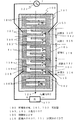
図1は請求項1の発明に係わる共振子型SAWフィルタ(以下略して本素子と称すことがある)の一実施例について、圧電体平板上に形成した電極パターンを図示したものである。
Example 1
FIG. 1 shows an electrode pattern formed on a piezoelectric plate for one embodiment of a resonator-type SAW filter (hereinafter abbreviated as this element) according to the invention of
図1中の各部位の名称は、100は水晶、LiTaO3等からなる圧電体平板、101および102は反射器、103は入力側すだれ状電極、104は出力側すだれ状電極、105は制御用すだれ状電極、106Aおよび106Bは反射器を構成する導体ストリップ、107は給電導体(ブスバー)に接続された入力側すだれ状電極の正極側の電極指、108は給電導体(ブスバー)に接続された入力側すだれ状電極の負極側の電極指、109は給電導体(ブスバー)に接続された出力側すだれ状電極の正極側の電極指、110は給電導体(ブスバー)に接続された出力側すだれ状電極の負極側の電極指である。また、111等は制御用すだれ状電極の電極指、112と113は各々正極側と負極側の入力側給電導体(ブスバー)、114と115は各々正極側と負極側の出力側給電導体(ブスバー)である。さらに、圧電体平板上の123は利用する弾性表面波の位相伝搬方向であるX軸、121は本素子を駆動するための信号源、122は本素子の負荷となるインピーダンスZLである。 In FIG. 1, the names of the respective parts are as follows: 100 is a piezoelectric plate made of quartz, LiTaO 3 , 101 and 102 are reflectors, 103 is an input side interdigital electrode, 104 is an output side interdigital electrode, and 105 is for control Interdigital transducers 106A and 106B are conductor strips constituting the reflector, 107 is an electrode finger on the positive side of the input interdigital transducer connected to the feed conductor (busbar), and 108 is connected to the feed conductor (busbar) An electrode finger on the negative side of the interdigital electrode on the input side, 109 is an electrode finger on the positive side of the interdigital electrode on the output side connected to the power supply conductor (busbar), and 110 is an interdigital shape on the output side connected to the power supply conductor (busbar). It is an electrode finger on the negative electrode side of the electrode. In addition, 111 and the like are electrode fingers of the interdigital electrodes for control, 112 and 113 are input side feeding conductors (busbars) on the positive side and negative side, respectively, and 114 and 115 are output side feeding conductors (busbars) on the positive side and negative side, respectively. ). Further, 123 on the piezoelectric plate is an X-axis that is a phase propagation direction of the surface acoustic wave to be used, 121 is a signal source for driving this element, and 122 is an impedance ZL serving as a load of this element.
さらに説明すると、実線にて区分された116は区間Aに対応する出力側すだれ状電極の部分、117は区間Bに対応する出力側すだれ状電極の部分、実線にて区分された119は区間Aに対応する入力側すだれ状電極の部分、120は区間Bに対応する入力側すだれ状電極部分である。118の区間Cは同一電極周期長PCを有する制御用すだれ状電極の区間である。実際の素子においては、103の入力側すだれ状電極は区間A(119)、区間B(120)・・・のように、区間Aと区間Bを交互に配置して構成されており、また104の出力側すだれ状電極も、区間A(116)、区間B(117)・・・のように、区間Aと区間Bを交互に配置して構成されている。このように構成されたすだれ状電極103と104の前記X軸方向の両側に1対の反射器101と102が配置されている。前記反射器は無くても良い場合があるが、付加すると素子の特性を著しく向上できる。
More specifically, 116 divided by a solid line is a portion of the output interdigital electrode corresponding to the section A, 117 is a portion of the output interdigital electrode corresponding to the section B, and 119 divided by a solid line is the section A. An input side interdigital electrode portion corresponding to, and 120 is an input side interdigital electrode portion corresponding to section B.
さらに説明すると、前記区間Aはすだれ状電極(以下略してIDT:Interdegital Transducerと称す)を構成する正負の電極指を1対として、その対数MAが1対であり、一方、前記区間BはIDTを構成する正負の電極指を1対として、その対数MBが1対かかつ区間Aと区間Bの電極指はいずれも給電導体に接続している。また、前記区間Aは、電極幅寸法Lと電極間寸法Sの和である電極周期長PをP=L+Sとした場合に、電極周期長PがPAであり、前記区間Bは、電極周期長PがPBであるとする。さらに、前記制御用すだれ状電極はそれらの電極周期長PCがPAと異ならしめて形成しかつすだれ状電極の対数MCが全反射係数Γが1程度を成す範囲であるとする。また前記電極周期長については、前記区間Aと区間Bの電極周期長の比PB/PAについて、0.8<PB/PA<1範囲とし、かつ前記制御用すだれ状電極の電極周期長PCと前記PAの比PC/PAを1.01<PC/PA<1.04の範囲に設定する。 More specifically, the section A is a pair of positive and negative electrode fingers constituting an interdigital electrode (hereinafter abbreviated as IDT: Interdegital Transducer), and its logarithm MA is one pair, while the section B is an IDT. The pair of positive and negative electrode fingers is a pair of logarithm MB, and the electrode fingers in the section A and the section B are all connected to the feeding conductor. In the section A, when the electrode period length P that is the sum of the electrode width dimension L and the inter-electrode dimension S is P = L + S, the electrode period length P is PA, and the section B is the electrode period length. Let P be PB. Further, it is assumed that the control interdigital electrodes are formed such that their electrode cycle lengths PC are different from PA, and the logarithm MC of the interdigital electrodes is in a range where the total reflection coefficient Γ is about 1. As for the electrode cycle length, the ratio PB / PA of the electrode cycle lengths of the section A and the section B is in the range of 0.8 <PB / PA <1, and the electrode cycle length PC of the interdigital electrode for control is The PA ratio PC / PA is set in the range of 1.01 <PC / PA <1.04.
図1は全体でいわゆる一般的には縦3重モード型の共振子型SAWフィルタを構成している。 FIG. 1 generally constitutes a so-called generally vertical triple mode resonator type SAW filter.
さらに、前記反射器101、102の中心周波数f(Ref)と、前記区間Bのすだれ状電極が発生する周波数f(IDT)を一致させており、両周波数は区間AのIDTおよび区間BのIDTの電極周期長PAとPBの組み合わせと、反射器101と102の電極周期長PRの関係を適切に設定して、前記f(Ref)=f(IDT)と設定する。 Further, the center frequency f (Ref) of the reflectors 101 and 102 is matched with the frequency f (IDT) generated by the interdigital electrode in the section B. Both frequencies are IDT in the section A and IDT in the section B. The relationship between the combination of the electrode period lengths PA and PB and the electrode period length PR of the reflectors 101 and 102 is appropriately set to set f (Ref) = f (IDT).
以上に述べた図1の構成全体で、入力側のIDTで発生した弾性表面波は1対の反射器101と102で反射して定在波振動状態を形成して利用すべき固有共振モードを発生する。これら固有モードはX軸方向に振動変位が変わる対称モードS0と斜対称モードA0、さらに1次対称モードS1の3個の共振状態であり、前記3個の共振現象を結合して縦3重モード型のSAWフィルタを構成している。ただし、従来の技術と異なる点は、前記区間Aと区間Bの全体が示す反射係数γabが0.01から0.025の範囲であることである。 In the entire configuration of FIG. 1 described above, the surface acoustic wave generated by the IDT on the input side is reflected by a pair of reflectors 101 and 102 to form a standing wave vibration state, and the natural resonance mode to be used is selected. appear. These eigenmodes are the three resonance states of the symmetry mode S0 and the oblique symmetry mode A0 in which the vibration displacement changes in the X-axis direction, and the primary symmetry mode S1. A type SAW filter is formed. However, the difference from the prior art is that the reflection coefficient γab indicated by the entire section A and section B is in the range of 0.01 to 0.025.
さらに構成条件として、前記圧電体平板100と前記IDT(103、104、105等)が有する電極指1本当りの弾性表面波の反射係数γが0.03から0.1の範囲である場合において、本発明の手段は特に有効である。
Further, as a structural condition, when the reflection coefficient γ of the surface acoustic wave per electrode finger included in the piezoelectric
さらにまた、詳細な構成条件をあげると、前記圧電体平板が水晶STWカットであり、前記すだれ状電極はアルミニウム金属により形成されて電極指1本当りの弾性表面波の反射係数γが0.05±0.02であり、かつ前記PB/PAの比が0.91±0.02であり、かつ前記PC/PAの比が1.02であり、かつ前記MAとMBが1対であり、MCが10対から30対範囲の20対であり、区間Aおよび区間Bの電極指を給電導体に接続し、かつ前記入力側すだれ状電極と出力側すだれ状電極の和Mが100±10対であり、特にMC=20対の場合には、入力および出力側のIDTは40対である。かつ前記すだれ状電極の交差指幅WCRが50〜80波長であり、前記反射器の導体本数は30〜100本である場合において特に良好な特性が得られる。この構成条件に対応する前記電極周期長P(X)の詳細設定の一例を図3に示した。図3において、横軸は素子のX座標位置、縦軸は区間Aの電極周期長PAに対するP(X)の比P(X)/PAである。これらの値は、反射器において0.968、入力および出力側IDTの区間Aにおいて1.0、区間Bにおいて0.91、制御IDT区間Cにおいて1.02の値に設定してある。 More specifically, the piezoelectric plate is a quartz STW cut, the interdigital electrode is formed of aluminum metal, and the reflection coefficient γ of the surface acoustic wave per electrode finger is 0.05. ± 0.02, the PB / PA ratio is 0.91 ± 0.02, the PC / PA ratio is 1.02, and the MA and MB are a pair; MC is 20 pairs in the range of 10 to 30 pairs, the electrode fingers of section A and section B are connected to the feeding conductor, and the sum M of the input side interdigital electrode and output side interdigital electrode is 100 ± 10 pairs In particular, when MC = 20 pairs, the IDTs on the input and output sides are 40 pairs. In addition, particularly good characteristics can be obtained when the interdigital finger width WCR of the interdigital electrode is 50 to 80 wavelengths and the number of conductors of the reflector is 30 to 100. An example of the detailed setting of the electrode cycle length P (X) corresponding to this configuration condition is shown in FIG. In FIG. 3, the horizontal axis represents the X coordinate position of the element, and the vertical axis represents the ratio P (X) / PA of P (X) with respect to the electrode period length PA in section A. These values are set to 0.968 in the reflector, 1.0 in the section A of the input and output IDT, 0.91 in the section B, and 1.02 in the control IDT section C.
つぎに、図2において本発明の素子の構造と動作につき説明する。 Next, the structure and operation of the element of the present invention will be described with reference to FIG.
図2は本発明になる図1のような区間Aと区間Bからなる周期的構造を取るIDTを“周波数ポテンシャル設計手法”を活用して表示したものである。図2中の、200と202は前述の区間Aからなるブロックであり、201と203は前述の区間Bからなるブロックである。また、図2中の4つの曲線209等は、弾性表面波の伝搬状態である伝搬帯(斜線領域)および、弾性表面波が伝搬できずに減衰する状態を示めす非伝搬帯(ストップバンドとも呼ばれる白い領域)の特性全体を示す特性曲線であり、波数分散曲線と呼ばれている。波数分散曲線は横軸波数k=2π/λ(1/m)であり、縦軸は周波数FTP(Hz)で表示した。FTPは本発明において活用する“周波数ポテンシャル”の略号である。FTPは利用する弾性表面波の速度をVsとすれば、前述の電極周期長P=PA,PBと、FTP=Vs/(2×P)の関係にある。さらに、基準周波数をFTP0として、周波数の変化率D=(FTP−FTP0)/FTP0で表現することが効率的である。分散曲線上の白丸印204等はIDTによって発生する弾性表面波の動作点を示すもので、208の矢印にて示される右進行波、左進行波が生じている。また206で示される周波数差分量Dは前記の周波数変化率表示であり、区間Aと区間Bの周波数ポテンシャル差である。すなわち、区間AのFTPAは、おおよそFTPA=Vs/(2×PA),区間BのFTPB=Vs/(2×PB)の差D=FTPA−FTPBの関係にある。さらに、205の破線枠で示す領域は、本発明の図1の構成により発生した低反射係数γab(=0〜0.025)をもつ伝搬帯領域である。ちなみに各区間Aおよび区間BはIDTの対数MP(=MA=MB)は検討の結果、1対以上の数対で構成できることがわかった。前記の低反射係数γabをもつ伝搬帯領域の発生メカニズムについては、さらに図5を用いて詳述する。
FIG. 2 shows an IDT having a periodic structure consisting of section A and section B as shown in FIG. 1 according to the present invention, utilizing the “frequency potential design method”. In FIG. 2, 200 and 202 are blocks including the above-described section A, and 201 and 203 are blocks including the above-described section B. In addition, the four
つぎに図4は、0.05の反射係数γを有する基板において、前述の図2の周期的構造を取るIDTを用いて構成した正規型のトランスバーサルフィルタの特性から得られるIDTがもつ全反射係数Γと電極周期長の比PB/PAの関係である。ちなみに前記正規型のトランスバーサルフィルタとは、図1の実施例において反射器101と102が存在しない構成の素子である。図4はまた本発明の前述の実施例1および図2の周期的構造が有する、弾性表面波の反射現象について物理的な特徴を示するものである。図4において、横軸はPB/PAであり、縦軸は前述のΓ値をとって、これらの関係を図示した特性曲線400である。同図4において、PB/PAが0.78±0.02付近(Q点)となると、前記の全反射係数Γがほぼゼロとなっている。また、PB/PA=0.9付近(P点)では、従来品の反射係数に対して約6dBの減少が認められる。これは、基板の反射係数が0.05とすると、約半分の0.25程度となったことが推定できる。
Next, FIG. 4 shows the total reflection of the IDT obtained from the characteristics of the normal type transversal filter constructed using the IDT having the periodic structure shown in FIG. 2 on a substrate having a reflection coefficient γ of 0.05. This is the relationship between the coefficient Γ and the electrode period length ratio PB / PA. Incidentally, the normal type transversal filter is an element having a configuration in which the reflectors 101 and 102 do not exist in the embodiment of FIG. FIG. 4 also shows physical characteristics of the surface acoustic wave reflection phenomenon possessed by the periodic structure of the first embodiment and FIG. 2 of the present invention. In FIG. 4, the horizontal axis is PB / PA, and the vertical axis is the
つぎに図5は、前述のQ点である無反射係数γab=0をもつ伝搬帯領域の発生メカニズムについて図示したものである。図中の縦軸のFは周波数軸であり、右側半面に位置する横軸は、反射係数γの振幅を表し、左側半面に位置した横軸は、前記反射係数γの位相角θであり、反射波の位相角θに相当する。図中の曲線500は前述の区間Aがつくる反射係数γaの振幅特性であり、502は反射係数γaの位相特性である。位相が0度の場合は、反射波は入射波と同位相状態であり、位相が180度の場合には入射波と反射波は逆位相状態であることを意味する。一方、500から上方に周波数変化率にして+0.22シフトした曲線501は、前記区間Bのもつ反射係数γbの振幅特性である。また503はγbの位相特性である。まず区間Aと区間BのIDTはいずれも給電導体に接続しており弾性表面波を励振しかつ500と502の反射特性を有する。500は電極周期長がPAの区間AのIDT対数が4対で、電極指1本当りの反射係数が0.05の場合につき計算したものである(図4に対応)。前記反射特性500においてγ=0となる周波数点は弾性表面波の伝搬点を示すものであり、入射波は反射せずに区間Aを通過する。下側の伝搬点と上側の伝搬点の幅であるストップバンド幅BWは、この場合0.25(25%)の大きな幅となっている。これはIDTの対数MPが4対と極めて小さいことによる。反射特性501は、電極周期長がPBの区間BのIDT対数が4対で、電極指1本当りの反射係数が0.05の場合につき同様に計算したものである。特性501は特性500を0.22(22%)上昇させたもので、これは電極周期長PBがPAの78%に設定されていることによる。特性501のストップバンド幅BWは0.25(25%)であり、区間Aと同一である。前記の励起された弾性表面波は、おおむね振幅動作点B1と位相動作点B2の近傍の周波数成分を持ち、この発生した弾性表面波は、区間Aに至り同一周波数の振幅動作点A1と位相動作点A2で動作する。位相動作点A2とB2は位相がほぼ反転するような配置であり、区間Aと区間Bからの反射波は合成され、相殺されて全体の反射波がゼロとなるため、反射係数γab=0が実現する。従って、前記動作点(B1,B2)のつくる近傍の周波数は無反射の伝搬帯となるわけである。以上が本発明の基礎となる現象の説明である。また、周波数上昇量が0から+0.22の範囲であれば、前記区間Aと区間Bの多数繰り返しが作るトータルな反射係数Γは1から0の間の値を取ることになる。前述の図4の特性はこの状態を示していると解釈できる。
Next, FIG. 5 illustrates the generation mechanism of the propagation band region having the above-described Q point and the non-reflection coefficient γab = 0. The vertical axis F in the figure is the frequency axis, the horizontal axis located on the right half surface represents the amplitude of the reflection coefficient γ, and the horizontal axis located on the left half surface is the phase angle θ of the reflection coefficient γ, This corresponds to the phase angle θ of the reflected wave. A
また区間Bは動作点B1に対応する周波数の弾性表面波を励振して本発明の素子のフィルタ特性を形成する。一方、区間Aの動作点A0に対応する周波数の弾性表面波も励振されるが、こちらは本来のフィルタ特性を阻害するものとなる。そこで本発明においては前述の制御IDTにおいて、電極周期長PCをPAより大きめに設定して、それらが形成する反射特性が前記の動作点A0の弾性表面波を反射するように周波数配置して構成する。図5の502が制御IDTのなす反射特性Γである。
In section B, a surface acoustic wave having a frequency corresponding to the operating point B1 is excited to form the filter characteristics of the element of the present invention. On the other hand, a surface acoustic wave having a frequency corresponding to the operating point A0 in the section A is also excited, but this impedes the original filter characteristics. Therefore, in the present invention, in the control IDT described above, the electrode periodic length PC is set to be larger than PA, and the frequency characteristics are arranged so that the reflection characteristics formed by them reflect the surface acoustic wave at the operating point A0. To do.
本発明は以上の動作原理にもとづき、前記区間Aと区間Bの全体が示す反射係数γabが0.01から0.025の範囲である状態を実現し、対称モードS0と斜対称モードA0、一次対称モードS1の3個の共振状態を利用して、共振子型のSAWフィルタを実現するものである。 Based on the above operation principle, the present invention realizes a state where the reflection coefficient γab indicated by the entire section A and section B is in the range of 0.01 to 0.025, and the symmetrical mode S0 and the obliquely symmetric mode A0, A resonator type SAW filter is realized by utilizing the three resonance states of the symmetric mode S1.
つぎに、本発明の前述の実施例図1が示すフィルタ特性について説明する。 Next, the filter characteristics shown in FIG. 1 will be described.
まず図6は、水晶STWカットが示す反射係数γの特性図である。前記STWカットはオイラー角(φ,θ,ψ)表示で、(0°,127±2°,90°)のものであり、前述の表面集中型のSH波あるいはSSBW弾性表面波と呼ばれる弾性波により動作する。図6の横軸は、電極指の導体幅Lと電極周期長Pとの比である線幅比η=L/Pであり、縦軸は電極指1本当りのもつ反射係数γの値を%表示したものである。図中の特性曲線600は電極膜厚Hに対する弾性表面波の波長λの比が0.03の場合であり、特性曲線601はH/λ=0.05の場合である。仮に素子の動作周波数が1.5GHzの場合については、波長λはSSBW弾性表面波の速度が約5100(m/s)であるから、λ=5100/1.5×10+9=3.4×10-6mであり、この場合のHは、H/λ=0.03において1020×10-10m、H/λ=0.05において1700×10-10mとなる。電極膜の安定な形成においては、1000×10-10m程度の膜厚みが必要であり、この状態における反射係数γは約5〜6%程度となる。
First, FIG. 6 is a characteristic diagram of the reflection coefficient γ indicated by the crystal STW cut. The STW cut is represented by Euler angles (φ, θ, ψ) and is (0 °, 127 ± 2 °, 90 °), and the above-described surface-concentrated SH wave or SSBW surface acoustic wave is called an elastic wave. It works by. The horizontal axis in FIG. 6 is the line width ratio η = L / P, which is the ratio between the conductor width L of the electrode finger and the electrode period length P, and the vertical axis represents the value of the reflection coefficient γ per electrode finger. %. The characteristic curve 600 in the figure is the case where the ratio of the wavelength λ of the surface acoustic wave to the electrode film thickness H is 0.03, and the
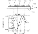
つぎに、図7は前述の反射係数を有する圧電体平板上に本発明の縦3重モード型のSAW共振子を構成した状態を示す概念図である。図中の700は圧電体平板、701と702は反射器、703と704は入力および出力側のIDTであり、これらは区間Aと区間Bを交互に配置して構成してある。705は制御用IDTの領域である。この状態において、前記素子の709のX座標位置に対応して、前記素子において利用する固有の共振モードの振動変位分布U(X)の相対値を図示した。図中の706が対称な変位状態をもつS0モード(基本波)であり、707が斜対称な変位状態をもつA0モード(基本波)である。また、708は1次対称モードS1である。ちなみに、横軸のX座標は1/2波長単位で記述した。
Next, FIG. 7 is a conceptual diagram showing a state in which the longitudinal triple mode type SAW resonator of the present invention is configured on the piezoelectric plate having the reflection coefficient described above. In the figure, 700 is a piezoelectric plate, 701 and 702 are reflectors, and 703 and 704 are input and output side IDTs, which are configured by alternately arranging sections A and B. Reference numeral 705 denotes a control IDT area. In this state, the relative value of the vibration displacement distribution U (X) of the inherent resonance mode used in the element is illustrated corresponding to the X coordinate position of 709 of the element. In the figure, reference numeral 706 denotes an S0 mode (fundamental wave) having a symmetric displacement state, and reference numeral 707 denotes an A0 mode (fundamental wave) having an oblique symmetry displacement state.
ここで、本発明のフィルタの特性を説明する前に、理解を容易ならしめるために、従来技術によって得られるフィルタ特性につき例を示して説明しておく。 Here, before explaining the characteristics of the filter of the present invention, the filter characteristics obtained by the prior art will be described by way of example in order to facilitate understanding.
図8は、本発明において定義した設計変数では、前記H/λ=0.03であり、電極指1本の反射係数が0.05の状態において、従来技術の条件である区間Aと区間Bの電極周期長PAとPBを等しくした場合である。また1区間のIDT対数MP=4対、入力と出力のIDT全体の対数は120対、反射器の本数は80本、電極指の交差幅は50波長の場合である。同図の横軸は、周波数変化率df/f(ppm)であり、縦軸はフィルタの動作伝送量SB(f)デシベル(dB)表示したものである。ちなみに、fは周波数である。特性曲線800が前記のSB(f)特性、800においてピークを示す801がフィルタの通過帯域幅付近を示すものであり、みての通り、単峰性の狭帯域特性を有していることがわかる。本発明はこのような特性状態を改善して、広い通過帯域幅をもたせる手段を提供する。
FIG. 8 shows that the design variable defined in the present invention is H / λ = 0.03, and in the state where the reflection coefficient of one electrode finger is 0.05, section A and section B, which are the conditions of the prior art. This is a case where the electrode cycle lengths PA and PB are equal. Further, the IDT logarithm MP = 4 pairs in one section, the logarithm of the entire input and output IDTs is 120 pairs, the number of reflectors is 80, and the intersection width of the electrode fingers is 50 wavelengths. In the figure, the horizontal axis represents the frequency change rate df / f (ppm), and the vertical axis represents the operation transmission amount SB (f) decibels (dB) of the filter. Incidentally, f is a frequency. The
つぎに、図9は従来の設計条件の場合(PB/PA=1)であり、電極指1本当りの反射係数γの値を変えた場合のフィルタの伝送特性を計算したものである。図9の上段はγ=0.05の場合であり、全IDT対数M=80対、電極指交差幅WCR=100、反射器の導体ストリップ本数N=80、1区間のIDT対数MP=4である。この場合の通過帯の比帯域幅は1200ppmである。また、図9の下段はγ=0.015の場合であり、全IDT対数M=160対と倍に設定し、電極指交差幅WCR=50、N=80、MP=4である。この場合の通過帯の比帯域幅は約1000ppmである。図9が示す意味は、全IDT対数Mを小さくすれば通過帯域幅を広げることができること、反射係数を小さくすれば、全IDT対数Mが大きくても、通過帯域幅を広くすることができることを意味している。本発明は上記の結論であるMを小さくすることと、反射係数を小さくすることを利用して1〜3GHz帯で動作する比帯域幅4000ppmの共振子型SAWフィルタを実現したものである。従来の技術ではすでに述べた通り約500ppmmが限界であった。原因は実用的な電極膜厚みにあっては、反射係数γが5〜10%に至るからである。 Next, FIG. 9 shows the transmission characteristics of the filter when the value of the reflection coefficient γ per electrode finger is changed under the conventional design conditions (PB / PA = 1). The upper part of FIG. 9 shows a case where γ = 0.05, the total IDT logarithm number M = 80 pairs, the electrode finger crossing width WCR = 100, the number of reflector conductor strips N = 80, and the IDT logarithm MP = 4 in one section. is there. In this case, the passband has a specific bandwidth of 1200 ppm. The lower part of FIG. 9 shows a case where γ = 0.015, which is set to double the total IDT logarithm number M = 160 pairs, and electrode finger crossing widths WCR = 50, N = 80, and MP = 4. In this case, the specific bandwidth of the passband is about 1000 ppm. The meaning shown in FIG. 9 is that if the total IDT logarithm M is reduced, the passband width can be widened, and if the reflection coefficient is reduced, the passbandwidth can be widened even if the total IDT logarithm M is large. I mean. The present invention realizes a resonator-type SAW filter having a specific bandwidth of 4000 ppm that operates in the 1 to 3 GHz band by reducing the above-mentioned conclusion M and reducing the reflection coefficient. In the prior art, as already mentioned, about 500 ppmm was the limit. This is because the reflection coefficient γ reaches 5 to 10% in the practical electrode film thickness.
つぎに本発明の図1の実施例が示すフィルタ特性について説明する。 Next, the filter characteristics shown in the embodiment of FIG. 1 of the present invention will be described.
図10はフィルタの伝送特性1001を上段に示し、下段には本素子を構成する反射器の反射特性1002を図示したものである。本発明においては、反射器の中心周波数f(Ref)とフィルタの通過帯域幅の中心周波数f(IDT)を一致させている。このような状態では、区間BのIDTが放射する弾性表面波を完全に反射できるため(反射係数がΓ=1)、反射器の構成本数を少なくできる。このために、反射器の電極周期長PRを0.968PAとした。他の条件は、PPT=PB/PA=0.91であり、全IDT対数M=100対、N=100本、WCR=60波長、MA=MB=1対、制御IDTは20対、Pc/PA=1.02、電極指1本の反射係数は0.05である。前記γが0.05であれば、20本の導体ストリップがあれば、全反射係数Γは1となる勘定であるが、現実には20〜80本、さらには100本程度あれば十分な反射特性が得られる。
FIG. 10 shows the transmission characteristic 1001 of the filter in the upper part, and the lower part shows the reflection characteristic 1002 of the reflector constituting this element. In the present invention, the center frequency f (Ref) of the reflector is matched with the center frequency f (IDT) of the passband width of the filter. In such a state, the surface acoustic wave radiated by the IDT in the section B can be completely reflected (the reflection coefficient is Γ = 1), so that the number of reflectors can be reduced. For this reason, the electrode periodic length PR of the reflector is set to 0.968 PA. Other conditions are PPT = PB / PA = 0.91, total IDT logarithm M = 100 pairs, N = 100, WCR = 60 wavelengths, MA = MB = 1 pair,
つぎに図11は、本発明になる前述の図10の縦3重モード型SAWフィルタを2段縦続接続した場合のフィルタの動作伝送量特性SB(f)をデシベル表示で示したものである。横軸は周波数変化率df/f(ppm)であり、縦軸はフィルタの動作伝送量SB(f)である。本素子はフィルタのインピーダンスが50Ωとなるように設計されている。本素子の動作周波数は1.5GHzとしてある。この場合において伝送特性は上段の図(11−a)の特性曲線1100のようになり、挿入損失の最小値は約2.0dBであり、通過帯域である平坦領域の幅(比帯域幅)は約4000ppmが得られている。また、1101はフィルタの影像インピーダンスZ00(f)(Ω)である。特性曲線1100の周波数9000ppm付近がS1モードであり、1200ppm付近がA0モードであり、14000ppm付近がS0モードである。下段の図(11−b)は周波数範囲を広げた場合のフィルタ特性1102である。帯域外の抑圧特性は一部に狭い周波数を除き50dB程確保されており、良好な特性が得られていることがわかる。また、1103は反射器のもつ反射特性を100倍にしてあわせ表示した。
Next, FIG. 11 shows the operation transmission amount characteristic SB (f) of the filter when the above-described vertical triple mode type SAW filter of FIG. 10 according to the present invention is connected in two stages in decibel display. The horizontal axis represents the frequency change rate df / f (ppm), and the vertical axis represents the filter operation transmission amount SB (f). This element is designed so that the impedance of the filter is 50Ω. The operating frequency of this element is 1.5 GHz. In this case, the transmission characteristic is as shown in the characteristic curve 1100 in the upper diagram (11-a), the minimum value of the insertion loss is about 2.0 dB, and the width of the flat region (specific bandwidth) which is the passband is About 4000 ppm is obtained. Reference numeral 1101 denotes an image impedance Z00 (f) (Ω) of the filter. In the characteristic curve 1100, the vicinity of the frequency of 9000 ppm is the S1 mode, the vicinity of 1200 ppm is the A0 mode, and the vicinity of 14000 ppm is the S0 mode. The lower diagram (11-b) shows the filter characteristics 1102 when the frequency range is expanded. The out-of-band suppression characteristic is secured about 50 dB except for a narrow frequency, and it can be seen that a good characteristic is obtained. Further, 1103 displays the reflection characteristics of the
以上が第1の課題に対する第1の考案の説明である。第1の考案によって発生する側帯波成分の発生(第2の課題)に対するを改善結果をつぎに説明する。この側帯波の発生原因につき解析した結果、発生原因には2つの要因があることがわかった。発生原因の第1は、入力IDTの区間Aと区間Bにおいて弾性表面波の励振の有無にもとずく振幅変調による場合。第2は区間Aと区間Bの電極周期長PA,PBが異なることにより周波数変調によるものである。この観点に立って、図12の状況を説明する。 The above is the description of the first device for the first problem. Next, the improvement result for the generation of the sideband component (second problem) generated by the first device will be described. As a result of analyzing the cause of this sideband wave, it was found that there are two factors in the cause. The first cause of occurrence is due to amplitude modulation based on the presence or absence of surface acoustic wave excitation in the sections A and B of the input IDT. The second is due to frequency modulation due to the difference in the electrode period lengths PA and PB between the section A and the section B. From this viewpoint, the situation of FIG. 12 will be described.
図12は、区間Aの電極指を給電電極に接続しない場合で、かつ区間Aと区間Bの電極指本数NPMを変化させた場合の側帯波の発生状況である。最上段の図(a)はNPM=2本の場合であり、中段の図(b)はNPM=6本の場合いであり、下段の図(c)はNPM=8本の場合である。図中の1200は所望の通過帯域であり、1201、1202、1203の各ピークは、各NPMに対応する側波帯の成分である。これらの振幅の大きさは62dBから30dBと大きく問題である。また、NPMの値は遇数値のものを示したが、奇数値でも同様な側波帯の成分の値を示した。図12において、NPM=2本すなわち、MA=MB=1対の場合が最も側波帯の成分が小さく62dBとなっている。 FIG. 12 shows a sideband generation state when the electrode fingers in the section A are not connected to the feeding electrodes and the number of electrode fingers NPM in the sections A and B is changed. The uppermost figure (a) shows the case of NPM = 2, the middle figure (b) shows the case of NPM = 6, and the lower figure (c) shows the case of NPM = 8. In the figure, 1200 is a desired pass band, and each peak of 1201, 1202 and 1203 is a sideband component corresponding to each NPM. The magnitude of these amplitudes is a large problem from 62 dB to 30 dB. Further, although the value of NPM is a numerical value, even the odd value indicates the value of the same sideband component. In FIG. 12, when NPM = 2 lines, that is, when MA = MB = 1 pair, the sideband component is the smallest and is 62 dB.
そこでつぎに、前述の側波帯成分の発生原因の内の第1の原因を取り除いてみた。すなわち、区間Aの電極指を給電導体に接続してみた。その結果、最小の側波帯成分が実現するNPM=2において、図13のフィルタ特性が得られた。図中の1301は所望の通過帯であり、1302が側波帯の成分である。その大きさは90dBとなって通常のノイズレベルであり使用可能な大きさに改善されているのがわかる。 Then, the first cause of the generation of the sideband components described above was removed. That is, the electrode fingers in the section A were connected to the power supply conductor. As a result, the filter characteristic of FIG. 13 was obtained at NPM = 2 where the minimum sideband component was realized. 1301 in the figure is a desired passband, and 1302 is a sideband component. It can be seen that the magnitude is 90 dB, which is a normal noise level and has been improved to a usable size.
以上のとおり、本発明が水晶のみからなる基板について、STW型の弾性表面波を利用した弾性表面波フィルタの構成および特性につき説明したが、前記基板が水晶以外の材料例えばダイヤモンド基板からなるものでも、また基板表面にSiO2、ZnO、等の薄膜が本素子の特性を損なわない程度に形成されても、本発明の構成条件が満足される範囲であれば有効であることをつけくわえる。 As described above, the configuration and characteristics of the surface acoustic wave filter using STW type surface acoustic waves have been described for the substrate made of only quartz according to the present invention. However, even if the substrate is made of a material other than quartz, for example, a diamond substrate. In addition, even if a thin film such as SiO 2 or ZnO is formed on the substrate surface to such an extent that the characteristics of the element are not impaired, it can be said that it is effective as long as the constitutional conditions of the present invention are satisfied.
最後に、本発明の共振子型SAWフィルタの具体的な用途を考えてみる。 Finally, a specific application of the resonator type SAW filter of the present invention will be considered.
水晶STW基板等を利用して、1.57GHzのRF−フィルタを製作した場合につき特徴を列記すると、
1)周波数温度特性が零温度係数をもち安定である(約-45°〜+85°範囲において、周波数変動量が270ppmと小さい)。
2)材料のQ値が優れ、1.5GHzにおいて共振子のQ値が6000程度と高いため、2dB程度の低損失フィルタが実現できる。
3)区間Aおよび区間Bを周期的に構成しIDTの有する反射係数を低減させて、約3000ppm程度が実現でき、この帯域幅は3MHzの通過帯域幅となって、必要十分にGPS装置に利用される信号の周波数成分範囲2MHzをカバーできる。
4)通過帯域幅内の振幅リップルが小さい50Ωフィルタができる。
The following is a list of features when a 1.57 GHz RF-filter is manufactured using a quartz STW substrate.
1) The frequency temperature characteristic has a zero temperature coefficient and is stable (in the range of about -45 ° to + 85 °, the amount of frequency fluctuation is as small as 270 ppm).
2) Since the Q value of the material is excellent and the Q value of the resonator is as high as about 6000 at 1.5 GHz, a low loss filter of about 2 dB can be realized.
3) Periodic section A and section B are formed periodically to reduce the reflection coefficient of the IDT, and about 3000 ppm can be realized. This bandwidth is a 3 MHz passband and is used for GPS devices as necessary and sufficient. The frequency component range of 2 MHz can be covered.
4) A 50Ω filter with small amplitude ripple within the passband width can be created.
本発明になる前記共振子型のSAWフィルタをGPS装置用のRFフィルタに用いれば、1.57GHzにおいて約3MHzの通過帯域幅が確保でき、従来のLiTaO3基板を用いて作られる通過帯域幅が30MHz程のフィルタに対して、約1/10に装置が受信する雑音レベルが低減できる他、温度環境の変化に対して周波数変動が小さいために、位相変動が少なく低ジッタかつ低位相ノイズなデジタル信号が受信できるため、測地精度にバラツキが無く、高精度な位置精度が計測可能なGPS装置を市場に提供できる。 If the resonator-type SAW filter according to the present invention is used as an RF filter for a GPS device, a pass bandwidth of about 3 MHz can be secured at 1.57 GHz, and a pass bandwidth produced using a conventional LiTaO 3 substrate can be obtained. In addition to reducing the noise level received by the device to about 1/10 of a filter of about 30 MHz, the frequency fluctuation is small with respect to changes in the temperature environment, so there is little phase fluctuation and low jitter and low phase noise digital Since a signal can be received, there is no variation in geodetic accuracy, and a GPS device capable of measuring high-precision position accuracy can be provided to the market.
さらに昨今は、3〜10GHz帯にて使用するUWB(Ultru Wide Band)等の微弱近距離無線が商品化段階にある他、GPS装置とUWBあるいは他の通信装置の近接使用などの手段も研究中であり、本発明の共振子型SAWフィルタはこれらの分野において使用されれば、測地精度の維持のために益々有益な素子となることが考えられる。 Furthermore, recently, in addition to the weak near-field radio such as UWB (Ultra Wide Band) used in the 3-10 GHz band, commercialization stage is also underway, and measures such as the close use of GPS devices and UWB or other communication devices are also being studied. Therefore, if the resonator type SAW filter of the present invention is used in these fields, it is considered that the resonator-type SAW filter becomes an increasingly more useful element for maintaining geodetic accuracy.
100 圧電体平板
101,102 反射器
103,104 入出力IDT
105 制御用IDT
112,113 給電導体
116 区間AのIDT
117 区間BのIDT
100 Piezoelectric plate 101, 102 Reflector 103, 104 Input / output IDT
105 IDT for control
112, 113
117 IDT of section B
Claims (7)
前記の入力側すだれ状電極および出力側すだれ状電極は、前記弾性表面波の波長をλとして電極幅Lがほぼλ/4で構成され、
かつ前記の入力側すだれ状電極および出力側すだれ状電極は、2種類の異なる区間Aと区間Bとを交互に配置してなり、
前記区間Aは、電極幅寸法Lと電極間寸法Sの和である電極周期長PをP=L+Sとした場合に、電極周期長PがPAかつすだれ状電極の対数MAが1対であり、
前記区間Bは、前記電極周期長PがPBかつすだれ状電極の対数MBが1対であり、かつ区間Aと区間Bの電極指はいずれも給電導体に接続し、
さらに、前記制御用すだれ状電極はそれらの電極周期長PCがPAと異ならしめて形成しかつすだれ状電極の対数MCが全反射係数が1程度を成す範囲であることを特徴とする共振子型SAWフィルタ。 An input interdigital electrode for exciting a surface acoustic wave in the phase propagation direction X on the piezoelectric plate, an output interdigital electrode for receiving the surface acoustic wave excited by the input interdigital electrode, and the input interdigital transducer A control interdigital electrode for controlling the state of the surface acoustic wave is provided between the interdigital electrode and the output interdigital transducer, and a pair of reflections are provided on both sides of the input interdigital transducer and the output interdigital transducer. In a resonator type SAW filter having a filter,
The input side interdigital electrode and the output side interdigital electrode are configured such that the wavelength of the surface acoustic wave is λ and the electrode width L is approximately λ / 4.
The input side interdigital electrode and the output side interdigital electrode are formed by alternately arranging two different sections A and B,
In the section A, when the electrode period length P, which is the sum of the electrode width dimension L and the interelectrode dimension S, is P = L + S, the electrode period length P is PA and the logarithm MA of the interdigital electrode is one pair.
In the section B, the electrode cycle length P is PB and the pair of interdigital electrodes MB is one pair, and the electrode fingers of the sections A and B are both connected to the feeding conductors,
Further, the control interdigital electrodes are formed such that their electrode periodic lengths PC are different from PA, and the logarithm MC of the interdigital electrodes is in a range where the total reflection coefficient is about 1. Resonator-type SAW filter.
Priority Applications (1)
| Application Number | Priority Date | Filing Date | Title |
|---|---|---|---|
| JP2004191366A JP2006014165A (en) | 2004-06-29 | 2004-06-29 | Resonator type SAW filter |
Applications Claiming Priority (1)
| Application Number | Priority Date | Filing Date | Title |
|---|---|---|---|
| JP2004191366A JP2006014165A (en) | 2004-06-29 | 2004-06-29 | Resonator type SAW filter |
Publications (1)
| Publication Number | Publication Date |
|---|---|
| JP2006014165A true JP2006014165A (en) | 2006-01-12 |
Family
ID=35780813
Family Applications (1)
| Application Number | Title | Priority Date | Filing Date |
|---|---|---|---|
| JP2004191366A Withdrawn JP2006014165A (en) | 2004-06-29 | 2004-06-29 | Resonator type SAW filter |
Country Status (1)
| Country | Link |
|---|---|
| JP (1) | JP2006014165A (en) |
Cited By (3)
| Publication number | Priority date | Publication date | Assignee | Title |
|---|---|---|---|---|
| JP2009027671A (en) * | 2007-07-24 | 2009-02-05 | Seiko Epson Corp | SH type bulk wave resonator |
| CN114337583A (en) * | 2021-12-03 | 2022-04-12 | 中国科学院上海微系统与信息技术研究所 | A surface acoustic wave resonator |
| CN116318036A (en) * | 2023-05-15 | 2023-06-23 | 成都频岢微电子有限公司 | Surface acoustic wave resonators, surface acoustic wave filters and duplexers |
-
2004
- 2004-06-29 JP JP2004191366A patent/JP2006014165A/en not_active Withdrawn
Cited By (5)
| Publication number | Priority date | Publication date | Assignee | Title |
|---|---|---|---|---|
| JP2009027671A (en) * | 2007-07-24 | 2009-02-05 | Seiko Epson Corp | SH type bulk wave resonator |
| CN114337583A (en) * | 2021-12-03 | 2022-04-12 | 中国科学院上海微系统与信息技术研究所 | A surface acoustic wave resonator |
| CN114337583B (en) * | 2021-12-03 | 2024-03-29 | 中国科学院上海微系统与信息技术研究所 | Surface acoustic wave resonator |
| CN116318036A (en) * | 2023-05-15 | 2023-06-23 | 成都频岢微电子有限公司 | Surface acoustic wave resonators, surface acoustic wave filters and duplexers |
| CN116318036B (en) * | 2023-05-15 | 2023-09-22 | 成都频岢微电子有限公司 | Surface acoustic wave resonators, surface acoustic wave filters and duplexers |
Similar Documents
| Publication | Publication Date | Title |
|---|---|---|
| KR100346805B1 (en) | Surface acoustic wave device | |
| KR100609966B1 (en) | Surface acoustic wave filter apparatus and communication apparatus | |
| JP3391309B2 (en) | Surface wave device and communication device | |
| JP4100249B2 (en) | Surface acoustic wave device, communication device | |
| JP2015109574A (en) | Longitudinal coupling resonator type surface acoustic wave filter and communication instrument | |
| JP2005065160A (en) | Surface acoustic wave device and manufacturing method thereof | |
| JPH08288788A (en) | Surface acoustic wave element | |
| KR102561687B1 (en) | Transducer structure for source suppression in SAW filter devices | |
| JP2013168864A (en) | Elastic surface wave element and electronic component | |
| JP4432968B2 (en) | Resonator type SAW filter | |
| WO2000067374A1 (en) | Transverse double mode saw filter | |
| JP2011041127A (en) | Elastic wave device | |
| JP2002204142A (en) | Reflective end face type surface wave device | |
| JP2006014165A (en) | Resonator type SAW filter | |
| JP4145678B2 (en) | Vertical double mode SAW filter | |
| JP4582150B2 (en) | Surface acoustic wave device and module device or oscillation circuit using the same | |
| JP2005303893A (en) | Resonator type SAW filter | |
| JP2005204042A (en) | Surface acoustic wave resonator and surface acoustic wave filter | |
| JP2004260402A (en) | Surface acoustic wave device and communication device having it | |
| JPWO2007004661A1 (en) | Surface acoustic wave device | |
| JP3597483B2 (en) | Surface acoustic wave device | |
| JP2003298383A (en) | Surface acoustic wave device | |
| JP4310928B2 (en) | Surface acoustic wave device | |
| JP2006165746A (en) | Surface acoustic wave device | |
| JPH1093384A (en) | 2-port SAW resonator |
Legal Events
| Date | Code | Title | Description |
|---|---|---|---|
| A300 | Withdrawal of application because of no request for examination |
Free format text: JAPANESE INTERMEDIATE CODE: A300 Effective date: 20070904 |