JP2006019431A - 半導体装置およびそれを用いた半導体モジュール - Google Patents
半導体装置およびそれを用いた半導体モジュール Download PDFInfo
- Publication number
- JP2006019431A JP2006019431A JP2004194673A JP2004194673A JP2006019431A JP 2006019431 A JP2006019431 A JP 2006019431A JP 2004194673 A JP2004194673 A JP 2004194673A JP 2004194673 A JP2004194673 A JP 2004194673A JP 2006019431 A JP2006019431 A JP 2006019431A
- Authority
- JP
- Japan
- Prior art keywords
- electrode
- semiconductor device
- cylindrical
- insulating film
- conductor
- Prior art date
- Legal status (The legal status is an assumption and is not a legal conclusion. Google has not performed a legal analysis and makes no representation as to the accuracy of the status listed.)
- Granted
Links
Images




Classifications
-
- H—ELECTRICITY
- H10—SEMICONDUCTOR DEVICES; ELECTRIC SOLID-STATE DEVICES NOT OTHERWISE PROVIDED FOR
- H10W—GENERIC PACKAGES, INTERCONNECTIONS, CONNECTORS OR OTHER CONSTRUCTIONAL DETAILS OF DEVICES COVERED BY CLASS H10
- H10W90/00—Package configurations
-
- H—ELECTRICITY
- H10—SEMICONDUCTOR DEVICES; ELECTRIC SOLID-STATE DEVICES NOT OTHERWISE PROVIDED FOR
- H10W—GENERIC PACKAGES, INTERCONNECTIONS, CONNECTORS OR OTHER CONSTRUCTIONAL DETAILS OF DEVICES COVERED BY CLASS H10
- H10W20/00—Interconnections in chips, wafers or substrates
- H10W20/01—Manufacture or treatment
- H10W20/021—Manufacture or treatment of interconnections within wafers or substrates
- H10W20/023—Manufacture or treatment of interconnections within wafers or substrates the interconnections being through-semiconductor vias
- H10W20/0245—Manufacture or treatment of interconnections within wafers or substrates the interconnections being through-semiconductor vias comprising use of blind vias during the manufacture
-
- H—ELECTRICITY
- H10—SEMICONDUCTOR DEVICES; ELECTRIC SOLID-STATE DEVICES NOT OTHERWISE PROVIDED FOR
- H10W—GENERIC PACKAGES, INTERCONNECTIONS, CONNECTORS OR OTHER CONSTRUCTIONAL DETAILS OF DEVICES COVERED BY CLASS H10
- H10W20/00—Interconnections in chips, wafers or substrates
- H10W20/20—Interconnections within wafers or substrates, e.g. through-silicon vias [TSV]
-
- H—ELECTRICITY
- H10—SEMICONDUCTOR DEVICES; ELECTRIC SOLID-STATE DEVICES NOT OTHERWISE PROVIDED FOR
- H10W—GENERIC PACKAGES, INTERCONNECTIONS, CONNECTORS OR OTHER CONSTRUCTIONAL DETAILS OF DEVICES COVERED BY CLASS H10
- H10W20/00—Interconnections in chips, wafers or substrates
- H10W20/20—Interconnections within wafers or substrates, e.g. through-silicon vias [TSV]
- H10W20/211—Through-semiconductor vias, e.g. TSVs
- H10W20/212—Top-view shapes or dispositions, e.g. top-view layouts of the vias
- H10W20/2125—Top-view shapes
-
- H—ELECTRICITY
- H10—SEMICONDUCTOR DEVICES; ELECTRIC SOLID-STATE DEVICES NOT OTHERWISE PROVIDED FOR
- H10W—GENERIC PACKAGES, INTERCONNECTIONS, CONNECTORS OR OTHER CONSTRUCTIONAL DETAILS OF DEVICES COVERED BY CLASS H10
- H10W20/00—Interconnections in chips, wafers or substrates
- H10W20/20—Interconnections within wafers or substrates, e.g. through-silicon vias [TSV]
- H10W20/211—Through-semiconductor vias, e.g. TSVs
- H10W20/217—Through-semiconductor vias, e.g. TSVs comprising ring-shaped isolation structures outside of the via holes
-
- H—ELECTRICITY
- H10—SEMICONDUCTOR DEVICES; ELECTRIC SOLID-STATE DEVICES NOT OTHERWISE PROVIDED FOR
- H10W—GENERIC PACKAGES, INTERCONNECTIONS, CONNECTORS OR OTHER CONSTRUCTIONAL DETAILS OF DEVICES COVERED BY CLASS H10
- H10W42/00—Arrangements for protection of devices
-
- H—ELECTRICITY
- H10—SEMICONDUCTOR DEVICES; ELECTRIC SOLID-STATE DEVICES NOT OTHERWISE PROVIDED FOR
- H10W—GENERIC PACKAGES, INTERCONNECTIONS, CONNECTORS OR OTHER CONSTRUCTIONAL DETAILS OF DEVICES COVERED BY CLASS H10
- H10W72/00—Interconnections or connectors in packages
- H10W72/071—Connecting or disconnecting
- H10W72/072—Connecting or disconnecting of bump connectors
- H10W72/07251—Connecting or disconnecting of bump connectors characterised by changes in properties of the bump connectors during connecting
-
- H—ELECTRICITY
- H10—SEMICONDUCTOR DEVICES; ELECTRIC SOLID-STATE DEVICES NOT OTHERWISE PROVIDED FOR
- H10W—GENERIC PACKAGES, INTERCONNECTIONS, CONNECTORS OR OTHER CONSTRUCTIONAL DETAILS OF DEVICES COVERED BY CLASS H10
- H10W72/00—Interconnections or connectors in packages
- H10W72/20—Bump connectors, e.g. solder bumps or copper pillars; Dummy bumps; Thermal bumps
-
- H—ELECTRICITY
- H10—SEMICONDUCTOR DEVICES; ELECTRIC SOLID-STATE DEVICES NOT OTHERWISE PROVIDED FOR
- H10W—GENERIC PACKAGES, INTERCONNECTIONS, CONNECTORS OR OTHER CONSTRUCTIONAL DETAILS OF DEVICES COVERED BY CLASS H10
- H10W72/00—Interconnections or connectors in packages
- H10W72/20—Bump connectors, e.g. solder bumps or copper pillars; Dummy bumps; Thermal bumps
- H10W72/241—Dispositions, e.g. layouts
- H10W72/244—Dispositions, e.g. layouts relative to underlying supporting features, e.g. bond pads, RDLs or vias
-
- H—ELECTRICITY
- H10—SEMICONDUCTOR DEVICES; ELECTRIC SOLID-STATE DEVICES NOT OTHERWISE PROVIDED FOR
- H10W—GENERIC PACKAGES, INTERCONNECTIONS, CONNECTORS OR OTHER CONSTRUCTIONAL DETAILS OF DEVICES COVERED BY CLASS H10
- H10W72/00—Interconnections or connectors in packages
- H10W72/20—Bump connectors, e.g. solder bumps or copper pillars; Dummy bumps; Thermal bumps
- H10W72/241—Dispositions, e.g. layouts
- H10W72/247—Dispositions of multiple bumps
- H10W72/248—Top-view layouts, e.g. mirror arrays
-
- H—ELECTRICITY
- H10—SEMICONDUCTOR DEVICES; ELECTRIC SOLID-STATE DEVICES NOT OTHERWISE PROVIDED FOR
- H10W—GENERIC PACKAGES, INTERCONNECTIONS, CONNECTORS OR OTHER CONSTRUCTIONAL DETAILS OF DEVICES COVERED BY CLASS H10
- H10W72/00—Interconnections or connectors in packages
- H10W72/20—Bump connectors, e.g. solder bumps or copper pillars; Dummy bumps; Thermal bumps
- H10W72/29—Bond pads specially adapted therefor
-
- H—ELECTRICITY
- H10—SEMICONDUCTOR DEVICES; ELECTRIC SOLID-STATE DEVICES NOT OTHERWISE PROVIDED FOR
- H10W—GENERIC PACKAGES, INTERCONNECTIONS, CONNECTORS OR OTHER CONSTRUCTIONAL DETAILS OF DEVICES COVERED BY CLASS H10
- H10W72/00—Interconnections or connectors in packages
- H10W72/90—Bond pads, in general
- H10W72/921—Structures or relative sizes of bond pads
- H10W72/922—Bond pads being integral with underlying chip-level interconnections
- H10W72/9226—Bond pads being integral with underlying chip-level interconnections with via interconnections
-
- H—ELECTRICITY
- H10—SEMICONDUCTOR DEVICES; ELECTRIC SOLID-STATE DEVICES NOT OTHERWISE PROVIDED FOR
- H10W—GENERIC PACKAGES, INTERCONNECTIONS, CONNECTORS OR OTHER CONSTRUCTIONAL DETAILS OF DEVICES COVERED BY CLASS H10
- H10W72/00—Interconnections or connectors in packages
- H10W72/90—Bond pads, in general
- H10W72/921—Structures or relative sizes of bond pads
- H10W72/923—Bond pads having multiple stacked layers
-
- H—ELECTRICITY
- H10—SEMICONDUCTOR DEVICES; ELECTRIC SOLID-STATE DEVICES NOT OTHERWISE PROVIDED FOR
- H10W—GENERIC PACKAGES, INTERCONNECTIONS, CONNECTORS OR OTHER CONSTRUCTIONAL DETAILS OF DEVICES COVERED BY CLASS H10
- H10W72/00—Interconnections or connectors in packages
- H10W72/90—Bond pads, in general
- H10W72/931—Shapes of bond pads
-
- H—ELECTRICITY
- H10—SEMICONDUCTOR DEVICES; ELECTRIC SOLID-STATE DEVICES NOT OTHERWISE PROVIDED FOR
- H10W—GENERIC PACKAGES, INTERCONNECTIONS, CONNECTORS OR OTHER CONSTRUCTIONAL DETAILS OF DEVICES COVERED BY CLASS H10
- H10W72/00—Interconnections or connectors in packages
- H10W72/90—Bond pads, in general
- H10W72/931—Shapes of bond pads
- H10W72/932—Plan-view shape, i.e. in top view
-
- H—ELECTRICITY
- H10—SEMICONDUCTOR DEVICES; ELECTRIC SOLID-STATE DEVICES NOT OTHERWISE PROVIDED FOR
- H10W—GENERIC PACKAGES, INTERCONNECTIONS, CONNECTORS OR OTHER CONSTRUCTIONAL DETAILS OF DEVICES COVERED BY CLASS H10
- H10W90/00—Package configurations
- H10W90/701—Package configurations characterised by the relative positions of pads or connectors relative to package parts
- H10W90/721—Package configurations characterised by the relative positions of pads or connectors relative to package parts of bump connectors
- H10W90/722—Package configurations characterised by the relative positions of pads or connectors relative to package parts of bump connectors between stacked chips
-
- H—ELECTRICITY
- H10—SEMICONDUCTOR DEVICES; ELECTRIC SOLID-STATE DEVICES NOT OTHERWISE PROVIDED FOR
- H10W—GENERIC PACKAGES, INTERCONNECTIONS, CONNECTORS OR OTHER CONSTRUCTIONAL DETAILS OF DEVICES COVERED BY CLASS H10
- H10W90/00—Package configurations
- H10W90/701—Package configurations characterised by the relative positions of pads or connectors relative to package parts
- H10W90/721—Package configurations characterised by the relative positions of pads or connectors relative to package parts of bump connectors
- H10W90/724—Package configurations characterised by the relative positions of pads or connectors relative to package parts of bump connectors between a chip and a stacked insulating package substrate, interposer or RDL
Landscapes
- Internal Circuitry In Semiconductor Integrated Circuit Devices (AREA)
Abstract
【解決手段】 半導体装置100は、シリコン基板101と、シリコン基板101を貫通する断面矩形の貫通孔中に充填された構造体120を設ける。構造体120は、筒状貫通電極103と、ストライプ状貫通電極107と、シリコン105と、第一の絶縁膜109と、第二の絶縁膜111と、第三の絶縁膜113と、を備える。筒状貫通電極103を、シリコン基板101を貫通する筒状の導電体とする。また、ストライプ状貫通電極107を、シリコン基板101を貫通し、筒状貫通電極103の内側に筒状貫通電極103から離間して設ける。筒状貫通電極103の内側の領域に、複数の貫通電極107を互いに略平行に設ける。
【選択図】 図1
Description
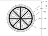
本実施形態は、貫通電極を備えた半導体装置に関する。半導体基板に一または二以上のストライプ状の貫通電極が近接配置され、そのストライプ状の貫通電極の外側を、所定の幅の筒状貫通電極が囲んでいる。
図3は、本実施形態に係る半導体装置の構成を模式的に示す断面図である。また、図4は、図3のB−B’断面図である。図3および図4に示したように、半導体装置110は、シリコン基板101およびシリコン基板101中を貫通する構造体130を備える。構造体130は、貫通電極131、シリコン119、第一の絶縁膜109および第二の絶縁膜133を備える。
以上の実施形態に記載の半導体装置は、マルチチップモジュール等に好適に用いることができる。マルチチップモジュールは、たとえば以上の実施形態に係る半導体装置と他の半導体装置とが積層されており、シリコン基板101を貫通する貫通電極と他の半導体装置の導電部材とが電気的に接続された構成とすることができる。
101 シリコン基板
103 筒状貫通電極
105 シリコン
105 絶縁膜
107 ストライプ状貫通電極
109 第一の絶縁膜
110 半導体装置
111 第二の絶縁膜
113 第三の絶縁膜
115 筒状貫通電極
117 ストライプ状貫通電極
119 シリコン
120 構造体
121 開口部
123 開口部
125 絶縁膜
127 導電膜
129 絶縁膜
130 構造体
131 貫通電極
133 第二の絶縁膜
135 バンプ
137 プリント配線基板
Claims (5)
- 半導体基板と、
前記半導体基板を貫通する筒状の第一導電体と、
前記半導体基板を貫通し、前記第一導電体の内側に前記第一導電体から離間して設けられた複数の第二導電体と、
を備えることを特徴とする半導体装置。 - 請求項1に記載の半導体装置において、複数の前記第二導電体は、互いに略平行に設けられていることを特徴とする半導体装置。
- 半導体基板と、
前記半導体基板を貫通する筒状の第一導電体と、
前記半導体基板を貫通し、前記第一導電体の内面の一の領域と他の領域とを接続する第二導電体と、
を備えることを特徴とする半導体装置。 - 請求項3に記載の半導体装置において、互いに略平行に設けられた複数の前記第二導電体を含むことを特徴とする半導体装置。
- 請求項1乃至4いずれかに記載の半導体装置と、他の半導体装置とが積層されてなる半導体モジュールであって、
前記第一導電体または前記第二導電体と、前記他の半導体装置とが、電気的に接続されていることを特徴とする半導体モジュール。
Priority Applications (3)
| Application Number | Priority Date | Filing Date | Title |
|---|---|---|---|
| JP2004194673A JP4568039B2 (ja) | 2004-06-30 | 2004-06-30 | 半導体装置およびそれを用いた半導体モジュール |
| US11/167,162 US7768133B2 (en) | 2004-06-30 | 2005-06-28 | Semiconductor device and semiconductor module employing thereof |
| US12/820,478 US7898073B2 (en) | 2004-06-30 | 2010-06-22 | Semiconductor device and semiconductor module employing thereof |
Applications Claiming Priority (1)
| Application Number | Priority Date | Filing Date | Title |
|---|---|---|---|
| JP2004194673A JP4568039B2 (ja) | 2004-06-30 | 2004-06-30 | 半導体装置およびそれを用いた半導体モジュール |
Publications (2)
| Publication Number | Publication Date |
|---|---|
| JP2006019431A true JP2006019431A (ja) | 2006-01-19 |
| JP4568039B2 JP4568039B2 (ja) | 2010-10-27 |
Family
ID=35540454
Family Applications (1)
| Application Number | Title | Priority Date | Filing Date |
|---|---|---|---|
| JP2004194673A Expired - Fee Related JP4568039B2 (ja) | 2004-06-30 | 2004-06-30 | 半導体装置およびそれを用いた半導体モジュール |
Country Status (2)
| Country | Link |
|---|---|
| US (2) | US7768133B2 (ja) |
| JP (1) | JP4568039B2 (ja) |
Cited By (10)
| Publication number | Priority date | Publication date | Assignee | Title |
|---|---|---|---|---|
| JP2006261403A (ja) * | 2005-03-17 | 2006-09-28 | Elpida Memory Inc | 半導体装置 |
| JP2007165461A (ja) * | 2005-12-12 | 2007-06-28 | Elpida Memory Inc | 半導体装置及びその製造方法 |
| JP2008244187A (ja) * | 2007-03-28 | 2008-10-09 | Elpida Memory Inc | 貫通電極および半導体装置 |
| JP2010219425A (ja) * | 2009-03-18 | 2010-09-30 | Toshiba Corp | 半導体装置 |
| US7897459B2 (en) | 2006-09-28 | 2011-03-01 | Elpida Memory, Inc. | Semiconductor device and manufacturing method thereof |
| US8685854B2 (en) | 2010-03-12 | 2014-04-01 | Renesas Electronics Corporation | Method of forming a via in a semiconductor device |
| US8836138B2 (en) | 2011-09-09 | 2014-09-16 | Shinko Electric Industries Co., Ltd. | Wiring substrate and semiconductor package |
| WO2023112689A1 (ja) * | 2021-12-13 | 2023-06-22 | ソニーセミコンダクタソリューションズ株式会社 | 半導体装置およびその製造方法、並びに電子機器 |
| US11690297B2 (en) | 2019-11-22 | 2023-06-27 | Seiko Epson Corporation | Vibration device |
| US11818958B2 (en) | 2019-09-30 | 2023-11-14 | Seiko Epson Corporation | Vibration device |
Families Citing this family (39)
| Publication number | Priority date | Publication date | Assignee | Title |
|---|---|---|---|---|
| JP4795677B2 (ja) * | 2004-12-02 | 2011-10-19 | ルネサスエレクトロニクス株式会社 | 半導体装置およびそれを用いた半導体モジュール、ならびに半導体装置の製造方法 |
| US7633167B2 (en) * | 2005-09-29 | 2009-12-15 | Nec Electronics Corporation | Semiconductor device and method for manufacturing same |
| KR100826979B1 (ko) * | 2006-09-30 | 2008-05-02 | 주식회사 하이닉스반도체 | 스택 패키지 및 그 제조방법 |
| US9085727B2 (en) | 2006-12-08 | 2015-07-21 | Schlumberger Technology Corporation | Heterogeneous proppant placement in a fracture with removable extrametrical material fill |
| US7581590B2 (en) * | 2006-12-08 | 2009-09-01 | Schlumberger Technology Corporation | Heterogeneous proppant placement in a fracture with removable channelant fill |
| US8636065B2 (en) | 2006-12-08 | 2014-01-28 | Schlumberger Technology Corporation | Heterogeneous proppant placement in a fracture with removable channelant fill |
| US8757259B2 (en) * | 2006-12-08 | 2014-06-24 | Schlumberger Technology Corporation | Heterogeneous proppant placement in a fracture with removable channelant fill |
| US8763699B2 (en) | 2006-12-08 | 2014-07-01 | Schlumberger Technology Corporation | Heterogeneous proppant placement in a fracture with removable channelant fill |
| FR2910368B1 (fr) | 2006-12-22 | 2012-03-09 | Rhodia Operations | Perles de polyamides et procede de fabrication de ces perles |
| US8936082B2 (en) | 2007-07-25 | 2015-01-20 | Schlumberger Technology Corporation | High solids content slurry systems and methods |
| US8490698B2 (en) | 2007-07-25 | 2013-07-23 | Schlumberger Technology Corporation | High solids content methods and slurries |
| US9040468B2 (en) | 2007-07-25 | 2015-05-26 | Schlumberger Technology Corporation | Hydrolyzable particle compositions, treatment fluids and methods |
| US8490699B2 (en) | 2007-07-25 | 2013-07-23 | Schlumberger Technology Corporation | High solids content slurry methods |
| US10011763B2 (en) | 2007-07-25 | 2018-07-03 | Schlumberger Technology Corporation | Methods to deliver fluids on a well site with variable solids concentration from solid slurries |
| US9080440B2 (en) | 2007-07-25 | 2015-07-14 | Schlumberger Technology Corporation | Proppant pillar placement in a fracture with high solid content fluid |
| US8384224B2 (en) | 2008-08-08 | 2013-02-26 | International Business Machines Corporation | Through wafer vias and method of making same |
| US8299566B2 (en) * | 2008-08-08 | 2012-10-30 | International Business Machines Corporation | Through wafer vias and method of making same |
| US8138036B2 (en) | 2008-08-08 | 2012-03-20 | International Business Machines Corporation | Through silicon via and method of fabricating same |
| US8035198B2 (en) * | 2008-08-08 | 2011-10-11 | International Business Machines Corporation | Through wafer via and method of making same |
| JP2010074106A (ja) * | 2008-09-22 | 2010-04-02 | Nec Electronics Corp | 半導体チップ、半導体ウェーハおよびそのダイシング方法 |
| US8662172B2 (en) | 2010-04-12 | 2014-03-04 | Schlumberger Technology Corporation | Methods to gravel pack a well using expanding materials |
| US8505628B2 (en) | 2010-06-30 | 2013-08-13 | Schlumberger Technology Corporation | High solids content slurries, systems and methods |
| US8511381B2 (en) | 2010-06-30 | 2013-08-20 | Schlumberger Technology Corporation | High solids content slurry methods and systems |
| US8607870B2 (en) | 2010-11-19 | 2013-12-17 | Schlumberger Technology Corporation | Methods to create high conductivity fractures that connect hydraulic fracture networks in a well |
| US8742477B1 (en) * | 2010-12-06 | 2014-06-03 | Xilinx, Inc. | Elliptical through silicon vias for active interposers |
| US9133387B2 (en) | 2011-06-06 | 2015-09-15 | Schlumberger Technology Corporation | Methods to improve stability of high solid content fluid |
| JP5998459B2 (ja) * | 2011-11-15 | 2016-09-28 | ローム株式会社 | 半導体装置およびその製造方法、電子部品 |
| US9803457B2 (en) | 2012-03-08 | 2017-10-31 | Schlumberger Technology Corporation | System and method for delivering treatment fluid |
| US9863228B2 (en) | 2012-03-08 | 2018-01-09 | Schlumberger Technology Corporation | System and method for delivering treatment fluid |
| TWI478326B (zh) * | 2012-08-09 | 2015-03-21 | Macronix Int Co Ltd | 半導體多層結構及其製造方法 |
| US8816423B2 (en) * | 2012-08-13 | 2014-08-26 | Macronix International Co., Ltd. | Semiconducting multi-layer structure and method for manufacturing the same |
| US10622310B2 (en) | 2012-09-26 | 2020-04-14 | Ping-Jung Yang | Method for fabricating glass substrate package |
| US9615453B2 (en) * | 2012-09-26 | 2017-04-04 | Ping-Jung Yang | Method for fabricating glass substrate package |
| US9528354B2 (en) | 2012-11-14 | 2016-12-27 | Schlumberger Technology Corporation | Downhole tool positioning system and method |
| US9388335B2 (en) | 2013-07-25 | 2016-07-12 | Schlumberger Technology Corporation | Pickering emulsion treatment fluid |
| US10229877B2 (en) | 2016-06-22 | 2019-03-12 | Nanya Technology Corporation | Semiconductor chip and multi-chip package using thereof |
| US10002844B1 (en) | 2016-12-21 | 2018-06-19 | Invensas Bonding Technologies, Inc. | Bonded structures |
| US10508030B2 (en) | 2017-03-21 | 2019-12-17 | Invensas Bonding Technologies, Inc. | Seal for microelectronic assembly |
| US12374641B2 (en) | 2019-06-12 | 2025-07-29 | Adeia Semiconductor Bonding Technologies Inc. | Sealed bonded structures and methods for forming the same |
Citations (4)
| Publication number | Priority date | Publication date | Assignee | Title |
|---|---|---|---|---|
| JPH10223833A (ja) * | 1996-12-02 | 1998-08-21 | Toshiba Corp | マルチチップ半導体装置、ならびにマルチチップ半導体装置用チップおよびその形成方法 |
| JP2002043502A (ja) * | 2000-07-25 | 2002-02-08 | Toshiba Corp | マルチチップ半導体装置、ならびにマルチチップ半導体装置用チップ及びその製造方法 |
| JP2003151978A (ja) * | 2001-10-18 | 2003-05-23 | Hewlett Packard Co <Hp> | ウェーハの諸部分を電気的に分離するためのシステム |
| JP2005285972A (ja) * | 2004-03-29 | 2005-10-13 | Sharp Corp | 伝送線路形成方法、伝送線路、半導体チップおよび半導体集積回路ユニット |
Family Cites Families (5)
| Publication number | Priority date | Publication date | Assignee | Title |
|---|---|---|---|---|
| US6052287A (en) * | 1997-12-09 | 2000-04-18 | Sandia Corporation | Silicon ball grid array chip carrier |
| US6531945B1 (en) * | 2000-03-10 | 2003-03-11 | Micron Technology, Inc. | Integrated circuit inductor with a magnetic core |
| JP4522574B2 (ja) | 2000-12-04 | 2010-08-11 | 大日本印刷株式会社 | 半導体装置の作製方法 |
| US6579738B2 (en) * | 2000-12-15 | 2003-06-17 | Micron Technology, Inc. | Method of alignment for buried structures formed by surface transformation of empty spaces in solid state materials |
| JP2002289623A (ja) | 2001-03-28 | 2002-10-04 | Toshiba Corp | 半導体装置及びその製造方法 |
-
2004
- 2004-06-30 JP JP2004194673A patent/JP4568039B2/ja not_active Expired - Fee Related
-
2005
- 2005-06-28 US US11/167,162 patent/US7768133B2/en not_active Expired - Lifetime
-
2010
- 2010-06-22 US US12/820,478 patent/US7898073B2/en not_active Expired - Fee Related
Patent Citations (4)
| Publication number | Priority date | Publication date | Assignee | Title |
|---|---|---|---|---|
| JPH10223833A (ja) * | 1996-12-02 | 1998-08-21 | Toshiba Corp | マルチチップ半導体装置、ならびにマルチチップ半導体装置用チップおよびその形成方法 |
| JP2002043502A (ja) * | 2000-07-25 | 2002-02-08 | Toshiba Corp | マルチチップ半導体装置、ならびにマルチチップ半導体装置用チップ及びその製造方法 |
| JP2003151978A (ja) * | 2001-10-18 | 2003-05-23 | Hewlett Packard Co <Hp> | ウェーハの諸部分を電気的に分離するためのシステム |
| JP2005285972A (ja) * | 2004-03-29 | 2005-10-13 | Sharp Corp | 伝送線路形成方法、伝送線路、半導体チップおよび半導体集積回路ユニット |
Cited By (11)
| Publication number | Priority date | Publication date | Assignee | Title |
|---|---|---|---|---|
| JP2006261403A (ja) * | 2005-03-17 | 2006-09-28 | Elpida Memory Inc | 半導体装置 |
| JP2007165461A (ja) * | 2005-12-12 | 2007-06-28 | Elpida Memory Inc | 半導体装置及びその製造方法 |
| US7897459B2 (en) | 2006-09-28 | 2011-03-01 | Elpida Memory, Inc. | Semiconductor device and manufacturing method thereof |
| JP2008244187A (ja) * | 2007-03-28 | 2008-10-09 | Elpida Memory Inc | 貫通電極および半導体装置 |
| JP2010219425A (ja) * | 2009-03-18 | 2010-09-30 | Toshiba Corp | 半導体装置 |
| CN102361032A (zh) * | 2009-03-18 | 2012-02-22 | 株式会社东芝 | 半导体装置 |
| US8685854B2 (en) | 2010-03-12 | 2014-04-01 | Renesas Electronics Corporation | Method of forming a via in a semiconductor device |
| US8836138B2 (en) | 2011-09-09 | 2014-09-16 | Shinko Electric Industries Co., Ltd. | Wiring substrate and semiconductor package |
| US11818958B2 (en) | 2019-09-30 | 2023-11-14 | Seiko Epson Corporation | Vibration device |
| US11690297B2 (en) | 2019-11-22 | 2023-06-27 | Seiko Epson Corporation | Vibration device |
| WO2023112689A1 (ja) * | 2021-12-13 | 2023-06-22 | ソニーセミコンダクタソリューションズ株式会社 | 半導体装置およびその製造方法、並びに電子機器 |
Also Published As
| Publication number | Publication date |
|---|---|
| US7898073B2 (en) | 2011-03-01 |
| US7768133B2 (en) | 2010-08-03 |
| JP4568039B2 (ja) | 2010-10-27 |
| US20100258918A1 (en) | 2010-10-14 |
| US20060006539A1 (en) | 2006-01-12 |
Similar Documents
| Publication | Publication Date | Title |
|---|---|---|
| JP4568039B2 (ja) | 半導体装置およびそれを用いた半導体モジュール | |
| US7964972B2 (en) | Semiconductor device providing a first electrical conductor and a second electrical conductor in one through hole and method for manufacturing the same | |
| US7842610B2 (en) | Semiconductor device | |
| JP4795677B2 (ja) | 半導体装置およびそれを用いた半導体モジュール、ならびに半導体装置の製造方法 | |
| JP5412506B2 (ja) | 半導体装置 | |
| CN114520219A (zh) | 半导体封装 | |
| KR100804596B1 (ko) | 반도체장치 | |
| US20110298097A1 (en) | Semiconductor device and method for manufacturing the same | |
| KR102833169B1 (ko) | 반도체 장치 및 반도체 장치의 제조 방법 | |
| TWI691033B (zh) | 新穎的貫穿矽觸點結構及其形成方法 | |
| JP2015079960A (ja) | 集積回路素子及びその製造方法 | |
| US20240379623A1 (en) | Semiconductor package structure and method for forming the same | |
| CN102760710B (zh) | 硅穿孔结构及其形成方法 | |
| JP3685722B2 (ja) | 半導体装置及びその製造方法 | |
| US11469174B2 (en) | Semiconductor device | |
| US10256201B2 (en) | Bonding pad structure having island portions and method for manufacturing the same | |
| US20240071923A1 (en) | Semiconductor device | |
| US12543545B2 (en) | Redistribution layer and methods of fabrication thereof | |
| US20260052668A1 (en) | Semiconductor device and method of manufacturing the same | |
| CN120784171A (zh) | 半导体管芯封装和形成其的方法 | |
| CN120341201A (zh) | 硅穿孔结构及其电路 | |
| US7075136B2 (en) | System-on-chip including DRAM and analog device for improving DRAM capacitance and method for fabricating the same |
Legal Events
| Date | Code | Title | Description |
|---|---|---|---|
| A621 | Written request for application examination |
Free format text: JAPANESE INTERMEDIATE CODE: A621 Effective date: 20070208 |
|
| A977 | Report on retrieval |
Free format text: JAPANESE INTERMEDIATE CODE: A971007 Effective date: 20090430 |
|
| A131 | Notification of reasons for refusal |
Free format text: JAPANESE INTERMEDIATE CODE: A131 Effective date: 20090512 |
|
| A521 | Request for written amendment filed |
Free format text: JAPANESE INTERMEDIATE CODE: A523 Effective date: 20090713 |
|
| A131 | Notification of reasons for refusal |
Free format text: JAPANESE INTERMEDIATE CODE: A131 Effective date: 20091208 |
|
| A521 | Request for written amendment filed |
Free format text: JAPANESE INTERMEDIATE CODE: A523 Effective date: 20100208 |
|
| TRDD | Decision of grant or rejection written | ||
| A01 | Written decision to grant a patent or to grant a registration (utility model) |
Free format text: JAPANESE INTERMEDIATE CODE: A01 Effective date: 20100803 |
|
| A01 | Written decision to grant a patent or to grant a registration (utility model) |
Free format text: JAPANESE INTERMEDIATE CODE: A01 |
|
| A61 | First payment of annual fees (during grant procedure) |
Free format text: JAPANESE INTERMEDIATE CODE: A61 Effective date: 20100806 |
|
| R150 | Certificate of patent or registration of utility model |
Ref document number: 4568039 Country of ref document: JP Free format text: JAPANESE INTERMEDIATE CODE: R150 Free format text: JAPANESE INTERMEDIATE CODE: R150 |
|
| FPAY | Renewal fee payment (event date is renewal date of database) |
Free format text: PAYMENT UNTIL: 20130813 Year of fee payment: 3 |
|
| S111 | Request for change of ownership or part of ownership |
Free format text: JAPANESE INTERMEDIATE CODE: R313113 |
|
| R350 | Written notification of registration of transfer |
Free format text: JAPANESE INTERMEDIATE CODE: R350 |
|
| R250 | Receipt of annual fees |
Free format text: JAPANESE INTERMEDIATE CODE: R250 |
|
| R250 | Receipt of annual fees |
Free format text: JAPANESE INTERMEDIATE CODE: R250 |
|
| R250 | Receipt of annual fees |
Free format text: JAPANESE INTERMEDIATE CODE: R250 |
|
| R250 | Receipt of annual fees |
Free format text: JAPANESE INTERMEDIATE CODE: R250 |
|
| R250 | Receipt of annual fees |
Free format text: JAPANESE INTERMEDIATE CODE: R250 |
|
| R250 | Receipt of annual fees |
Free format text: JAPANESE INTERMEDIATE CODE: R250 |
|
| LAPS | Cancellation because of no payment of annual fees |