JP2006032010A - Organic EL display device - Google Patents
Organic EL display device Download PDFInfo
- Publication number
- JP2006032010A JP2006032010A JP2004206105A JP2004206105A JP2006032010A JP 2006032010 A JP2006032010 A JP 2006032010A JP 2004206105 A JP2004206105 A JP 2004206105A JP 2004206105 A JP2004206105 A JP 2004206105A JP 2006032010 A JP2006032010 A JP 2006032010A
- Authority
- JP
- Japan
- Prior art keywords
- organic
- electrode
- layer
- display device
- light emitting
- Prior art date
- Legal status (The legal status is an assumption and is not a legal conclusion. Google has not performed a legal analysis and makes no representation as to the accuracy of the status listed.)
- Pending
Links
Images
Classifications
-
- H—ELECTRICITY
- H10—SEMICONDUCTOR DEVICES; ELECTRIC SOLID-STATE DEVICES NOT OTHERWISE PROVIDED FOR
- H10K—ORGANIC ELECTRIC SOLID-STATE DEVICES
- H10K59/00—Integrated devices, or assemblies of multiple devices, comprising at least one organic light-emitting element covered by group H10K50/00
- H10K59/30—Devices specially adapted for multicolour light emission
- H10K59/38—Devices specially adapted for multicolour light emission comprising colour filters or colour changing media [CCM]
-
- H—ELECTRICITY
- H10—SEMICONDUCTOR DEVICES; ELECTRIC SOLID-STATE DEVICES NOT OTHERWISE PROVIDED FOR
- H10K—ORGANIC ELECTRIC SOLID-STATE DEVICES
- H10K59/00—Integrated devices, or assemblies of multiple devices, comprising at least one organic light-emitting element covered by group H10K50/00
- H10K59/80—Constructional details
- H10K59/87—Passivation; Containers; Encapsulations
- H10K59/871—Self-supporting sealing arrangements
- H10K59/8722—Peripheral sealing arrangements, e.g. adhesives, sealants
-
- H—ELECTRICITY
- H10—SEMICONDUCTOR DEVICES; ELECTRIC SOLID-STATE DEVICES NOT OTHERWISE PROVIDED FOR
- H10K—ORGANIC ELECTRIC SOLID-STATE DEVICES
- H10K50/00—Organic light-emitting devices
- H10K50/80—Constructional details
- H10K50/86—Arrangements for improving contrast, e.g. preventing reflection of ambient light
- H10K50/865—Arrangements for improving contrast, e.g. preventing reflection of ambient light comprising light absorbing layers, e.g. light-blocking layers
-
- H—ELECTRICITY
- H10—SEMICONDUCTOR DEVICES; ELECTRIC SOLID-STATE DEVICES NOT OTHERWISE PROVIDED FOR
- H10K—ORGANIC ELECTRIC SOLID-STATE DEVICES
- H10K59/00—Integrated devices, or assemblies of multiple devices, comprising at least one organic light-emitting element covered by group H10K50/00
- H10K59/10—OLED displays
- H10K59/12—Active-matrix OLED [AMOLED] displays
- H10K59/122—Pixel-defining structures or layers, e.g. banks
-
- H—ELECTRICITY
- H10—SEMICONDUCTOR DEVICES; ELECTRIC SOLID-STATE DEVICES NOT OTHERWISE PROVIDED FOR
- H10K—ORGANIC ELECTRIC SOLID-STATE DEVICES
- H10K59/00—Integrated devices, or assemblies of multiple devices, comprising at least one organic light-emitting element covered by group H10K50/00
- H10K59/80—Constructional details
- H10K59/8791—Arrangements for improving contrast, e.g. preventing reflection of ambient light
- H10K59/8792—Arrangements for improving contrast, e.g. preventing reflection of ambient light comprising light absorbing layers, e.g. black layers
Landscapes
- Electroluminescent Light Sources (AREA)
Abstract
【課題】 高精細なフルカラー表示のためのカラーフィルタや色変換層を低コストで製作する。
【解決手段】 基板SUBの主面上に、画素毎に成膜された第1電極CDと、該各第1電極上を共通に覆って形成された白色発光能を有する有機EL層OLE(W)と、該有機EL層を共通に覆って形成された第2電極ADとをこの順で積層した有機EL発光層を有し、有機EL層OLE(W)の発光々を第2電極AD側に出射するごとく構成し、第2電極ADの上層で、有機EL発光層からの白色光を所定の色に変換する湿式工程で塗布されたカラーフィルタFILを画素毎に有し、当該第2電極ADとカラーフィルタFILとの間に、該カラーフィルタの塗布材料による前記発光層の劣化を防止するための保護層PASを設けた。
【選択図】 図1
PROBLEM TO BE SOLVED: To produce a color filter and a color conversion layer for high-definition full color display at a low cost.
SOLUTION: On a main surface of a substrate SUB, a first electrode CD formed for each pixel and an organic EL layer OLE (W) having a white light emitting ability formed so as to cover each first electrode in common. ) And the second electrode AD formed so as to cover the organic EL layer in common, and the organic EL light emitting layer OLE (W) emits light emitted from the second electrode AD side. Each pixel has a color filter FIL applied in a wet process for converting white light from the organic EL light-emitting layer into a predetermined color above the second electrode AD. A protective layer PAS for preventing deterioration of the light emitting layer due to the color filter coating material was provided between the AD and the color filter FIL.
[Selection] Figure 1
Description
本発明は、表示装置に係り、白色発光の有機EL素子とカラーフィルタとを組み合わせて多色表示を行うようにした有機EL表示装置に好適なものである。 The present invention relates to a display device, and is suitable for an organic EL display device which performs multicolor display by combining a white light emitting organic EL element and a color filter.
近年、高度情報化社会の到来に伴い、パソコン、カーナビ、携帯情報端末、情報通信機器あるいはこれらの複合製品の需要が増大している。これらの製品の表示手段には、薄型、軽量、低消費電力のディスプレイデバイスが適しており、補助照明を用いる液晶表示装置、あるいは有機ELなどの自発光型の電気光学素子を用いた表示装置やプラズマ表示装置も実用化されている。 In recent years, with the advent of an advanced information society, demand for personal computers, car navigation systems, portable information terminals, information communication devices, or composite products of these has increased. Display devices of these products are suitable for thin, light, and low power consumption display devices, such as liquid crystal display devices using auxiliary illumination, or display devices using self-luminous electro-optic elements such as organic EL. Plasma display devices have also been put into practical use.
この種の表示装置では、カラー表示を実現するために、複数色(通常は、赤(R)、緑(G)、青(B)の3色)の単位画素を隣接して配置し、それぞれの単位画素ごとに色層(カラーフィルタ、あるいは発色層)を形成して、所謂フルカラー表示を実現している。 In this type of display device, in order to realize color display, unit pixels of a plurality of colors (usually, three colors of red (R), green (G), and blue (B)) are arranged adjacent to each other, A so-called full color display is realized by forming a color layer (color filter or coloring layer) for each unit pixel.
フルカラー表示の有機ELの製造プロセスでは、有機EL層の形成にマスク蒸着法を用いた3色塗り分けが行われている。スループットの向上や製造コストの低減のために、多面取りの可能な大サイズ基板を用いた場合、マスク蒸着法ではマスクの製作精度、位置合わせ精度に限界があり、また、蒸発源からの熱輻射によるマスクの寸法変化が発生し易いため、高い歩留まりを達成することは難しい。さらに、蒸着雰囲気における異物対策やマスク交換に時間を要するために製造設備の稼動率が下がる。 In the manufacturing process of full-color display organic EL, three-color coating using a mask vapor deposition method is performed for forming an organic EL layer. When using a large-size substrate that can be multi-faced to improve throughput and reduce manufacturing costs, the mask vapor deposition method has limitations in mask manufacturing accuracy and alignment accuracy, and heat radiation from the evaporation source. Therefore, it is difficult to achieve a high yield because the dimensional change of the mask easily occurs. Furthermore, since it takes time for foreign matter countermeasures and mask replacement in the vapor deposition atmosphere, the operating rate of the manufacturing facility is lowered.
この対策のために、以下に説明するような従来技術がある。特許文献1、特許文献2は、有機EL素子を形成した第1の基板と、ホトリソグラフィー(以下、ホトリソ)手法で色変換フィルタを形成した第2の基板を所定の間隙で貼り合わせたトップエミッション構造の有機EL表示装置を開示する。特許文献3は、平滑な透明基板上に濡れ性可変層を設けて、濡れ性の違いを利用して選択的に各カラーフィルタ用染料を被着させる液晶パネル用フィルタの製造方法を開示する。特許文献4は、白色有機EL素子にカラーフィルタを組み合わせてフルカラー表示を実現する有機EL表示装置を開示する。特許文献5は、発光部材と色素変換部材およびカラーフィルタの組み合わせで高効率の3原色発光を可能とする表示素子を開示する。 For this countermeasure, there are conventional techniques as described below. Patent Document 1 and Patent Document 2 describe a top emission in which a first substrate on which an organic EL element is formed and a second substrate on which a color conversion filter is formed by a photolithography (hereinafter referred to as photolithography) technique are bonded together with a predetermined gap. An organic EL display device having a structure is disclosed. Patent Document 3 discloses a method for producing a filter for a liquid crystal panel in which a wettability variable layer is provided on a smooth transparent substrate and each color filter dye is selectively applied using the difference in wettability. Patent Document 4 discloses an organic EL display device that realizes full-color display by combining a color filter with a white organic EL element. Patent Document 5 discloses a display element that can emit light of three primary colors with high efficiency by a combination of a light emitting member, a dye conversion member, and a color filter.
以上の文献の他に、関連する従来技術を開示したものとして、特許文献6、特許文献7、特許文献8、特許文献9、特許文献10、特許文献11、および特許文献12を挙げることができる。
特許文献1および特許文献2に開示の従来技術では、発光部側とカラーフィルタ側の双方の基板の位置合わせにずれが生じ易く、高精細化は困難である。また、カラーフィルタの形成をホトリソ手法で製作するのを基本としているため、コスト高となる。特許文献3に開示された濡れ性可変層を設けるため、材料やプロセスが増加し、コスト高を解決するものでない。特許文献4および特許文献5に開示の従来技術でも同様に、材料やプロセスが増加し、コスト高は解決されない。特許文献6から特許文献10は、比較的低温で薄膜を形成する技術を開示する。特許文献11と特許文献12は、トップエミッション型の有機EL表示装置におけるカラーフィルタや色変換層の形成技術を開示するが、高精細なフルカラー表示のためのカラーフィルタや色変換層を低コストで製作することを開示しない。 In the prior art disclosed in Patent Document 1 and Patent Document 2, misalignment is likely to occur in the alignment of the substrates on both the light emitting unit side and the color filter side, and high definition is difficult. Further, since the color filter is basically manufactured by a photolithography method, the cost is increased. Since the wettability variable layer disclosed in Patent Document 3 is provided, the number of materials and processes increases, and the cost is not solved. Similarly, in the conventional techniques disclosed in Patent Document 4 and Patent Document 5, the number of materials and processes increases, and the high cost is not solved. Patent Documents 6 to 10 disclose techniques for forming a thin film at a relatively low temperature. Patent Document 11 and Patent Document 12 disclose a technology for forming a color filter and a color conversion layer in a top emission type organic EL display device. However, a color filter and a color conversion layer for high-definition full-color display are provided at low cost. Does not disclose production.
本発明の目的は、高精細なフルカラー表示のためのカラーフィルタや色変換層を低コストで製作することを可能とした有機EL表示装置を提供することにある。 An object of the present invention is to provide an organic EL display device capable of manufacturing a color filter and a color conversion layer for high-definition full-color display at a low cost.
上記目的を達成するため、本発明の有機EL表示装置は、基板の主面上に、画素毎に成膜された第1電極と、該各第1電極上を共通に覆って形成された白色発光能を有する有機EL層と、該有機EL層を共通に覆って形成された第2電極とをこの順で積層した有機EL発光層を有し、前記有機EL層の発光々を前記第2電極側に出射するごとく構成し、
前記第2電極の上層で、前記有機EL発光層からの白色光を所定の色に変換する湿式工程で塗布されたカラーフィルタを前記画素毎に有し、当該第2電極と前記カラーフィルタとの間に、該カラーフィルタの塗布材料による前記発光層の劣化を防止するための保護層を設けた。
In order to achieve the above object, an organic EL display device according to the present invention includes a first electrode formed for each pixel on a main surface of a substrate, and a white color formed so as to cover the first electrode in common. An organic EL light emitting layer in which an organic EL layer having light emitting ability and a second electrode formed so as to cover the organic EL layer in common are stacked in this order, and the light emitted from the organic EL layer is emitted from the second electrode. Configure as if it is emitted to the electrode side,
Each pixel has a color filter applied in a wet process for converting white light from the organic EL light emitting layer into a predetermined color above the second electrode, and between the second electrode and the color filter. A protective layer for preventing the light emitting layer from being deteriorated by the color filter coating material was provided therebetween.
上記目的を達成するため、本発明は、基板の主面(例えば、有機EL表示装置の表示画面に対応)上に、複数の第1電極(その各々は表示画面の画素に対応)と、該各第1電極上を共通に覆って形成された白色発光能を有する有機EL層と、複数の第1電極を共通に覆って(例えば、表示画面全体に亘って)拡がり且つ白色発光能を有する有機EL層と、(有機EL層の発光機能を補助する他の有機材料層を含めてもよい)と、有機EL層上で前記複数の第1電極を共通に覆う(例えば、表示画面全体に拡がる)第2電極とをこの順で積層して、前記基板主面内に前記複数の第1電極の一つ、前記有機EL層、及び前記第2電極を夫々含む複数の有機EL発光素子が配置(例えば、二次元的に)され、且つ前記有機EL層からの発光を前記第2電極側に出射する有機EL表示装置を提供する。 In order to achieve the above object, the present invention provides a plurality of first electrodes (each corresponding to a pixel of a display screen) on a main surface of a substrate (for example, corresponding to a display screen of an organic EL display device), An organic EL layer having a white light emitting ability formed so as to cover each first electrode in common and a plurality of first electrodes commonly covered (for example, over the entire display screen) and have a white light emitting ability. An organic EL layer (which may include other organic material layers that assist the light emitting function of the organic EL layer), and the plurality of first electrodes are commonly covered on the organic EL layer (for example, over the entire display screen) A plurality of organic EL light-emitting elements each including one of the plurality of first electrodes, the organic EL layer, and the second electrode in the main surface of the substrate. Disposed (for example, two-dimensionally) and emits light from the organic EL layer. An organic EL display device which emits the electrode side.
本発明の第1の観点に拠れば、斯様に構成される有機EL表示装置の前記第2電極の上部(above the Second Electrode)には、前記有機EL層から発せられた白色光を所定の色に変換するカラーフィルタが湿式工程で塗布される。カラーフィルタは、前記有機EL発光素子毎(換言すれば、画素毎)に分けるとよく、複数のカラーフィルタの各々を有機EL層及び第2電極を介して複数の第1電極の一つと対向するように配置するとよい。この第2電極とカラーフィルタとの間には、カラーフィルタの塗布材料(例えば、前記湿式工程で用いられる材料)による前記有機EL層の劣化を防止する保護層が設けられる。 According to the first aspect of the present invention, white light emitted from the organic EL layer is given to the upper part (above the Second Electrode) of the organic EL display device thus configured. A color filter that converts to a color is applied in a wet process. The color filter may be divided for each organic EL light emitting element (in other words, for each pixel), and each of the plurality of color filters is opposed to one of the plurality of first electrodes through the organic EL layer and the second electrode. It is good to arrange like this. A protective layer is provided between the second electrode and the color filter to prevent deterioration of the organic EL layer due to a color filter coating material (for example, a material used in the wet process).
また、本発明の第2の観点に拠れば、上述の如く構成される有機EL表示装置の前記第2電極の上には、この第2電極の表面を平坦にする平坦化層が設けられ、この平坦化層上又は上部(on or above the Leveling Layer)には、前記有機EL層から発せられた白色光を所定の色に変換するカラーフィルタが湿式工程での塗布により前記有機EL発光素子毎(換言すれば、画素毎)に形成される。前記カラーフィルタは、基板主面内に配置された前記複数の有機EL発光素子の夫々に対応した複数個の各々を、これに対応する有機EL発光素子の上部(有機EL発光素子を介して基板主面とは反対側)に配置するとよい。複数のカラーフィルタの各々は、有機EL層、第2電極、及び平坦化層を介して複数の第1電極の一つと対向するように配置するとよい。 According to the second aspect of the present invention, a flattening layer for flattening the surface of the second electrode is provided on the second electrode of the organic EL display device configured as described above. A color filter that converts white light emitted from the organic EL layer into a predetermined color is applied to each of the organic EL light emitting elements by applying it in a wet process on or above the leveling layer. (In other words, each pixel). The color filter includes a plurality of organic EL light emitting elements arranged in the main surface of the substrate, each corresponding to an upper portion of the corresponding organic EL light emitting element (the substrate via the organic EL light emitting element). It may be arranged on the opposite side of the main surface. Each of the plurality of color filters may be disposed so as to face one of the plurality of first electrodes through the organic EL layer, the second electrode, and the planarization layer.
さらに、本発明の第3の観点に拠れば、上述の如く構成される有機EL表示装置の前記第2電極の上部(above the Second Electrode)には、前記有機EL層から発せられた光の波長を所定の波長に変換する波長変換フィルタが前記有機EL発光素子毎(換言すれば、画素毎)に湿式工程における塗布で形成され、前記波長変換フィルタの各々の上部(above each of the Wavelength Converting Filters)には、当該波長変換フィルタを通した光を所定の色に変換するカラーフィルタが前記有機EL発光素子毎(換言すれば、画素毎)に湿式工程における塗布で形成される。前記第2電極と前記波長変換フィルタとの間には、この波長変換フィルタの塗布材料(例えば、前記波長変換フィルタを形成するための湿式工程で用いられる材料)による前記有機EL層の劣化を防止するための第1の保護層が設けられ、前記波長変換フィルタと前記カラーフィルタとの間には、このカラーフィルタの塗布材料(例えば、前記カラーフィルタを形成するための湿式工程で用いられる材料)による前記有機EL層の劣化を防止するための第2の保護層が設けられる。 Furthermore, according to the third aspect of the present invention, the wavelength of light emitted from the organic EL layer is formed above the second electrode of the organic EL display device configured as described above. A wavelength conversion filter for converting the wavelength conversion filter into a predetermined wavelength is formed by application in a wet process for each organic EL light emitting element (in other words, for each pixel), and above each of the wavelength conversion filters (above each of the wavelength converting filters) ), A color filter that converts light passing through the wavelength conversion filter into a predetermined color is formed by application in a wet process for each organic EL light emitting element (in other words, for each pixel). Between the second electrode and the wavelength conversion filter, deterioration of the organic EL layer due to a coating material of the wavelength conversion filter (for example, a material used in a wet process for forming the wavelength conversion filter) is prevented. A first protective layer is provided, and a coating material for the color filter (for example, a material used in a wet process for forming the color filter) is provided between the wavelength conversion filter and the color filter. A second protective layer for preventing deterioration of the organic EL layer due to is provided.
波長変換フィルタは、色変換層とも呼ばれ、これに入射する光の波長プロファイル(波長に対する強度分布)を、この材料における電子エネルギー準位間の励起と失活とにより変える。従って、カラーフィルタがこれに入射する光を所定の波長帯域にて選択的に出射させるのに対し、波長変換フィルタはこれに入射する光をその波長プロファイルを異ならせて(例えば、最大強度を示す波長をシフトさせて)出射させる。 The wavelength conversion filter is also called a color conversion layer, and changes the wavelength profile (intensity distribution with respect to wavelength) of light incident thereon by excitation and deactivation between electron energy levels in this material. Therefore, the color filter selectively emits light incident on the color filter in a predetermined wavelength band, whereas the wavelength conversion filter varies the wavelength profile of the light incident on the color filter (for example, exhibits a maximum intensity). The light is emitted with a shifted wavelength.
本発明の第3の観点に拠る有機EL表示装置では、前記波長変換フィルタを、前記基板主面内に配置された前記複数の有機EL発光素子の夫々に対応させて複数個に分け、その各々をこれに対応する有機EL発光素子の上部(有機EL発光素子を介して基板主面とは反対側)に配置するとよい。複数の波長変換フィルタの各々は、前記有機EL層、前記第2電極、及び前記第1の保護層を介して前記複数の第1電極の一つと対向するように配置されるとよい。一方、前記カラーフィルタは、当該複数の波長変換フィルタの夫々に対応させて複数個に分け、その各々を前記第2の保護層を介して複数の波長変換フィルタの対応する一つと対向させて配置するとよい。。 In the organic EL display device according to the third aspect of the present invention, the wavelength conversion filter is divided into a plurality corresponding to each of the plurality of organic EL light emitting elements arranged in the main surface of the substrate, and each of them. May be arranged on the upper part of the organic EL light emitting element corresponding to this (on the side opposite to the main surface of the substrate through the organic EL light emitting element). Each of the plurality of wavelength conversion filters may be disposed to face one of the plurality of first electrodes through the organic EL layer, the second electrode, and the first protective layer. On the other hand, the color filter is divided into a plurality corresponding to each of the plurality of wavelength conversion filters, and each of the color filters is arranged to face a corresponding one of the plurality of wavelength conversion filters via the second protective layer. Good. .
なお、本発明は上記の構成および後述する実施例の構成に限定されるものではなく、本発明の技術思想を逸脱することなく、種々の変形が可能であることは言うまでもない。 Note that the present invention is not limited to the above-described configuration and the configuration of the embodiments described later, and it goes without saying that various modifications can be made without departing from the technical idea of the present invention.
本発明によれば、高精細なフルカラー表示のためのカラーフィルタや色変換層(波長変換フィルタ)を高位置精度、低コストで塗布することが可能となり、高品質の画像表示を 可能とした有機EL表示装置を提供することができる。 According to the present invention, it is possible to apply a color filter and a color conversion layer (wavelength conversion filter) for high-definition full-color display with high positional accuracy and low cost, and an organic material that enables high-quality image display. An EL display device can be provided.
以下、本発明の実施の形態について、実施例の図面を参照して詳細に説明する。 Embodiments of the present invention will be described below in detail with reference to the drawings of the embodiments.
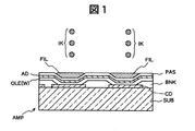
図1は、本発明の実施例1を説明する断面図である。図1に示した基板AMPは有機EL表示装置を構成するアクティブ・マトリクス基板(または、薄膜トランジスタ基板、TFT基板と略称)である。TFT基板AMPは、絶縁性の基板(ここではガラス基板)SUBの主面に第1電極である陰極CDが画素ごとに形成されている。陰極CDは、導電性金属膜のパターニングで形成される。導電性金属膜としては、アルミニウム(Al)とフッ化リチウム(LiF)を用いた。なお、この他にMg/Al, Mg/Inなどでもよい。これらの導電性金属膜を蒸着あるいはスパッタリング、もしくはCVDなどでガラス基板SUBの主面に成膜し、ホトリソ工程などを用いて所要のパターニングを施し、画素毎の陰極CDを形成する。陰極CDは反射性が良好であることが望ましい。 FIG. 1 is a cross-sectional view illustrating Example 1 of the present invention. A substrate AMP shown in FIG. 1 is an active matrix substrate (or abbreviated as a thin film transistor substrate or a TFT substrate) constituting an organic EL display device. In the TFT substrate AMP, a cathode CD as a first electrode is formed for each pixel on the main surface of an insulating substrate (here, a glass substrate) SUB. The cathode CD is formed by patterning a conductive metal film. As the conductive metal film, aluminum (Al) and lithium fluoride (LiF) were used. In addition, Mg / Al, Mg / In, etc. may be used. These conductive metal films are deposited on the main surface of the glass substrate SUB by vapor deposition, sputtering, CVD, or the like, and subjected to necessary patterning using a photolithography process or the like, thereby forming a cathode CD for each pixel. It is desirable that the cathode CD has good reflectivity.
次に、陰極CDを覆う絶縁膜(以下、層間膜)が形成される。この層間膜は、窒化珪素(SiN)等の無機材料を、陰極CDも含めた基板SUB主面に化学気相成長法(Chemical Vapor Deposition)で形成してもよく、または、ノボラック系樹脂(Novolak resin)等の有機材料を当該基板SUB主面に塗布し、これを硬化させて形成してもよい。この層間膜を、陰極CDの上面を露呈する如くパターニングして隔壁提(以下、バンクとも称する)BNKを形成する。バンクBNKで囲まれる陰極CDの上面を含む領域が一つの画素(カラー表示の副画素)に対応する。 Next, an insulating film (hereinafter referred to as an interlayer film) covering the cathode CD is formed. This interlayer film may be formed of an inorganic material such as silicon nitride (SiN) on the main surface of the substrate SUB including the cathode CD by chemical vapor deposition, or a novolak resin (Novolak resin). An organic material such as resin) may be applied to the main surface of the substrate SUB and cured. This interlayer film is patterned so as to expose the upper surface of the cathode CD to form a partition wall (hereinafter also referred to as a bank) BNK. A region including the upper surface of the cathode CD surrounded by the bank BNK corresponds to one pixel (color display sub-pixel).
バンクBNKおよび陰極CDの上方を覆って有機発光層OLEを形成する。典型的には、有機発光層OLEはマスク蒸着法で形成するが、有機発光層OLEの材料次第では、インクジェット法、薄膜形成後のホトリソ工程によるパターニングなどの方法を用いることもできる。実施例1ではマスク蒸着法を採用して、電子輸送層(Alq)、第1有機発光層、第2有機発光層、ホール輸送層(α―NPD)を順に積層した。第1有機発光層には、ホストが出光興産製BH―120で、ドーパントとして同社製RD−001Xを用いた。また、第2有機発光層には、ホストが出光興産製BH―120で、ドーパントとして同社製BD−102を用いた。これら第1有機発光層と第2有機発光層の両者で白色発光の有機発光層OLE(W)が得られる。 An organic light emitting layer OLE is formed so as to cover the bank BNK and the cathode CD. Typically, the organic light emitting layer OLE is formed by a mask vapor deposition method, but depending on the material of the organic light emitting layer OLE, a method such as an ink jet method or patterning by a photolithography process after forming a thin film can be used. In Example 1, a mask vapor deposition method was employed, and an electron transport layer (Alq), a first organic light emitting layer, a second organic light emitting layer, and a hole transport layer (α-NPD) were sequentially laminated. For the first organic light emitting layer, the host was BH-120 manufactured by Idemitsu Kosan, and RD-001X manufactured by the same company was used as a dopant. In the second organic light emitting layer, the host was BH-120 manufactured by Idemitsu Kosan, and BD-102 manufactured by the same company was used as the dopant. Both the first organic light emitting layer and the second organic light emitting layer provide a white light emitting organic light emitting layer OLE (W).
この有機発光層OLE(W)の前面を覆ってITOを成膜し、第2電極である透明陽極ADを形成する。透明陽極ADはITOに限らず、透明金属膜などの他の透明導電膜であれば良い。そして、透明陽極ADの上面に保護層PASを形成する。有機発光層OLE(W)、透明陽極AD、保護層PASはバンクBNKの形状に倣った表面形状(凹部)を有する。保護層PASは有機発光層OLE(W)の保護、次工程のインクジェット法によるカラーフィルタ形成での濡れ性を制御する目的で形成する。保護層PASはまた、インクジェットで塗布されるカラーフィルタ材料(インク)による有機発光層OLE(W)の特性劣化を防止する。 An ITO film is formed so as to cover the front surface of the organic light emitting layer OLE (W), and a transparent anode AD as a second electrode is formed. The transparent anode AD is not limited to ITO, and may be another transparent conductive film such as a transparent metal film. Then, the protective layer PAS is formed on the upper surface of the transparent anode AD. The organic light emitting layer OLE (W), the transparent anode AD, and the protective layer PAS have a surface shape (concave portion) that follows the shape of the bank BNK. The protective layer PAS is formed for the purpose of protecting the organic light emitting layer OLE (W) and controlling the wettability in the color filter formation by the inkjet method in the next step. The protective layer PAS also prevents deterioration of the characteristics of the organic light emitting layer OLE (W) due to the color filter material (ink) applied by inkjet.
保護層PASの材料は、窒化シリコン(SiN)、または酸化シリコン(SiO)を用いるが、他の同様の特性を持つ絶縁材料であればよい。保護層PASの形成は、プラズマCVDを用いる。濡れ性確保が必要な場合には紫外線(UV)照射を行う(オプション)。また、金属アルコキシドをスピン塗布し、焼成する成膜法を採用することもできる。なお、プロセス条件によっては、保護層PASの形成を省略することも可能である。 As the material of the protective layer PAS, silicon nitride (SiN) or silicon oxide (SiO) is used, but any other insulating material having similar characteristics may be used. The protective layer PAS is formed using plasma CVD. When it is necessary to ensure wettability, ultraviolet (UV) irradiation is performed (optional). Alternatively, a film forming method in which a metal alkoxide is spin-coated and fired can be employed. Depending on the process conditions, the formation of the protective layer PAS can be omitted.
そして、保護層PASの上層で、バンクBNKで形成された凹部にインクジェット装置のノズルからカラーフィルタ材料インクINKを滴下して3色(R,G,B)のカラーフィルタFILを形成する。図1には二色のカラーフィルタの塗布のみを示す。カラーフィルタFILは、製造工程を短縮する上で3色同時形成が望ましいが、これは必要条件ではない。バンクBNKは、ノズルから滴下されるカラーフィルタ材料インクINK同士が混ざるのを抑止する。 Then, the color filter material ink INK is dropped from the nozzles of the ink jet apparatus into the recesses formed by the banks BNK on the upper layer of the protective layer PAS to form the three color (R, G, B) color filters FIL. FIG. 1 shows only the application of two color filters. The color filter FIL is desirably formed simultaneously with three colors in order to shorten the manufacturing process, but this is not a necessary condition. The bank BNK prevents the color filter material inks INK dropped from the nozzles from being mixed.
カラーフィルタFILの形成後、当該カラーフィルタFILを透光性を有するガラス板あるいは可撓性フィルムなどの封止部材で覆い、周囲を封止して周囲環境からの湿気の侵入等による動作特性の劣化を防止し安定した表示を可能にする。 After the color filter FIL is formed, the color filter FIL is covered with a sealing member such as a light-transmitting glass plate or a flexible film, and the surroundings are sealed to provide operating characteristics due to moisture intrusion from the surrounding environment. Prevents deterioration and enables stable display.
実施例1においては、第1電極、第2電極を、それぞれ陰極CD、透明陽極ADとしたトップアノード構成としたが、電極材料、有機発光材料、プロセス条件などの選択で、第1電極を陽極(アノード)にし、第2電極を陰極(カソード)としたトップカソード構成とすることもできる。 In the first embodiment, the first electrode and the second electrode have a top anode configuration with a cathode CD and a transparent anode AD, respectively. However, the first electrode is an anode by selecting an electrode material, an organic light emitting material, process conditions, and the like. It is also possible to adopt a top cathode configuration in which the anode is the anode and the second electrode is the cathode.
以上説明した実施例1では、白色発光の有機発光層を設けた基板の上にインクジェット法で個々の画素を構成するカラーフィルタを直接形成するため、3色に位置ずれがない高精細の有機EL表示装置を提供することができる。 In Example 1 described above, since a color filter constituting each pixel is directly formed by an inkjet method on a substrate provided with a white light-emitting organic light-emitting layer, a high-definition organic EL with no misalignment in three colors. A display device can be provided.
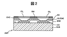
図2は、本発明の実施例2を説明する断面図である。図2では図1に示したカラーフィルタ材料インクINKは図示を省略した。実施例2のTFT基板AMPは、ガラス基板SUBの主面に、第1電極である陰極CD、バンクBNK、有機発光層OLE(W)、及び第2電極である透明陽極ADをこの順に形成する工程までは実施例1と同様である。実施例2では、透明陽極ADの上面に有機材料を塗布し、当該透明陽極ADを覆う層間膜OVCを形成して、バンクBNK等で生じた透明陽極ADの上面(換言すれば、有機発光層OLE(W)からの光の出射面)の起伏を均す。これにより、透明陽極ADの表面は平坦化される。この層間膜OVCは金属アルコキシド類を用いる。金属アルコキシドの層間膜OVCを平坦化する程度の膜厚以上(望ましくは、1μm以上)にスピン塗布し、オゾンと窒素の混合雰囲気中でUV照射を行って酸化性を向上させ、低温(望ましくは、100℃以下)で硬化する。 FIG. 2 is a sectional view for explaining a second embodiment of the present invention. In FIG. 2, the color filter material ink INK shown in FIG. 1 is not shown. In the TFT substrate AMP of Example 2, the cathode CD as the first electrode, the bank BNK, the organic light emitting layer OLE (W), and the transparent anode AD as the second electrode are formed in this order on the main surface of the glass substrate SUB. The process is the same as in Example 1. In Example 2, an organic material is applied to the upper surface of the transparent anode AD to form an interlayer film OVC that covers the transparent anode AD, and the upper surface of the transparent anode AD generated in the bank BNK or the like (in other words, an organic light emitting layer) The undulation of the light exit surface from OLE (W) is leveled. Thereby, the surface of the transparent anode AD is flattened. This interlayer film OVC uses metal alkoxides. The metal alkoxide interlayer film OVC is spin-coated to a thickness that is flat enough (preferably 1 μm or more), and UV irradiation is performed in a mixed atmosphere of ozone and nitrogen to improve the oxidization property. , 100 ° C. or lower).
その後、マスクを用いたスクリーン印刷で、画素間すなわちバンクBNKの直上部分に遮光層(ブラックマトリクス)BMを形成する。そして、ブラックマトリクスBMの開口にインクジェット装置のノズルからカラーフィルタ材料インクを滴下してカラーフィルタFILを形成する。 Thereafter, a light shielding layer (black matrix) BM is formed between pixels, that is, directly above the bank BNK by screen printing using a mask. Then, the color filter material ink is dropped from the nozzles of the ink jet device into the openings of the black matrix BM to form the color filter FIL.
なお、金属アルコキシドの層間膜OVCをオゾンと窒素の混合雰囲気中で処理する工程は処理時間の短縮のために採用するオプションであり、必須ではない。 Note that the process of processing the metal alkoxide interlayer film OVC in a mixed atmosphere of ozone and nitrogen is an option employed to shorten the processing time and is not essential.
カラーフィルタFILの形成後、当該カラーフィルタFILを透光性を有するガラス板あるいは可撓性フィルムなどの封止部材で覆い、周囲を封止して周囲環境からの湿気の侵入等による動作特性の劣化を防止し安定した表示を可能にする。 After the color filter FIL is formed, the color filter FIL is covered with a sealing member such as a light-transmitting glass plate or a flexible film, and the surroundings are sealed to provide operating characteristics due to moisture intrusion from the surrounding environment. Prevents deterioration and enables stable display.
実施例2によれば、実施例1の効果に加えて、有機EL発光層の平坦性が画素間で均一化でき、層間膜OVCの屈折率、ブラックマトリクスBMによる画素開口部の寸法を適宜に選択することで、隣接画素からの光漏れを防止でき、コントラスト、高色純度の画像表示を得ることができる。なお、実施例2についても、実施例1と同様のトップカソード構成とすることもできる。 According to the second embodiment, in addition to the effects of the first embodiment, the flatness of the organic EL light emitting layer can be made uniform between the pixels, and the refractive index of the interlayer film OVC and the size of the pixel opening by the black matrix BM are appropriately set. By selecting, light leakage from adjacent pixels can be prevented, and an image display with contrast and high color purity can be obtained. Note that the top cathode configuration similar to that of the first embodiment can be adopted in the second embodiment.
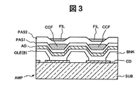
図3は、本発明の実施例3を説明する断面図である。実施例3には図1に示したカラーフィルタ材料インクINKは図示を省略した。実施例3のTFT基板AMPは、ガラス基板SUBの主面に形成した第1電極である陰極CD、バンクBNKの形成までは実施例1および実施例2と同様である。実施例3では、実施例1および実施例2における白色発光の有機発光層OLE(W)に代えて青色を発光する有機発光層OLE(B)をバンクBNKと陰極CDの開口部を覆って形成する。なお、実施例3のバンクBNKの高さは、実施例1および実施例2のそれよりも高く形成するのが望ましい。 FIG. 3 is a cross-sectional view for explaining a third embodiment of the present invention. In Example 3, the color filter material ink INK shown in FIG. 1 is not shown. The TFT substrate AMP of Example 3 is the same as that of Example 1 and Example 2 until the formation of the cathode CD and the bank BNK, which are the first electrodes formed on the main surface of the glass substrate SUB. In Example 3, instead of the organic light emitting layer OLE (W) emitting white light in Example 1 and Example 2, an organic light emitting layer OLE (B) that emits blue light is formed so as to cover the openings of the bank BNK and the cathode CD. To do. The height of the bank BNK of the third embodiment is desirably higher than that of the first and second embodiments.
次に、有機発光層OLE(B)の全面を覆って第2電極である陽極ADを形成し、陽極ADの上層に第1の保護層PAS1を成膜する。第1の保護層PAS1の上層で、バンクBNKで形成された凹部にインクジェット装置のノズルから波長変換フィルタ(青色光を3色のそれぞれの色に変換する色変換フィルタ)の材料インクを滴下して3色(R,G,B)の波長変換フィルタCCFを形成する。図3には二色の波長変換フィルタの塗布のみを示す。色変換フィルタCCFは、製造工程を短縮する上で3色夫々への波長変換に関与するフィルタ層の全てを同時に形成することが望ましいが、これは必要条件ではない。バンクBNKは、ノズルから滴下される波長変換フィルタ材料インク同士が混ざるのを抑止する。なお、青(B)の画素には波長変換フィルタを塗布しない構成も可能である。 Next, the anode AD as the second electrode is formed so as to cover the entire surface of the organic light emitting layer OLE (B), and the first protective layer PAS1 is formed on the anode AD. The material ink of the wavelength conversion filter (color conversion filter that converts blue light into each of the three colors) is dropped from the nozzles of the inkjet device into the recesses formed in the bank BNK on the upper layer of the first protective layer PAS1. A three-color (R, G, B) wavelength conversion filter CCF is formed. FIG. 3 shows only application of a two-color wavelength conversion filter. In order to shorten the manufacturing process, the color conversion filter CCF desirably forms all of the filter layers involved in wavelength conversion into three colors at the same time, but this is not a necessary condition. The bank BNK prevents the wavelength conversion filter material inks dropped from the nozzles from being mixed. A configuration in which a wavelength conversion filter is not applied to the blue (B) pixel is also possible.
波長変換フィルタCCFを覆って層間膜としても機能する第2の保護層PAS2を成膜する。この第2の保護層PAS2も第1の保護層PAS1と同様に、窒化シリコン(SiN)、または酸化シリコン(SiO)を用いるが、他の同様な材料、例えばアモルファスカーボン膜をプラズマCVDまたはスパッタリングで形成して用いることもできる。プラズマCVDで成膜したカーボン膜はダイアモンドライクな硬質膜となる。 A second protective layer PAS2 that covers the wavelength conversion filter CCF and also functions as an interlayer film is formed. Similarly to the first protective layer PAS1, the second protective layer PAS2 uses silicon nitride (SiN) or silicon oxide (SiO), but other similar materials such as an amorphous carbon film are formed by plasma CVD or sputtering. It can also be formed and used. The carbon film formed by plasma CVD becomes a diamond-like hard film.
次に、バンクBNKの表面形状を反映した第2の保護層PAS2の凹部にインクジェット装置のノズルからカラーフィルタ材料インクを滴下して3色(R,G,B)のカラーフィルタFILを形成する。図3には二色のカラーフィルタの塗布のみを示す。カラーフィルタFILは、製造工程を短縮する上で3色夫々の光を透過するフィルタ層の全てを同時に形成することが望ましいが、これは必要条件ではない。バンクBNKは、ノズルから滴下されるカラーフィルタ材料インク同士が混ざるのを抑止する。なお、青(B)の画素にはカラーフィルタを塗布しない構成も可能である。 Next, the color filter material ink is dropped from the nozzles of the ink jet device into the recesses of the second protective layer PAS2 reflecting the surface shape of the bank BNK to form the three color (R, G, B) color filters FIL. FIG. 3 shows only the application of two color filters. In order to shorten the manufacturing process, the color filter FIL desirably forms all the filter layers that transmit light of each of the three colors at the same time, but this is not a necessary condition. The bank BNK prevents the color filter material inks dropped from the nozzles from being mixed. A configuration in which a color filter is not applied to the blue (B) pixel is also possible.
カラーフィルタFILの形成後、当該カラーフィルタFILの上面を透光性を有するガラス板あるいは可撓性フィルムなどの封止部材で覆い、周囲を封止して周囲環境からの湿気の侵入等による動作特性の劣化を防止し安定した表示を可能にする。 After the formation of the color filter FIL, the upper surface of the color filter FIL is covered with a sealing member such as a light-transmitting glass plate or a flexible film, and the periphery is sealed to operate by intrusion of moisture from the surrounding environment. Prevents deterioration of characteristics and enables stable display.
実施例3によれば、現状では白色発光の有機発光層OLE(W)よりも高輝度かつ長寿命の青色を発光する有機発光層OLE(B)を用いることで、高輝度、高コントラストの画像表示を得ることができる。なお、実施例3についても、実施例1や実施例2と同様のトップカソード構成とすることもできる。 According to Example 3, by using the organic light emitting layer OLE (B) that emits blue light with higher luminance and longer life than the organic light emitting layer OLE (W) that emits white light at present, an image with high luminance and high contrast can be obtained. An indication can be obtained. Note that the top cathode configuration similar to that in the first and second embodiments can be employed in the third embodiment.
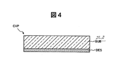
図4は、本発明の有機EL表示装置を構成するTFT基板AMPのカラーフィルタの形成面を封止する封止部材の一例を説明する模式断面図である。この封止部材CVPはガラス板SLSの内面に吸湿剤(乾燥剤)DESを設けてあり、図示しない周縁でTFT基板AMPに封止して有機EL表示装置(パネル)を完成する。 FIG. 4 is a schematic cross-sectional view illustrating an example of a sealing member that seals the color filter forming surface of the TFT substrate AMP constituting the organic EL display device of the present invention. This sealing member CVP is provided with a hygroscopic agent (desiccant) DES on the inner surface of the glass plate SLS, and is sealed to the TFT substrate AMP at a peripheral edge (not shown) to complete an organic EL display device (panel).
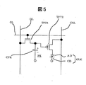
図5は、有機EL表示装置の画素の構成例を説明する回路図である。この画素PXはカラー表示では副画素(サブピクセル)となる。画素PXは、走査線GLとデータ線DLに接続したスイッチング用の薄膜トランジスタTFT1、走査線GLで選択されたスイッチング用薄膜トランジスタTFT1のオンでデータ線DLから供給される表示データを電荷として蓄積する蓄積容量CPR、有機EL素子OLEの駆動用薄膜トランジスタTFT2、電流供給線CSLで構成される。 FIG. 5 is a circuit diagram illustrating a configuration example of a pixel of the organic EL display device. This pixel PX becomes a sub-pixel (sub-pixel) in color display. The pixel PX has a storage capacitor that stores display data supplied from the data line DL as electric charges when the switching thin film transistor TFT1 connected to the scanning line GL and the data line DL is turned on and the switching thin film transistor TFT1 selected by the scanning line GL is turned on. It comprises a CPR, a driving thin film transistor TFT2 of the organic EL element OLE, and a current supply line CSL.
薄膜トランジスタTFT1のゲート電極は走査線GLに、ドレイン電極はデータ線DLに接続されている。また、薄膜トランジスタTFT2のゲート電極は薄膜トランジスタTFT1のソース電極に接続され、この接続点に蓄積容量CPRの一方の電極(+極)が接続されている。薄膜トランジスタTFT2のドレイン電極は電流供給線CSLに、ソース電極は有機EL素子OLEDの陽極ADに接続されている。 The gate electrode of the thin film transistor TFT1 is connected to the scanning line GL, and the drain electrode is connected to the data line DL. The gate electrode of the thin film transistor TFT2 is connected to the source electrode of the thin film transistor TFT1, and one electrode (+ electrode) of the storage capacitor CPR is connected to this connection point. The drain electrode of the thin film transistor TFT2 is connected to the current supply line CSL, and the source electrode is connected to the anode AD of the organic EL element OLED.
画素PXが走査線GLで選択されて薄膜トランジスタTFT1がオンとなると、データ線DLから供給される表示データが蓄積容量CPRに蓄積される。そして、薄膜トランジスタTFT1がオフした時点で薄膜トランジスタTFT2がオンとなり、電流供給線CSLから有機EL素子OLEDに流れ、ほぼ1フレームの期間(または、1フィールド期間)にわたってこの電流を持続させる。このとき流れる電流は、蓄積容量CPRに蓄積されているデータ信号に対応する電荷で規定される。ここ回路は最も単純な構成であり、他に種々の回路構成が知られている。 When the pixel PX is selected by the scanning line GL and the thin film transistor TFT1 is turned on, the display data supplied from the data line DL is stored in the storage capacitor CPR. When the thin film transistor TFT1 is turned off, the thin film transistor TFT2 is turned on and flows from the current supply line CSL to the organic EL element OLED, and this current is maintained for a period of almost one frame (or one field period). The current flowing at this time is defined by the charge corresponding to the data signal stored in the storage capacitor CPR. This circuit has the simplest configuration, and various other circuit configurations are known.
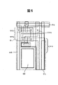
図6は、図5に示した画素の回路を基板上で実現した構成例を説明する画素付近の平面図である。図中、図5と同一の符号は同一部分に対応し、DEは画素の開口部である。薄膜トランジスタTFT1と薄膜トランジスタTFT2は画素の開口部DEに隣接する非表示部に配置される。 FIG. 6 is a plan view in the vicinity of a pixel for explaining a configuration example in which the circuit of the pixel shown in FIG. 5 is realized on a substrate. In the figure, the same reference numerals as those in FIG. 5 correspond to the same parts, and DE is a pixel opening. The thin film transistors TFT1 and TFT2 are arranged in a non-display portion adjacent to the pixel opening DE.
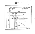
図7は、有機EL表示装置の駆動回路を含めた等価回路である。画素PXはマトリクス状に配列されて表示領域ARを形成する。データ線DLはデータ線駆動回路DDRにより駆動される。また、走査線GLは走査線駆動回路GDRで駆動される。電流供給線CSLは電流供給バスラインCSLBを介して図示しない電流供給回路に接続している。なお、TMは外部入力端子を示す。 FIG. 7 is an equivalent circuit including a drive circuit of the organic EL display device. The pixels PX are arranged in a matrix to form a display area AR. The data line DL is driven by the data line driving circuit DDR. The scanning line GL is driven by the scanning line driving circuit GDR. The current supply line CSL is connected to a current supply circuit (not shown) via a current supply bus line CSLB. TM denotes an external input terminal.
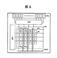
図8は、フルカラー表示の有機EL表示装置の構成を説明する等価回路である。3色の表示部R、G、Bのそれぞれは図7に示した画素(副画素)PXで構成され、走査線GL方向に配列されて1カラー画素(R、G、Bの各副画素PXで構成)を形成する。他の構成は図7と同様である。 FIG. 8 is an equivalent circuit illustrating the configuration of a full-color organic EL display device. Each of the three color display portions R, G, and B is composed of the pixels (sub-pixels) PX shown in FIG. 7, and is arranged in the direction of the scanning line GL so that each color pixel (R, G, and B sub-pixels PX). To form). Other configurations are the same as those in FIG.
異なるカラーフィルタ、あるいは異なる波長変換フィルタの材料をインクジェット装置を用いることで、高精度の塗布を実現し、隣接する画素に混色をもたらさないようにする効果は、有機EL表示装置に限らず、他の表示装置、例えばプラズマ素子を用いた表示装置などにも適用しても同様である。 By using an inkjet device with different color filters or different wavelength conversion filter materials, the effect of realizing high-precision coating and preventing color mixture in adjacent pixels is not limited to organic EL display devices, The same applies to other display devices such as a display device using a plasma element.
AMP・・・TFT基板、SUB・・・絶縁性の基板(ガラス基板)、CD・・・第1電極(陰極)、BNK・・・隔壁提(バンク)、OLE・・・有機発光層、OLE(W)・・・ 白色発光の有機発光層、AD・・・第2電極である透明陽極、PAS・・・保護層、IK・・・カラーフィルタ材料インク、FIL・・・カラーフィルタ、CCF・・・波長変換フィルタ。
AMP ... TFT substrate, SUB ... Insulating substrate (glass substrate), CD ... First electrode (cathode), BNK ... Partition wall (bank), OLE ... Organic light emitting layer, OLE (W) ... white light emitting organic light emitting layer, AD ... transparent anode as second electrode, PAS ... protective layer, IK ... color filter material ink, FIL ... color filter, CCF. ..Wavelength conversion filter
Claims (20)
前記第2電極の上部には前記有機EL層から発せられた白色光を所定の色に変換するカラーフィルタが湿式工程で塗布され、
前記第2電極と前記カラーフィルタとの間に、該カラーフィルタの塗布材料による前記有機EL層の劣化を防止するための保護層を設けたことを特徴とする有機EL表示装置。 A plurality of organic EL light emitting elements disposed in a main surface of the substrate, each of the organic EL light emitting elements including one of a plurality of first electrodes formed on the main surface of the substrate and the plurality of first electrodes; An organic EL layer that covers the electrodes in common and has white light-emitting ability; and a second electrode that is formed on the organic EL layer and is commonly formed in the plurality of organic EL light-emitting elements. An organic EL display device that emits the emitted light to the second electrode side,
A color filter that converts white light emitted from the organic EL layer into a predetermined color is applied on the second electrode by a wet process,
An organic EL display device, wherein a protective layer is provided between the second electrode and the color filter to prevent the deterioration of the organic EL layer due to the color filter coating material.
前記隔壁堤に形成され且つ前記第1電極を露出する該隔壁堤の凹部内において、前記有機EL発光層は該第1電極に接していることを特徴とする請求項1に記載の有機EL表示装置。 Each of the plurality of first electrodes is separated from the others of the plurality of first electrodes adjacent thereto by a bulkhead bank having a thickness greater than that of the first electrode surrounding the periphery.
2. The organic EL display according to claim 1, wherein the organic EL light emitting layer is in contact with the first electrode in a recess of the partition wall formed on the partition wall and exposing the first electrode. apparatus.
前記第2電極の上に、当該第2電極の表面を平坦にする平坦化層が設けられており、
前記平坦化層の上部には、前記有機EL層から発せられた白色光を所定の色に変換するカラーフィルタが湿式工程での塗布により前記有機EL発光素子毎に形成されていることを特徴とする有機EL表示装置。 A plurality of organic EL light emitting elements disposed in a main surface of the substrate, each of the organic EL light emitting elements including one of a plurality of first electrodes formed on the main surface of the substrate and the plurality of first electrodes; An organic EL layer that covers the electrodes in common and has white light-emitting ability; and a second electrode that is formed on the organic EL layer and is commonly formed in the plurality of organic EL light-emitting elements. An organic EL display device that emits the emitted light to the second electrode side,
A planarizing layer is provided on the second electrode to flatten the surface of the second electrode,
A color filter that converts white light emitted from the organic EL layer into a predetermined color is formed on the planarization layer for each organic EL light emitting element by application in a wet process. Organic EL display device.
前記隔壁堤に形成され且つ前記第1電極を露出する該隔壁堤の凹部内において、前記有機EL発光層は該第1電極に接していることを特徴とする請求項8に記載の有機EL表示装置。 Each of the plurality of first electrodes is separated from the others of the plurality of first electrodes adjacent thereto by a bulkhead bank having a thickness greater than that of the first electrode surrounding the periphery.
9. The organic EL display according to claim 8, wherein the organic EL light emitting layer is in contact with the first electrode in a recess of the partition wall formed on the partition wall and exposing the first electrode. apparatus.
前記第2電極の上部には、前記有機EL層から発せられた光の波長を所定の波長に変換する波長変換フィルタが前記有機EL発光素子毎に湿式工程における塗布で形成され、
前記波長変換フィルタの各々の上部には、当該波長変換フィルタを通した光を所定の色に変換する波長変換フィルタが前記有機EL発光素子毎に湿式工程における塗布で形成され、
前記第2電極と前記波長変換フィルタの間に、該波長変換フィルタの塗布材料による前記有機EL層の劣化を防止するための第1の保護層が設けられ、
前記波長変換フィルタと前記カラーフィルタの間に、該カラーフィルタの塗布材料による前記有機EL層の劣化を防止するための第2の保護層が設けられていることを特徴とする有機EL表示装置。 A plurality of organic EL light emitting elements disposed in a main surface of the substrate, each of the organic EL light emitting elements including one of a plurality of first electrodes formed on the main surface of the substrate and the plurality of first electrodes; An organic EL layer that covers the electrodes in common and has white light-emitting ability; and a second electrode that is formed on the organic EL layer and is commonly formed in the plurality of organic EL light-emitting elements. An organic EL display device that emits the emitted light to the second electrode side,
A wavelength conversion filter that converts the wavelength of light emitted from the organic EL layer to a predetermined wavelength is formed on the second electrode by coating in a wet process for each organic EL light emitting element.
A wavelength conversion filter that converts light that has passed through the wavelength conversion filter into a predetermined color is formed on each of the wavelength conversion filters by application in a wet process for each organic EL light emitting element,
Between the second electrode and the wavelength conversion filter, a first protective layer for preventing deterioration of the organic EL layer due to the coating material of the wavelength conversion filter is provided,
An organic EL display device, wherein a second protective layer for preventing deterioration of the organic EL layer due to a coating material of the color filter is provided between the wavelength conversion filter and the color filter.
前記隔壁堤に形成され且つ前記第1電極を露出する該隔壁堤の凹部内には、該第1電極の上面に接する前記有機EL発光層が形成されていることを特徴とする請求項14に記載の有機EL表示装置。 Each of the plurality of first electrodes is separated from the others of the plurality of first electrodes adjacent thereto by a bulkhead bank having a thickness greater than that of the first electrode surrounding the periphery.
The organic EL light emitting layer in contact with the upper surface of the first electrode is formed in a concave portion of the partition wall formed on the partition wall and exposing the first electrode. The organic EL display device described.
The organic EL display device according to claim 19, wherein a hygroscopic agent is provided in the inside sealed by the sealing member.
Priority Applications (3)
| Application Number | Priority Date | Filing Date | Title |
|---|---|---|---|
| JP2004206105A JP2006032010A (en) | 2004-07-13 | 2004-07-13 | Organic EL display device |
| US11/178,421 US7893607B2 (en) | 2004-07-13 | 2005-07-12 | Organic electroluminescence display device |
| CNA2005100840166A CN1722925A (en) | 2004-07-13 | 2005-07-12 | Organic electroluminescence display device |
Applications Claiming Priority (1)
| Application Number | Priority Date | Filing Date | Title |
|---|---|---|---|
| JP2004206105A JP2006032010A (en) | 2004-07-13 | 2004-07-13 | Organic EL display device |
Publications (2)
| Publication Number | Publication Date |
|---|---|
| JP2006032010A true JP2006032010A (en) | 2006-02-02 |
| JP2006032010A5 JP2006032010A5 (en) | 2007-04-26 |
Family
ID=35598750
Family Applications (1)
| Application Number | Title | Priority Date | Filing Date |
|---|---|---|---|
| JP2004206105A Pending JP2006032010A (en) | 2004-07-13 | 2004-07-13 | Organic EL display device |
Country Status (3)
| Country | Link |
|---|---|
| US (1) | US7893607B2 (en) |
| JP (1) | JP2006032010A (en) |
| CN (1) | CN1722925A (en) |
Cited By (25)
| Publication number | Priority date | Publication date | Assignee | Title |
|---|---|---|---|---|
| JP2007234391A (en) * | 2006-03-01 | 2007-09-13 | Seiko Epson Corp | ELECTROLUMINESCENT DISPLAY DEVICE AND ELECTRONIC DEVICE |
| JP2008066216A (en) * | 2006-09-11 | 2008-03-21 | Seiko Epson Corp | ORGANIC ELECTROLUMINESCENT DEVICE, ITS MANUFACTURING METHOD, AND ELECTRONIC DEVICE |
| JP2008277270A (en) * | 2007-03-30 | 2008-11-13 | Dainippon Printing Co Ltd | Light-emitting organic EL display panel |
| JP2009020493A (en) * | 2007-06-13 | 2009-01-29 | Canon Inc | Organic light emitting panel |
| WO2010013637A1 (en) * | 2008-07-29 | 2010-02-04 | 富士電機ホールディングス株式会社 | Color conversion organic el display |
| WO2011061789A1 (en) | 2009-11-17 | 2011-05-26 | 富士電機ホールディングス株式会社 | Organic el display |
| JP2012028058A (en) * | 2010-07-21 | 2012-02-09 | Seiko Epson Corp | Organic electroluminescent device, method for manufacturing organic electroluminescent device, and electronic equipment |
| US8304265B2 (en) | 2007-09-19 | 2012-11-06 | Sharp Kabushiki Kaisha | Color conversion filter and manufacturing method of the organic EL display |
| US8520331B2 (en) | 2009-02-16 | 2013-08-27 | Sharp Kabushiki Kaisha | Color conversion filter manufacturing method |
| KR20140031004A (en) * | 2012-09-04 | 2014-03-12 | 삼성디스플레이 주식회사 | Organic light emitting display apparatus and method of manufacturing thereof |
| JP2014511019A (en) * | 2011-04-11 | 2014-05-01 | コミッサリア ア レネルジ アトミック エ オー エネルジ アルターネイティブス | Organic optoelectronic device and sealing method thereof |
| JP2014103424A (en) * | 2014-03-10 | 2014-06-05 | Sharp Corp | Organic el display |
| JP2014116128A (en) * | 2012-12-07 | 2014-06-26 | Japan Display Inc | Organic el display device |
| US8766299B2 (en) | 2010-05-21 | 2014-07-01 | Seiko Epson Corporation | Electro-optical device and electronic apparatus comprising electro-optical device having color filter and sealing film |
| JP2015026508A (en) * | 2013-07-26 | 2015-02-05 | 株式会社ジャパンディスプレイ | Light emitting element display device |
| JP2015103406A (en) * | 2013-11-25 | 2015-06-04 | 株式会社ジャパンディスプレイ | Organic EL display device |
| JP2015128003A (en) * | 2013-12-27 | 2015-07-09 | ソニー株式会社 | Display device and electronic device |
| JP2015156381A (en) * | 2015-03-31 | 2015-08-27 | ユニファイド イノヴェイティヴ テクノロジー, エルエルシー | Organic electroluminescence (el) display |
| US9620569B2 (en) | 2014-07-25 | 2017-04-11 | Seiko Epson Corporation | Light-emitting device and electronic apparatus |
| US9666646B2 (en) | 2013-10-10 | 2017-05-30 | Seiko Epson Corporation | Light emitting element disposed in a display region of a substrate |
| JP2017120758A (en) * | 2015-12-28 | 2017-07-06 | 三星ディスプレイ株式會社Samsung Display Co.,Ltd. | Organic light-emitting display device and method for manufacturing the same |
| KR20170079626A (en) * | 2015-12-30 | 2017-07-10 | 엘지디스플레이 주식회사 | White light emitting device and hybrid display device using the same |
| KR20180099997A (en) * | 2017-02-28 | 2018-09-06 | 한국생산기술연구원 | Quantum dot hybrid organic light emitting display device and method for manufacturing the same |
| KR20210118292A (en) * | 2020-03-19 | 2021-09-30 | 삼성디스플레이 주식회사 | Display apparatus |
| JP2025038003A (en) * | 2016-08-10 | 2025-03-18 | 株式会社半導体エネルギー研究所 | Method for manufacturing a display device |
Families Citing this family (21)
| Publication number | Priority date | Publication date | Assignee | Title |
|---|---|---|---|---|
| TWI491303B (en) * | 2009-06-29 | 2015-07-01 | 群創光電股份有限公司 | Image display system |
| JP5452178B2 (en) * | 2009-11-12 | 2014-03-26 | 株式会社日立ハイテクノロジーズ | Vacuum deposition apparatus, vacuum deposition method, and organic EL display device manufacturing method |
| JP5677435B2 (en) * | 2010-08-06 | 2015-02-25 | パナソニック株式会社 | Organic EL display panel and manufacturing method thereof |
| KR101784994B1 (en) * | 2011-03-31 | 2017-10-13 | 삼성디스플레이 주식회사 | Organic light emitting diode display and manufacturing method thereof |
| CN103797531A (en) * | 2012-09-10 | 2014-05-14 | 深圳市柔宇科技有限公司 | Large-size display screen and manufacturing method therefor |
| US9024336B2 (en) * | 2013-05-28 | 2015-05-05 | J Touch Corporation | Display panel driven by electrode wires |
| KR20150010232A (en) * | 2013-07-18 | 2015-01-28 | 삼성디스플레이 주식회사 | Organic light emitting display apparatus and method of manufacturing the same |
| KR20150019325A (en) * | 2013-08-13 | 2015-02-25 | 삼성디스플레이 주식회사 | Organic light emitting diode display and method for preparing the same |
| CN107004699A (en) * | 2014-12-18 | 2017-08-01 | Lg电子株式会社 | Organic LED display device |
| TWI557486B (en) * | 2014-12-31 | 2016-11-11 | 鴻海精密工業股份有限公司 | Thin film transistor substrate, manufacturing method thereof and display panel |
| CN111627924B (en) * | 2016-06-14 | 2023-05-16 | 群创光电股份有限公司 | Display device and method for manufacturing display device |
| KR102831200B1 (en) * | 2017-02-02 | 2025-07-10 | 서울반도체 주식회사 | Light emitting diode package |
| KR20190033979A (en) * | 2017-09-22 | 2019-04-01 | 주식회사 루멘스 | vertical type light emitting elements having color conversion electrode part |
| CN111512701B (en) * | 2017-12-26 | 2023-07-21 | 堺显示器制品株式会社 | Organic EL device and manufacturing method thereof |
| US11088348B2 (en) * | 2018-01-31 | 2021-08-10 | Sakai Display Products Corporation | Method for producing organic electroluminescent display device comprising polydiacetylene layer |
| CN111630938A (en) * | 2018-01-31 | 2020-09-04 | 堺显示器制品株式会社 | Organic EL display device and method of manufacturing the same |
| CN110164910B (en) * | 2018-05-28 | 2021-04-23 | 京东方科技集团股份有限公司 | Color conversion layer and preparation method thereof, and display device |
| KR102747738B1 (en) * | 2018-11-09 | 2025-01-02 | 삼성디스플레이 주식회사 | Display device and method of manufacturing of the same |
| KR102901601B1 (en) | 2019-10-08 | 2025-12-18 | 삼성디스플레이 주식회사 | Display device |
| KR102870085B1 (en) | 2019-10-11 | 2025-10-17 | 삼성디스플레이 주식회사 | Color-converting substrate, display device including the same and method for manufacturing the same |
| KR20220021978A (en) * | 2020-08-14 | 2022-02-23 | 삼성디스플레이 주식회사 | Display device |
Citations (3)
| Publication number | Priority date | Publication date | Assignee | Title |
|---|---|---|---|---|
| JPH10162958A (en) * | 1996-11-28 | 1998-06-19 | Casio Comput Co Ltd | EL element |
| JP2003142256A (en) * | 2001-11-07 | 2003-05-16 | Futaba Corp | Organic EL device |
| WO2003069957A1 (en) * | 2002-02-12 | 2003-08-21 | Idemitsu Kosan Co., Ltd. | Organic el display and its production method |
Family Cites Families (6)
| Publication number | Priority date | Publication date | Assignee | Title |
|---|---|---|---|---|
| JP2850820B2 (en) * | 1995-02-09 | 1999-01-27 | 株式会社デンソー | EL element |
| US6140766A (en) * | 1997-12-27 | 2000-10-31 | Hokuriku Electric Industry Co., Ltd. | Organic EL device |
| JP4472120B2 (en) * | 2000-06-08 | 2010-06-02 | 東北パイオニア株式会社 | Organic electroluminescence device and method for manufacturing the same |
| JP4011292B2 (en) * | 2001-01-15 | 2007-11-21 | 株式会社日立製作所 | LIGHT EMITTING ELEMENT AND DISPLAY DEVICE |
| JP2003234186A (en) * | 2001-12-06 | 2003-08-22 | Sony Corp | Display device and method of manufacturing the same |
| JP2004031215A (en) | 2002-06-27 | 2004-01-29 | Toyota Industries Corp | Color display device |
-
2004
- 2004-07-13 JP JP2004206105A patent/JP2006032010A/en active Pending
-
2005
- 2005-07-12 CN CNA2005100840166A patent/CN1722925A/en active Pending
- 2005-07-12 US US11/178,421 patent/US7893607B2/en active Active
Patent Citations (3)
| Publication number | Priority date | Publication date | Assignee | Title |
|---|---|---|---|---|
| JPH10162958A (en) * | 1996-11-28 | 1998-06-19 | Casio Comput Co Ltd | EL element |
| JP2003142256A (en) * | 2001-11-07 | 2003-05-16 | Futaba Corp | Organic EL device |
| WO2003069957A1 (en) * | 2002-02-12 | 2003-08-21 | Idemitsu Kosan Co., Ltd. | Organic el display and its production method |
Cited By (54)
| Publication number | Priority date | Publication date | Assignee | Title |
|---|---|---|---|---|
| JP2007234391A (en) * | 2006-03-01 | 2007-09-13 | Seiko Epson Corp | ELECTROLUMINESCENT DISPLAY DEVICE AND ELECTRONIC DEVICE |
| JP2008066216A (en) * | 2006-09-11 | 2008-03-21 | Seiko Epson Corp | ORGANIC ELECTROLUMINESCENT DEVICE, ITS MANUFACTURING METHOD, AND ELECTRONIC DEVICE |
| JP2008277270A (en) * | 2007-03-30 | 2008-11-13 | Dainippon Printing Co Ltd | Light-emitting organic EL display panel |
| JP2009020493A (en) * | 2007-06-13 | 2009-01-29 | Canon Inc | Organic light emitting panel |
| US8446091B2 (en) | 2007-09-19 | 2013-05-21 | Sharp Kabushiki Kaisha | Color conversion filter and manufacturing method of the organic EL display |
| US8304265B2 (en) | 2007-09-19 | 2012-11-06 | Sharp Kabushiki Kaisha | Color conversion filter and manufacturing method of the organic EL display |
| WO2010013637A1 (en) * | 2008-07-29 | 2010-02-04 | 富士電機ホールディングス株式会社 | Color conversion organic el display |
| JP2010033905A (en) * | 2008-07-29 | 2010-02-12 | Fuji Electric Holdings Co Ltd | Color conversion system organic el display |
| US8044575B2 (en) | 2008-07-29 | 2011-10-25 | Fuji Electric Co., Ltd. | Color conversion type organic EL display |
| KR101266345B1 (en) * | 2008-07-29 | 2013-05-22 | 샤프 가부시키가이샤 | Color conversion organic el display |
| US8520331B2 (en) | 2009-02-16 | 2013-08-27 | Sharp Kabushiki Kaisha | Color conversion filter manufacturing method |
| JP5791514B2 (en) * | 2009-11-17 | 2015-10-07 | ユニファイド イノヴェイティヴ テクノロジー, エルエルシー | Organic EL display |
| US9929370B2 (en) | 2009-11-17 | 2018-03-27 | Unified Innovative Technology, Llc | Organic EL display |
| WO2011061789A1 (en) | 2009-11-17 | 2011-05-26 | 富士電機ホールディングス株式会社 | Organic el display |
| US8766299B2 (en) | 2010-05-21 | 2014-07-01 | Seiko Epson Corporation | Electro-optical device and electronic apparatus comprising electro-optical device having color filter and sealing film |
| JP2012028058A (en) * | 2010-07-21 | 2012-02-09 | Seiko Epson Corp | Organic electroluminescent device, method for manufacturing organic electroluminescent device, and electronic equipment |
| JP2014511019A (en) * | 2011-04-11 | 2014-05-01 | コミッサリア ア レネルジ アトミック エ オー エネルジ アルターネイティブス | Organic optoelectronic device and sealing method thereof |
| KR20140031004A (en) * | 2012-09-04 | 2014-03-12 | 삼성디스플레이 주식회사 | Organic light emitting display apparatus and method of manufacturing thereof |
| KR101980233B1 (en) * | 2012-09-04 | 2019-05-21 | 삼성디스플레이 주식회사 | Organic light emitting display apparatus and method of manufacturing thereof |
| JP2014116128A (en) * | 2012-12-07 | 2014-06-26 | Japan Display Inc | Organic el display device |
| JP2015026508A (en) * | 2013-07-26 | 2015-02-05 | 株式会社ジャパンディスプレイ | Light emitting element display device |
| US9666646B2 (en) | 2013-10-10 | 2017-05-30 | Seiko Epson Corporation | Light emitting element disposed in a display region of a substrate |
| JP2015103406A (en) * | 2013-11-25 | 2015-06-04 | 株式会社ジャパンディスプレイ | Organic EL display device |
| US9577018B2 (en) | 2013-12-27 | 2017-02-21 | Sony Corporation | Display unit and electronic apparatus |
| JP2015128003A (en) * | 2013-12-27 | 2015-07-09 | ソニー株式会社 | Display device and electronic device |
| US12207505B2 (en) | 2013-12-27 | 2025-01-21 | Sony Group Corporation | Display unit and electronic apparatus |
| US11937468B2 (en) | 2013-12-27 | 2024-03-19 | Sony Group Corporation | Display unit and electronic apparatus |
| US10263061B2 (en) | 2013-12-27 | 2019-04-16 | Sony Corporation | Display unit and electronic apparatus |
| US9991325B2 (en) | 2013-12-27 | 2018-06-05 | Sony Corporation | Display unit and electronic apparatus |
| US11659739B2 (en) | 2013-12-27 | 2023-05-23 | Sony Group Corporation | Display unit and electronic apparatus |
| US11024694B2 (en) | 2013-12-27 | 2021-06-01 | Sony Corporation | Display unit and electronic apparatus |
| JP2014103424A (en) * | 2014-03-10 | 2014-06-05 | Sharp Corp | Organic el display |
| US9620569B2 (en) | 2014-07-25 | 2017-04-11 | Seiko Epson Corporation | Light-emitting device and electronic apparatus |
| JP2015156381A (en) * | 2015-03-31 | 2015-08-27 | ユニファイド イノヴェイティヴ テクノロジー, エルエルシー | Organic electroluminescence (el) display |
| JP2017120758A (en) * | 2015-12-28 | 2017-07-06 | 三星ディスプレイ株式會社Samsung Display Co.,Ltd. | Organic light-emitting display device and method for manufacturing the same |
| KR102444177B1 (en) * | 2015-12-28 | 2022-09-19 | 삼성디스플레이 주식회사 | Organic light emitting display device and manufacturing method thereof |
| US10825871B2 (en) | 2015-12-28 | 2020-11-03 | Samsung Display Co., Ltd. | Organic light-emitting display apparatus and method of manufacturing the same |
| US10879317B2 (en) | 2015-12-28 | 2020-12-29 | Samsung Display Co., Ltd. | Organic light-emitting display apparatus and method of manufacturing the same |
| KR102845513B1 (en) | 2015-12-28 | 2025-08-12 | 삼성디스플레이 주식회사 | Organic light emitting display apparatus |
| KR20240096430A (en) * | 2015-12-28 | 2024-06-26 | 삼성디스플레이 주식회사 | Organic light emitting display apparatus |
| US11342388B2 (en) | 2015-12-28 | 2022-05-24 | Samsung Display Co., Ltd. | Organic light-emitting display apparatus comprising quantum dots |
| US12120936B2 (en) | 2015-12-28 | 2024-10-15 | Samsung Display Co., Ltd. | Organic light-emitting display apparatus and method of manufacturing the same |
| KR20220127793A (en) * | 2015-12-28 | 2022-09-20 | 삼성디스플레이 주식회사 | Organic light emitting display apparatus |
| KR20170077929A (en) * | 2015-12-28 | 2017-07-07 | 삼성디스플레이 주식회사 | Organic light emitting display apparatus and method for manufacturing the same |
| US11737336B2 (en) | 2015-12-28 | 2023-08-22 | Samsung Display Co., Ltd. | Organic light-emitting display apparatus comprising quantum dots |
| KR102667850B1 (en) * | 2015-12-28 | 2024-05-23 | 삼성디스플레이 주식회사 | Organic light emitting display apparatus |
| KR20170079626A (en) * | 2015-12-30 | 2017-07-10 | 엘지디스플레이 주식회사 | White light emitting device and hybrid display device using the same |
| KR102609507B1 (en) * | 2015-12-30 | 2023-12-04 | 엘지디스플레이 주식회사 | White light emitting device and hybrid display device using the same |
| JP2025038003A (en) * | 2016-08-10 | 2025-03-18 | 株式会社半導体エネルギー研究所 | Method for manufacturing a display device |
| KR20180099997A (en) * | 2017-02-28 | 2018-09-06 | 한국생산기술연구원 | Quantum dot hybrid organic light emitting display device and method for manufacturing the same |
| KR101965157B1 (en) * | 2017-02-28 | 2019-04-08 | 한국생산기술연구원 | Quantum dot hybrid organic light emitting display device and method for manufacturing the same |
| WO2018160018A3 (en) * | 2017-02-28 | 2018-10-25 | 한국생산기술연구원 | Hybrid quantum dot organic light emitting display device and manufacturing method therefor |
| KR20210118292A (en) * | 2020-03-19 | 2021-09-30 | 삼성디스플레이 주식회사 | Display apparatus |
| KR102787866B1 (en) * | 2020-03-19 | 2025-04-01 | 삼성디스플레이 주식회사 | Display apparatus |
Also Published As
| Publication number | Publication date |
|---|---|
| US20060012288A1 (en) | 2006-01-19 |
| US7893607B2 (en) | 2011-02-22 |
| CN1722925A (en) | 2006-01-18 |
Similar Documents
| Publication | Publication Date | Title |
|---|---|---|
| US7893607B2 (en) | Organic electroluminescence display device | |
| JP5459142B2 (en) | ORGANIC EL DEVICE, METHOD FOR MANUFACTURING ORGANIC EL DEVICE, AND ELECTRONIC DEVICE | |
| KR101980233B1 (en) | Organic light emitting display apparatus and method of manufacturing thereof | |
| US7696681B2 (en) | Stacked organic electroluminescent units for white light emission provided with RGB color conversion portions | |
| KR100944311B1 (en) | Light emitting element and display device using this light emitting element | |
| JP6514679B2 (en) | Organic light emitting diode display | |
| US7309957B2 (en) | Organic electroluminescent display device and method of fabricating the same | |
| KR102491876B1 (en) | Display apparutus | |
| KR20150042367A (en) | Organic electro luminescent device and method of fabricating the same | |
| KR102409702B1 (en) | Organic Light Emitting Diode Display Device | |
| US11714515B2 (en) | Display device | |
| JP2005031251A (en) | Light-emitting display device | |
| JP2002299044A (en) | Electroluminescence display device | |
| JP2011090925A (en) | Method for manufacturing electro-optical device | |
| CN114664890A (en) | Display device | |
| CN114725163A (en) | Display device | |
| WO2019176457A1 (en) | Organic el display device and method for manufacturing organic el display device | |
| EP2197061B1 (en) | Organic light emitting diode display | |
| JP2007026852A (en) | ORGANIC ELECTROLUMINESCENT DEVICE, METHOD FOR PRODUCING ORGANIC ELECTROLUMINESCENT DEVICE, AND ELECTRONIC DEVICE | |
| JP4858054B2 (en) | LIGHT EMITTING DEVICE AND ELECTRONIC DEVICE | |
| JP4729754B2 (en) | Display device using a plurality of organic EL light emitting elements | |
| JP2011009093A (en) | Organic el device and electronic equipment | |
| JP2006338946A (en) | Display panel | |
| CN113658979A (en) | Electro-optical device and electronic apparatus | |
| KR20150033406A (en) | Organic electro-luminescent device and methode of fabricating the same |
Legal Events
| Date | Code | Title | Description |
|---|---|---|---|
| A521 | Request for written amendment filed |
Free format text: JAPANESE INTERMEDIATE CODE: A523 Effective date: 20070306 |
|
| A621 | Written request for application examination |
Free format text: JAPANESE INTERMEDIATE CODE: A621 Effective date: 20070306 |
|
| A977 | Report on retrieval |
Free format text: JAPANESE INTERMEDIATE CODE: A971007 Effective date: 20100128 |
|
| A131 | Notification of reasons for refusal |
Free format text: JAPANESE INTERMEDIATE CODE: A131 Effective date: 20100309 |
|
| A521 | Request for written amendment filed |
Free format text: JAPANESE INTERMEDIATE CODE: A523 Effective date: 20100430 |
|
| A131 | Notification of reasons for refusal |
Free format text: JAPANESE INTERMEDIATE CODE: A131 Effective date: 20100622 |
|
| A711 | Notification of change in applicant |
Free format text: JAPANESE INTERMEDIATE CODE: A712 Effective date: 20110218 |
|
| RD03 | Notification of appointment of power of attorney |
Free format text: JAPANESE INTERMEDIATE CODE: A7423 Effective date: 20110218 |
|
| A02 | Decision of refusal |
Free format text: JAPANESE INTERMEDIATE CODE: A02 Effective date: 20110816 |