JP2006038457A - Film probe manufacturing method - Google Patents
Film probe manufacturing method Download PDFInfo
- Publication number
- JP2006038457A JP2006038457A JP2004213869A JP2004213869A JP2006038457A JP 2006038457 A JP2006038457 A JP 2006038457A JP 2004213869 A JP2004213869 A JP 2004213869A JP 2004213869 A JP2004213869 A JP 2004213869A JP 2006038457 A JP2006038457 A JP 2006038457A
- Authority
- JP
- Japan
- Prior art keywords
- layer
- insulating resin
- resin layer
- plating
- support substrate
- Prior art date
- Legal status (The legal status is an assumption and is not a legal conclusion. Google has not performed a legal analysis and makes no representation as to the accuracy of the status listed.)
- Pending
Links
- 238000004519 manufacturing process Methods 0.000 title claims abstract description 31
- 239000000523 sample Substances 0.000 title claims abstract description 29
- 239000010410 layer Substances 0.000 claims abstract description 230
- 229920005989 resin Polymers 0.000 claims abstract description 80
- 239000011347 resin Substances 0.000 claims abstract description 80
- 238000007747 plating Methods 0.000 claims abstract description 64
- 239000000758 substrate Substances 0.000 claims abstract description 64
- 229910052751 metal Inorganic materials 0.000 claims abstract description 58
- 239000002184 metal Substances 0.000 claims abstract description 58
- 230000015572 biosynthetic process Effects 0.000 claims abstract description 10
- 239000002344 surface layer Substances 0.000 claims abstract description 3
- 238000005530 etching Methods 0.000 claims description 31
- RYGMFSIKBFXOCR-UHFFFAOYSA-N Copper Chemical group [Cu] RYGMFSIKBFXOCR-UHFFFAOYSA-N 0.000 claims description 23
- 229910052802 copper Inorganic materials 0.000 claims description 23
- 239000010949 copper Substances 0.000 claims description 23
- 239000000463 material Substances 0.000 claims description 10
- 229910000881 Cu alloy Inorganic materials 0.000 claims description 3
- 239000004065 semiconductor Substances 0.000 abstract description 5
- 239000010408 film Substances 0.000 description 30
- 238000000034 method Methods 0.000 description 27
- 239000011295 pitch Substances 0.000 description 17
- 239000012790 adhesive layer Substances 0.000 description 16
- 229920001721 polyimide Polymers 0.000 description 13
- 239000009719 polyimide resin Substances 0.000 description 12
- 239000007864 aqueous solution Substances 0.000 description 10
- 239000011241 protective layer Substances 0.000 description 9
- 239000000243 solution Substances 0.000 description 9
- PXHVJJICTQNCMI-UHFFFAOYSA-N Nickel Chemical compound [Ni] PXHVJJICTQNCMI-UHFFFAOYSA-N 0.000 description 8
- 230000001681 protective effect Effects 0.000 description 8
- 239000002585 base Substances 0.000 description 7
- QGZKDVFQNNGYKY-UHFFFAOYSA-N Ammonia Chemical compound N QGZKDVFQNNGYKY-UHFFFAOYSA-N 0.000 description 6
- 239000004020 conductor Substances 0.000 description 6
- 238000009713 electroplating Methods 0.000 description 6
- 239000011521 glass Substances 0.000 description 6
- 238000007689 inspection Methods 0.000 description 6
- 239000004973 liquid crystal related substance Substances 0.000 description 6
- VHUUQVKOLVNVRT-UHFFFAOYSA-N Ammonium hydroxide Chemical compound [NH4+].[OH-] VHUUQVKOLVNVRT-UHFFFAOYSA-N 0.000 description 5
- 239000000853 adhesive Substances 0.000 description 5
- 230000001070 adhesive effect Effects 0.000 description 5
- 235000011114 ammonium hydroxide Nutrition 0.000 description 5
- 230000000873 masking effect Effects 0.000 description 5
- 229920001225 polyester resin Polymers 0.000 description 5
- 239000004645 polyester resin Substances 0.000 description 5
- NLXLAEXVIDQMFP-UHFFFAOYSA-N Ammonium chloride Substances [NH4+].[Cl-] NLXLAEXVIDQMFP-UHFFFAOYSA-N 0.000 description 4
- 229910052759 nickel Inorganic materials 0.000 description 4
- 239000010935 stainless steel Substances 0.000 description 4
- 229910001220 stainless steel Inorganic materials 0.000 description 4
- 239000010409 thin film Substances 0.000 description 4
- 229910021578 Iron(III) chloride Inorganic materials 0.000 description 3
- HEMHJVSKTPXQMS-UHFFFAOYSA-M Sodium hydroxide Chemical compound [OH-].[Na+] HEMHJVSKTPXQMS-UHFFFAOYSA-M 0.000 description 3
- -1 aliphatic amino alcohol Chemical class 0.000 description 3
- 229910000365 copper sulfate Inorganic materials 0.000 description 3
- ARUVKPQLZAKDPS-UHFFFAOYSA-L copper(II) sulfate Chemical compound [Cu+2].[O-][S+2]([O-])([O-])[O-] ARUVKPQLZAKDPS-UHFFFAOYSA-L 0.000 description 3
- 230000000694 effects Effects 0.000 description 3
- 239000003822 epoxy resin Substances 0.000 description 3
- RBTARNINKXHZNM-UHFFFAOYSA-K iron trichloride Chemical compound Cl[Fe](Cl)Cl RBTARNINKXHZNM-UHFFFAOYSA-K 0.000 description 3
- 238000010030 laminating Methods 0.000 description 3
- KERTUBUCQCSNJU-UHFFFAOYSA-L nickel(2+);disulfamate Chemical compound [Ni+2].NS([O-])(=O)=O.NS([O-])(=O)=O KERTUBUCQCSNJU-UHFFFAOYSA-L 0.000 description 3
- 229920003223 poly(pyromellitimide-1,4-diphenyl ether) Polymers 0.000 description 3
- 229920000647 polyepoxide Polymers 0.000 description 3
- 238000003825 pressing Methods 0.000 description 3
- 238000004544 sputter deposition Methods 0.000 description 3
- XEEYBQQBJWHFJM-UHFFFAOYSA-N Iron Chemical compound [Fe] XEEYBQQBJWHFJM-UHFFFAOYSA-N 0.000 description 2
- 229910000990 Ni alloy Inorganic materials 0.000 description 2
- 239000004642 Polyimide Substances 0.000 description 2
- 238000010521 absorption reaction Methods 0.000 description 2
- 229910052783 alkali metal Inorganic materials 0.000 description 2
- 150000001340 alkali metals Chemical class 0.000 description 2
- 238000004140 cleaning Methods 0.000 description 2
- ORTQZVOHEJQUHG-UHFFFAOYSA-L copper(II) chloride Chemical compound Cl[Cu]Cl ORTQZVOHEJQUHG-UHFFFAOYSA-L 0.000 description 2
- 230000001186 cumulative effect Effects 0.000 description 2
- 239000000835 fiber Substances 0.000 description 2
- 229920006259 thermoplastic polyimide Polymers 0.000 description 2
- 229920005992 thermoplastic resin Polymers 0.000 description 2
- 229920001187 thermosetting polymer Polymers 0.000 description 2
- 238000007740 vapor deposition Methods 0.000 description 2
- 229910052782 aluminium Inorganic materials 0.000 description 1
- XAGFODPZIPBFFR-UHFFFAOYSA-N aluminium Chemical compound [Al] XAGFODPZIPBFFR-UHFFFAOYSA-N 0.000 description 1
- 229910021529 ammonia Inorganic materials 0.000 description 1
- 239000000908 ammonium hydroxide Substances 0.000 description 1
- 238000007664 blowing Methods 0.000 description 1
- 238000005266 casting Methods 0.000 description 1
- 239000000919 ceramic Substances 0.000 description 1
- 239000003795 chemical substances by application Substances 0.000 description 1
- KRVSOGSZCMJSLX-UHFFFAOYSA-L chromic acid Substances O[Cr](O)(=O)=O KRVSOGSZCMJSLX-UHFFFAOYSA-L 0.000 description 1
- 229960003280 cupric chloride Drugs 0.000 description 1
- 238000000151 deposition Methods 0.000 description 1
- 230000008021 deposition Effects 0.000 description 1
- 239000000428 dust Substances 0.000 description 1
- 238000007772 electroless plating Methods 0.000 description 1
- 238000000866 electrolytic etching Methods 0.000 description 1
- 239000011888 foil Substances 0.000 description 1
- AWJWCTOOIBYHON-UHFFFAOYSA-N furo[3,4-b]pyrazine-5,7-dione Chemical group C1=CN=C2C(=O)OC(=O)C2=N1 AWJWCTOOIBYHON-UHFFFAOYSA-N 0.000 description 1
- 229910052742 iron Inorganic materials 0.000 description 1
- 230000001678 irradiating effect Effects 0.000 description 1
- 238000003475 lamination Methods 0.000 description 1
- 239000007788 liquid Substances 0.000 description 1
- 238000000465 moulding Methods 0.000 description 1
- 238000000206 photolithography Methods 0.000 description 1
- 229920000728 polyester Polymers 0.000 description 1
- 230000001105 regulatory effect Effects 0.000 description 1
- 235000011121 sodium hydroxide Nutrition 0.000 description 1
Images


Landscapes
- Testing Or Measuring Of Semiconductors Or The Like (AREA)
- Measuring Leads Or Probes (AREA)
Abstract
Description
本発明は、狭小なピッチの端子を有する半導体や表示装置等の検査に用いるのに好適なフィルムプローブの製造方法に関する。 The present invention relates to a method of manufacturing a film probe suitable for use in inspection of a semiconductor having a narrow pitch terminal, a display device or the like.
従来周知のように、半導体等の検査に際し、半導体等(被検査体側)と検査装置側とを導通させる為の手段として、二ードル型プローブもしくはL字ピン型プローブが使用されている。これらのプローブは、ニードルもしくはピンを精度良く組み立てなければならなく、高度な熟練度と多大な作業工数を必要とする。その為、被検査体の端子ピッチが、およそ100μm以下の狭小ピッチである場合や、同時に検査すべき端子数が数百以上といったように多い場合においては非常に高価になり、更に、数十μm以下の狭小ピッチの場合においては、それの製造が非常に難しいといった欠点を有している。 As is well known in the art, a needle type probe or an L-shaped pin type probe is used as a means for conducting a semiconductor or the like (inspected object side) and the inspection apparatus side when inspecting a semiconductor or the like. These probes must assemble needles or pins with high accuracy, and require a high degree of skill and a great number of work steps. For this reason, when the terminal pitch of the object to be inspected is a narrow pitch of about 100 μm or less, or when the number of terminals to be inspected is large, such as several hundred or more, it becomes very expensive, and furthermore, several tens of μm. The following narrow pitches have the disadvantage that they are very difficult to manufacture.
そこで、それらに代えて、可撓性の絶縁樹脂層に接触子を設けた一般にフィルムプローブと呼ばれているものが既に提案されており、かかるフィルムプローブの製造方法の一例が下記特許文献1に記載されている。この公知の製造方法は、一面に導電性金属層を積層した可撓性の絶縁樹脂層を用意し、該導電性金属層を配線回路および/もしくはランドにパターン加工する。 Therefore, instead of them, what is generally called a film probe in which a contact is provided on a flexible insulating resin layer has already been proposed, and an example of a method for manufacturing such a film probe is disclosed in Patent Document 1 below. Are listed. In this known manufacturing method, a flexible insulating resin layer having a conductive metal layer laminated on one surface is prepared, and the conductive metal layer is patterned into a wiring circuit and / or a land.
次いで、該絶縁樹脂層、配線回路および/もしくはランドの必要箇所に保護絶縁樹脂層を積層し、次いで、該保護絶縁樹脂層に開孔を形成した後、該配線回路を陰極として該開孔内に導電性金属をめっき形成し、よって、めっき形成された導電性金属が該保護絶縁樹脂層の一面に達して等方的に拡がって半球状の接触子を形成するものである。 Next, a protective insulating resin layer is laminated at a necessary portion of the insulating resin layer, the wiring circuit and / or the land, and then an opening is formed in the protective insulating resin layer, and then the wiring circuit is used as a cathode in the opening. Then, the conductive metal is formed by plating, and the conductive metal thus formed reaches one surface of the protective insulating resin layer and isotropically spreads to form a hemispherical contact.
なお、保護絶縁層に開孔を設けることに代えて、絶縁樹脂層に開孔を設け、該開孔内に導電性金属をめっき成長させて絶縁樹脂層表面に接触子を形成することもできるが、この方法によればフォトリソグラフィ技術やレーザー加工技術を利用することができ、接触子のピッチが100μm以下と狭小であっても、また、数百又は数千を超える接触子数であっても容易に製造することができる。 Instead of providing an opening in the protective insulating layer, an opening can be provided in the insulating resin layer, and a conductive metal can be plated and grown in the opening to form a contact on the surface of the insulating resin layer. However, according to this method, a photolithography technique or a laser processing technique can be used, and even if the contact pitch is as narrow as 100 μm or less, the number of contacts exceeds several hundreds or thousands. Can also be manufactured easily.
しかし、この方法で製造したフィルムプローブは、接触子や配線回路等をめっきおよび/もしくはエッチングによって絶縁樹脂層や保護絶縁樹脂層に形成する工程中に、温度や吸湿の程度によって絶縁樹脂層や保護絶縁樹脂層自体が伸縮を繰り返すため、形成される接触子や配線回路等の位置が、用いたガラスマスクやレーザー加工時のそれに対しておよそ±0.05%程度ずれるという欠点があった。 However, the film probe manufactured by this method is not suitable for the insulating resin layer and the protective layer depending on the temperature and the degree of moisture absorption during the process of forming the contactor and the wiring circuit on the insulating resin layer and the protective insulating resin layer by plating and / or etching. Since the insulating resin layer itself repeatedly expands and contracts, there is a drawback that the position of the formed contactor, wiring circuit, etc. is shifted by about ± 0.05% with respect to the glass mask used or that during laser processing.
また、この製造法においては、接触子の高さはめっき成長速度に左右されるから、かかる速度を一定に制御しなければならないが、実際上、めっき槽内の場所による電流密度のむら等によってめっき速度のむらが避けられないために接触子高さのむらが生じやすいといった欠点もあった。 In this manufacturing method, since the height of the contact depends on the plating growth speed, it is necessary to control the speed constantly. However, in practice, the plating is caused by uneven current density depending on the location in the plating tank. There is also a disadvantage that unevenness of the contact is likely to occur because unevenness in speed is inevitable.
また、他のフィルムプローブの製造方法として、ベース基板上に絶縁樹脂層を積層形成し、該絶縁樹脂層に開口部を形成し、該開口部内に導体電極(接触子)を形成し、該導体電極および該絶縁樹脂層上に第2絶縁樹脂層を形成し、該第2絶縁樹脂層上に導体薄膜層を形成し、該導体薄膜層上に配線パターン状の第2開口部を形成し、該第2開口部内に配線回路を形成し、該配線回路および該第2絶縁樹脂層上に第3絶縁樹脂層を形成し、続いて、該ベース基板および該絶縁樹脂層および導体薄膜層の不要部分を除去してフィルムプローブを得る方法が提案されている(特許文献2参照)。 As another method of manufacturing a film probe, an insulating resin layer is laminated on a base substrate, an opening is formed in the insulating resin layer, a conductor electrode (contact) is formed in the opening, and the conductor Forming a second insulating resin layer on the electrode and the insulating resin layer; forming a conductive thin film layer on the second insulating resin layer; forming a second opening in a wiring pattern on the conductive thin film layer; A wiring circuit is formed in the second opening, a third insulating resin layer is formed on the wiring circuit and the second insulating resin layer, and then the base substrate, the insulating resin layer, and the conductive thin film layer are not required. There has been proposed a method of obtaining a film probe by removing a portion (see Patent Document 2).
この製造方法によれば、位置精度が高く、高さむらが小さい導体電極(接触子)を持つフィルムプローブを得ることができる。しかし、この製造方法によるフィルムプローブは導体電極(接触子)および配線回路が絶縁樹脂層表層に、その底面および絶縁樹脂層に埋設された側面を把持されて構成されており、狭小ピッチの場合には、その把持面積が小さくなり、従って、把持力が小さくなるため、検査を繰り返して行う際の押圧力やクリーニングのための拭き拭いによる引き剥がし力等によって導体電極(接触子)や配線回路が破損や浮き上がりを起こしやすいと言う欠点があった。 According to this manufacturing method, it is possible to obtain a film probe having a conductor electrode (contactor) with high positional accuracy and small height unevenness. However, the film probe according to this manufacturing method is configured such that the conductor electrode (contactor) and the wiring circuit are gripped on the surface of the insulating resin layer and the bottom surface and the side surface embedded in the insulating resin layer. Since the gripping area is small and the gripping force is small, the conductor electrode (contactor) and the wiring circuit are connected by the pressing force when the inspection is repeated and the peeling force by wiping for cleaning. There was a drawback that it was easily damaged and lifted.
また、その製造工程において、ベース基板と絶縁樹脂層を剥離する際に、絶縁樹脂層に殆ど変形を起こさない程度の十分に小さい力で剥離する必要があり、そのためには、ベース基板と絶縁樹脂層とを好適な接着強度で積層形成することが重要であるが、実際上、接着強度を好適な大きさに制御することが難しく、大き過ぎる場合には、ベース基板と絶縁樹脂層を剥離する際に、絶縁樹脂層が変形し、結果として、導体電極(接触子)の位置精度が悪くなったり、また逆に小さすぎる場合には、製造工程中にベース基板と絶縁樹脂層が剥離するトラブルの原因となったりすると言う欠点があった。 In the manufacturing process, when the base substrate and the insulating resin layer are peeled off, it is necessary to peel off the insulating resin layer with a sufficiently small force that hardly causes deformation of the insulating resin layer. It is important to form a layer with a suitable adhesive strength, but in practice it is difficult to control the adhesive strength to a suitable size. If it is too large, the base substrate and the insulating resin layer are peeled off. When the insulating resin layer is deformed, as a result, the position accuracy of the conductor electrode (contactor) is deteriorated, or conversely, if it is too small, the base substrate and the insulating resin layer are peeled off during the manufacturing process. There was a drawback that it might cause.
本発明は、上述の欠点に鑑みて発明されたものであって、その目的は、狭小なピッチで多数の端子を持つ半導体や表示装置の検査に用いるのに好適なフィルムプローブを製造する方法を提供することである。 The present invention has been invented in view of the above-described drawbacks, and its object is to provide a method for manufacturing a film probe suitable for use in inspection of a semiconductor or display device having a large number of terminals at a narrow pitch. Is to provide.
上述の目的を達成するための本発明のフィルムプローブの製造方法は、表面に支持基板めっき層を形成した支持基板と一面に導電性金属層を有する絶縁樹脂層とを、該支持基板めっき層が内層側に、また、該導電性金属層が表層側となるように積層した積層体の、該導電性金属層及び該絶縁樹脂層に設けられた金属層開孔および電極体形成用開孔内に電極体をめっき形成し、その後、該積層体から該支持基板を、続いて該支持基板めっき層を除去し、次に、該絶縁樹脂層をハーフエッチングして該絶縁樹脂層の表面に該電極体の一部を突出せしめて接触子となすことを特徴としている。 In order to achieve the above-mentioned object, the film probe manufacturing method of the present invention comprises: a support substrate having a support substrate plating layer formed on a surface; and an insulating resin layer having a conductive metal layer on one surface. In the laminated body laminated on the inner layer side so that the conductive metal layer is on the surface layer side, the metal layer opening provided in the conductive metal layer and the insulating resin layer and the opening for forming the electrode body Then, the support substrate and then the support substrate plating layer are removed from the laminate, and then the insulating resin layer is half-etched to form the electrode on the surface of the insulating resin layer. A feature is that a part of the electrode body protrudes to form a contact.
本発明の方法により得られるフィルムプローブは、温度や吸湿の程度による寸法変化が実質的に殆どない支持基板を巧に利用して、接触子を電解めっき法等によって形成するようにしているために、接触子同士間ピッチ等の寸法精度を一段と高めることがでると共に、接触子の高さが、絶縁樹脂層の厚さによって規制されるために、接触子の高さむらを小さくすることができる。 Since the film probe obtained by the method of the present invention makes good use of a support substrate that has substantially no dimensional change due to temperature and the degree of moisture absorption, the contact is formed by electrolytic plating or the like. In addition, it is possible to further increase the dimensional accuracy such as the pitch between the contacts, and the height of the contacts is regulated by the thickness of the insulating resin layer, so that the unevenness of the height of the contacts can be reduced. .
また、本発明の製造方法においては、積層体から支持基板及び支持基板めっき層を取り除くに際し、まず、支持基板と支持基板めっき層の間で剥離し、ついで、支持基板めっき層はエッチング処理によって除くため、支持基板として例えば表面をバフ研磨等で鏡面状に仕上げたステンレス板や表面をクロム酸処理したステンレス板等を用いるか、めっき剥離剤を利用することによって、絶縁樹脂層等に過大な力をかけることなく支持基板と支持基板めっき層の間で剥離することができる。 In the production method of the present invention, when removing the support substrate and the support substrate plating layer from the laminate, first, the support substrate and the support substrate plating layer are peeled off, and then the support substrate plating layer is removed by an etching process. For this reason, for example, a stainless steel plate whose surface is mirror-finished by buffing or the like, a stainless steel plate whose surface is chromic acid-treated, or the like is used as a support substrate, or a plating release agent is used, so that excessive force is applied to the insulating resin layer, etc. It can peel between a support substrate and a support substrate plating layer, without applying.
本発明の製造方法によれば、狭小なピッチであっても、接触子のピッチ精度および高さ精度が高い、かつ、検査を繰り返すことによる押圧力やクリーニングのための吹き払いによる引き剥がし力等により接触子や電極パッドや配線回路に破損や剥がれが起こる恐れが少ないフィルムプローブを容易に製造することが出来る。 According to the manufacturing method of the present invention, even with a narrow pitch, the contact pitch accuracy and height accuracy are high, the pressing force by repeating the inspection, the peeling force by blowing for cleaning, etc. This makes it possible to easily manufacture a film probe that is less likely to cause damage or peeling to the contactor, electrode pad, or wiring circuit.
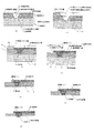
本発明による製造方法の一例について図1、図2、図5を用いて説明する。まず、支持基板3の表面に支持基板めっき層31を設けた導電性支持基板11と絶縁樹脂層1の表面に導電性金属層2を設けた回路基材12を、支持基板めっき層31が内層側に、導電性金属層2が外層側となるように積層し、次に、絶縁樹脂層1および導電性金属層2の所定の位置に互いに連なる電極形成用開孔42及び金属層開孔21を設けて、積層体10を準備する(図1(a)参照)。
An example of the manufacturing method according to the present invention will be described with reference to FIGS. First, the support
絶縁樹脂層1としては、電気的、熱的、機械的特性等を勘案してポリイミド樹脂や液晶ポリエステル樹脂が好適に用いられ、また、導電性金属層2としては銅が好適に用いられるが、それぞれ他の材質であっても良い。
As the insulating resin layer 1, a polyimide resin or a liquid crystal polyester resin is preferably used in consideration of electrical, thermal, mechanical characteristics, and the
絶縁樹脂層1表面に導電性金属層2を設ける方法としては、導電性金属箔上に絶縁樹脂層を流延して成形する方法、絶縁樹脂層表面にスパッタ処理、蒸着処理、無電解めっき処理等によって金属シード層を形成した後に導電性金属層をめっき形成する方法や、接着剤層を介して絶縁樹脂層と導電性金属層を積層する方法等が利用できる。
As a method of providing the
絶縁樹脂層1の厚さは、後に電極体形成用開孔42内に形成される電極体41の高さに対応し、およそ12〜150μmの範囲が好適に用いられる。また、導電性金属層2は、後にエッチング処理され、その一部が電極パッド下層51や配線回路下層61となり、その厚さは1〜10μmが好適に用いられるが、それぞれ、必ずしもこの範囲に限定されるものではない。
The thickness of the insulating resin layer 1 corresponds to the height of the
一方、支持基板3としてはステンレス、銅、アルミニウム、鉄等の金属板が好適に用いられるが、セラミックやガラス等の表面にスパッタや蒸着処理等によって金属薄膜を形成して導電性を付与したものであってもよい。支持基板3の表面にはスルファミン酸ニッケル浴によるニッケルめっきや硫酸銅めっき浴による銅めっき等によって支持基板めっき層31が形成されている。支持基板めっき層31の厚さはおよそ1μmから10μmの厚さが用いられるが、必ずしもその範囲に限定されるものではない。
On the other hand, a metal plate made of stainless steel, copper, aluminum, iron, or the like is preferably used as the
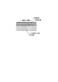
支持基板めっき層31の表面上に、片面に導電性金属層2を積層した絶縁樹脂層1を積層する方法としては、絶縁樹脂層1として液晶ポリエステル樹脂や熱可塑性ポリイミド樹脂等の熱可塑性樹脂を用いる場合には、加熱圧着することによって積層することができる。また、絶縁樹脂層1として熱硬化性ポリイミド樹脂等の非熱可塑性樹脂を用いる場合には、ポリイミド樹脂系やエポキシ樹脂系等の接着剤層9を介して加熱圧着することによって積層することができる(図5参照)。
As a method of laminating the insulating resin layer 1 in which the
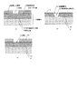
積層体10の絶縁樹脂層1および導電性金属層2にそれぞれ電極形成用開孔42、金属層開孔21を設ける方法の一例について、図2を用いて説明する。まず、上述した方法により得られる積層体10の導電性金属層2表面にドライフィルムレジストをラミネートし、所定のパターンを持つマスクを介して露光し、現像して所定の位置に開孔71を有するレジスト膜70を形成する(図2(a)参照)。続いて、導電性金属層2をエッチング処理することにより導電性金属層2に金属層開孔21を設ける(図2(b)参照)。かかるエッチング液としては、導電性金属層2が銅の場合には、塩化第2鉄やアンモニアの水溶液等が利用できる。ドライフィルムレジストに代えて液体レジストを用いても良い。
An example of a method of providing the electrode forming opening 42 and the metal layer opening 21 in the insulating resin layer 1 and the
次に、レジスト膜70を除去した後、金属層開孔21を設けた導電性金属層2をマスクとして利用して、絶縁樹脂層1をエッチング処理して支持基板めっき層31表面に達するブラインドビアホール状の電極形成用開孔42を形成する(図2(c)参照)。かかるエッチング液としては、絶縁樹脂層1がポリイミド樹脂もしくは液晶ポリエステル樹脂の場合には、アルカリ金属とエタノールジアミン等の脂肪族アミノアルコール誘導体を含む水溶液が好適に利用できる。
Next, after removing the resist film 70, the blind via hole reaching the surface of the support
支持基板めっき層31と絶縁樹脂層1との間に接着剤層9が介在する場合には上述したエッチング処理により絶縁樹脂層1に開孔を設けた後、更に、接着剤層9に対してエッチング活性を有する第2のエッチング液を用いてエッチング処理して支持基板めっき層31表面に達する電極形成用開孔42を形成する。接着剤層9がポリイミド系接着剤の場合には脂肪族アミノアルコール誘導体とアンモニウムヒドロキシドを含む水溶液が第2のエッチング液として好適に利用できる。
In the case where the adhesive layer 9 is interposed between the support
また、上述したエッチング処理に代えて金属層開孔21を有する導電性金属層2を利用してエキシマレーザーやUVレーザー等のレーザー光を照射して絶縁樹脂層1や接着剤層9に電極形成用開孔42を設けることもできる。また、レーザー光を照射して導電性金属層2および絶縁樹脂層1に直接開孔を形成することもできる。
Further, instead of the etching process described above, the
また、電極形成用開孔42内の支持基板めっき層31の表面に樹脂等が残存していると、後に電極形成用開孔42内に電極体を4めっき形成する際に、空洞等のめっき形成不良を起こす原因となるため、エッチング処理によって絶縁樹脂層1に電極形成用開孔42を設けた後に、レーザー光を照射して支持基板めっき層31表面の残存樹脂等の残査を取り除くことが有効である。
In addition, if resin or the like remains on the surface of the support
次に、上述した方法によって準備された積層体10の導電性金属層2の表面に、ドライフィルムレジストをラミネートし、所定のパターンを持つマスクを介して露光し、現像して電極形成用開孔42および金属層開孔21に連なる電極パッド上層形成用開孔53と、これに連なる配線回路上層形成用開孔63を有するレジスト膜80を形成する(図2(b)参照)。
Next, a dry film resist is laminated on the surface of the
次に、導電性支持基板11を陰極として、めっき浴中で電解めっきを行う。まず、支持基板めっき層31表面から電極体形成用開孔42内に電極体41がめっき形成され、電極体41が導電性金属層2に達すると導電性金属層2が陰極に導通されて、金属層開孔21内、パッド上層形成用開孔53内および配線回路上層形成用開孔63内にそれぞれ電極体41、電極パッド上層52および配線回路上層62が形成される(図1(c)参照)。電解めっき方法としてはスルファミン酸ニッケルめっき浴によるニッケルめっきや、硫酸銅めっき浴による銅めっき等が好適に用いられる。
Next, electrolytic plating is performed in a plating bath using the conductive support substrate 11 as a cathode. First, an
電極体形成用開孔42内に電極体41をめっき形成する際に、支持基板めっき層31および導電性金属層2の両者を陰極となして通電すると、電極体形成用開孔42及び金属層開孔21内に支持基板めっき層31と導電性金属層2の両方向からめっき形成されるため、電極体41内部に空隙が出来やすく、また導電性金属層2表面上に過剰の厚さの電極パッド上層52および配線回路上層62が形成されるため好ましくない。
When the
次に、苛性ソーダ水溶液等のアルカリ水溶液によりレジスト層80を除去した後、電極パッド上層52および配線回路上層62をマスクとして利用して、導電性金属層2の不要部分をエッチング除去し、絶縁樹脂層1上に電極パッド5および配線回路6を形成する(図1(d)参照)。
Next, after removing the resist layer 80 with an alkaline aqueous solution such as an aqueous solution of caustic soda, unnecessary portions of the
かかるエッチング処理を好適に行うには、電極体41や電極パッド上層52および配線回路上層62を形成するめっき材質として導電性金属層2の材質と異なる材質を選ぶことが好ましい。導電性金属層2の材質が銅もしくは銅合金で、めっき形成する電極パッド上層52および配線回路上層62の材質がニッケルもしくはニッケル合金の場合には、アンモニア水溶液が好適に利用できるが、導電性金属層2の厚さが電極パッド上層52や配線回路上層62の厚さに比較して十分小さい場合には塩化第2銅や塩化第2鉄の水溶液等を用いることもできる。電極体41等の材質は必ずしも一種類に限定されるものではなく、2種類以上の材質を積層して形成しても良い。
In order to perform such an etching process suitably, it is preferable to select a material different from the material of the
次に、支持基板3を支持基板めっき層31との間で剥離して取り除き(図1(e)参照)、続いて、支持基板めっき層31をエッチング処理して取り除く(図1(f)参照)。かかるエッチング液としては支持基板めっき層31にはエッチング活性があり、電極体41にはエッチング活性が殆ど無いか、もしくは小さいエッチング液が特に好適に利用でき、例えば、支持基板めっき層31の材質が銅または銅合金で、電極体41の材質がニッケルまたはニッケル合金の場合にはアンモニア水溶液が好適に利用できる。
Next, the
次に、絶縁樹脂層1をエッチング液でハーフエッチング処理して、電極体41の一部を絶縁樹脂層1表面上に突出させて接触子4を形成する(図1(g)参照)。かかるエッチング液としては絶縁樹脂層1の材質がポリイミド樹脂や液晶ポリエステルの場合には前述したアルカリ金属とエタノールジアミン等の脂肪族アミノアルコール誘導体を含む水溶液等が好適に用いられる。
Next, the insulating resin layer 1 is half-etched with an etching solution, and a part of the
可撓性絶縁樹脂層1表面上に突出する接触子4の高さは、被検査体電極周囲の保護層形成の有無や、保護層が形成されている場合にはその保護層の厚さ等によって異なるがおよそ2μmから50μmの範囲で好適に用いられる。 The height of the contact 4 protruding on the surface of the flexible insulating resin layer 1 is the presence or absence of the protective layer around the electrode to be inspected, the thickness of the protective layer if a protective layer is formed, etc. It is preferably used in the range of about 2 μm to 50 μm although it varies depending on the case.
なお、フィルムプローブにおいて、被検査体電極と導通を取るために繰り返し加えられる押圧力等によって接触子4等が破損や剥離することを防ぐために、また、埃が電極パッド5や配線回路6の間に付着して短絡することを防ぐために、絶縁樹脂層1上に電極パッド5および配線回路6を覆うように保護絶縁層8を設けることが有効である(図4参照)。 In the film probe, in order to prevent the contact 4 or the like from being damaged or peeled off due to a pressing force repeatedly applied to establish electrical connection with the electrode to be inspected, dust is generated between the electrode pad 5 and the wiring circuit 6. It is effective to provide a protective insulating layer 8 on the insulating resin layer 1 so as to cover the electrode pads 5 and the wiring circuit 6 (see FIG. 4).
かかる場合には、上述した図1(d)に示す工程の後に、絶縁樹脂層1や電極パッド5や配線回路6上に絶縁保護層8を積層する工程を加え(図3参照)、しかる後、前述した方法と同様の方法により、支持基板3、導電性めっき層31を順次取り除いて、次に絶縁樹脂層1をハーフエッチングして接触子4を形成して、フィルムプローブを製作することが出来る。
In such a case, after the step shown in FIG. 1 (d), a step of laminating the insulating protective layer 8 on the insulating resin layer 1, the electrode pad 5 and the wiring circuit 6 is added (see FIG. 3). The film probe can be manufactured by sequentially removing the
絶縁保護層8としてはポリイミド樹脂、液晶ポリエステル樹脂、繊維強化エポキシ樹脂等が好適に利用できる。絶縁保護層8が液晶ポリエステル樹脂、熱可塑性ポリイミド樹脂、繊維強化エポキシ樹脂等の場合には加熱圧着することで積層積層することができ、また熱硬化性ポリイミド樹脂の場合には着剤層を介して加熱圧着することによって積層することができる。保護層の厚さは5μmから100μmの範囲が好適に用いられるが、必ずしもこの範囲に限定されものではない。 As the insulating protective layer 8, polyimide resin, liquid crystal polyester resin, fiber reinforced epoxy resin, or the like can be suitably used. When the insulating protective layer 8 is a liquid crystal polyester resin, a thermoplastic polyimide resin, a fiber reinforced epoxy resin, etc., it can be laminated and laminated by thermocompression bonding. In the case of a thermosetting polyimide resin, the insulating protective layer 8 is interposed via an adhesive layer. Can be laminated by thermocompression bonding. The thickness of the protective layer is preferably in the range of 5 μm to 100 μm, but is not necessarily limited to this range.
上述した製造方法によるフィルムプローブには配線回路6が設けられているが、本発明に係る製造方法は、そのような配線回路を設けないていないフィルムプローブも製造できる。すなわち、絶縁樹脂層1の表面に突出して形成された接触端子4と、検査装置と導通接続するための電極パッド5を備えたフィルムプローブも上述した製造方法で製造することができる。 Although the wiring probe 6 is provided in the film probe by the manufacturing method described above, the manufacturing method according to the present invention can also manufacture a film probe not provided with such a wiring circuit. That is, the film probe provided with the contact terminal 4 protruding from the surface of the insulating resin layer 1 and the electrode pad 5 for conducting connection with the inspection apparatus can also be manufactured by the above-described manufacturing method.
なお、上述した電解めっきやエッチングを行う際に、適宜マスキングテープ等によるマスキング処理を行うことによって、不必要な個所へめっき析出やエッチングがなされることを防止することができる。 In addition, when performing the above-described electrolytic plating or etching, it is possible to prevent plating deposition or etching from being performed on unnecessary portions by appropriately performing a masking process using a masking tape or the like.
表面を鏡面状にバフ研磨した厚さ0.2mmのステンレス製の支持基板に硫酸銅メッキ浴中で銅メッキを行って、厚さおよそ5μmの支持基板めっき層を形成した。次に、前記支持基板めっき層表面に宇部興産社製ポリイミド樹脂系接着剤「UPA−8517C」をバーコーターで塗布し、熱風乾燥しておよそ5μm厚さの接着剤層を形成し、この上に、厚さ25μmの東レ・デュポン社製ポリイミドフィルム「カプトン」の片面に金属スパッタ薄層を介して電解めっきによって厚さ4μmの銅層を形成した絶縁樹脂層を、銅層が表面となるように積層して、圧力2MPa、最高温度180℃の条件で加熱圧着して積層体を得た。 A 0.2 mm-thick stainless steel support substrate whose surface was mirror-buffed was subjected to copper plating in a copper sulfate plating bath to form a support substrate plating layer having a thickness of approximately 5 μm. Next, a polyimide resin adhesive “UPA-8517C” manufactured by Ube Industries, Ltd. is applied to the surface of the support substrate plating layer with a bar coater and dried with hot air to form an adhesive layer having a thickness of about 5 μm. An insulating resin layer in which a copper layer having a thickness of 4 μm is formed on one side of a polyimide film “Kapton” made by Toray DuPont with a thickness of 25 μm by electroplating through a thin metal sputtering layer so that the copper layer becomes the surface. Lamination was performed by thermocompression bonding under conditions of a pressure of 2 MPa and a maximum temperature of 180 ° C. to obtain a laminate.
前記積層体の銅層表面上に日合・モートン社製ドライフィルムレジスト「NIT2025」(厚さ25μm)を加熱圧着してラミネートし、ピッチが90μmで、径がφ50μmのパターンをもつガラスマスクを介して、露光し、現像してピッチが90μmで、径がφ50μmの開孔を有するレジスト膜を形成した。次に塩化第2鉄水溶液中でエッチング処理して前記銅層にピッチが90μmで、径φ50μm、の銅層開孔を形成し、レジスト膜はアルカリ水溶液で剥離除去した。 A dry film resist “NIT2025” (thickness 25 μm) manufactured by Nichigo-Morton is laminated on the surface of the copper layer of the laminate by thermocompression bonding through a glass mask having a pattern with a pitch of 90 μm and a diameter of φ50 μm. Then, exposure and development were performed to form a resist film having openings with a pitch of 90 μm and a diameter of φ50 μm. Next, etching was performed in a ferric chloride aqueous solution to form copper layer openings having a pitch of 90 μm and a diameter of 50 μm in the copper layer, and the resist film was stripped and removed with an alkaline aqueous solution.
次に、前記銅層開孔を形成した銅層をマスクとして利用し、東レエンジニアリング社製ポリイミドエッチング液「TPE−3000」で「カプトン」層を、続いて同「TPE−ER10」で接着剤層をエッチング処理して、前記銅層開孔に連なり、支持基板めっき層表面に達する、その部分の径がおよそφ20μmのブラインドビアホール状の電極体形成用開孔を形成した。 Next, using the copper layer in which the copper layer opening is formed as a mask, a “Kapton” layer is formed with a polyimide etching solution “TPE-3000” manufactured by Toray Engineering Co., Ltd., and then an adhesive layer is formed with the same “TPE-ER10”. Was etched to form a blind via-hole-shaped opening for electrode body formation having a diameter of about 20 μm that continued to the copper layer opening and reached the surface of the support substrate plating layer.
次に、前記銅層開孔を形成した銅層の上に前記「NIT2025」を加熱圧着し、ガラスマスクを介して露光し、現像して、前記銅層開孔と同芯状のピッチが90μmで、径がφ55μmの電極パッド形成用開孔およびピッチ90μmで、幅が25μmの配線回路下層形成用開孔を有するレジスト膜を形成した。 Next, the “NIT2025” is thermocompression-bonded on the copper layer in which the copper layer openings are formed, exposed through a glass mask, developed, and a pitch concentric with the copper layer openings is 90 μm. Then, a resist film having electrode pad forming openings having a diameter of 55 μm and a wiring circuit lower layer forming opening having a pitch of 90 μm and a width of 25 μm was formed.
ついで、前記支持基板を陰極としてスルファミン酸ニッケルめっき浴中で電解めっきを行って、電極体形成用開孔内及び銅層開孔内に電極体をめっき形成し、続いて、電極パッド上層形成用開孔内および配線回路上層形成用開孔内にそれぞれ厚さがおよそ4μmの電極パッド上層および配線回路上層を銅層表面に形成した。その後、レジスト膜はアルカリ水溶液で剥離した。続いて、前記電極パッド上層および配線回路上層が表面上にめっき形成された銅層をアンモニア水溶液中でエッチング処理を行って、絶縁樹脂層表面に電極パッドおよび配線回路を形成した。 Next, electrolytic plating is performed in a nickel sulfamate plating bath using the support substrate as a cathode to form electrode bodies in the electrode body formation holes and in the copper layer openings, and subsequently for electrode pad upper layer formation. An electrode pad upper layer and a wiring circuit upper layer having a thickness of about 4 μm were formed on the surface of the copper layer in the opening and in the wiring circuit upper layer forming opening, respectively. Thereafter, the resist film was peeled off with an alkaline aqueous solution. Subsequently, the copper layer having the electrode pad upper layer and the wiring circuit upper layer plated thereon was etched in an aqueous ammonia solution to form the electrode pad and the wiring circuit on the surface of the insulating resin layer.
続いて、前記電極パッドおよび配線回路が形成された絶縁樹脂層表面に宇部興産社製ポリイミド樹脂系接着剤「UPA−8517C」を塗布し、乾燥させて厚さ5μmの接着剤層を形成し、その上に片面に厚さ5μmの前記接着剤層を形成した厚さ50μmの東レ・デュポン社製ポリイミド樹脂フィルム「カプトン」をそれぞれの接着剤層を合わせて積層し、圧力2MPa、温度180℃で加熱圧着して、支持基板、支持基板めっき層、接着剤層、その内部に電極体が、また、その表面に電極パッドおよび配線回路が形成された絶縁樹脂層、接着剤層および保護絶縁層からなる積層体を得た。 Subsequently, a polyimide resin adhesive “UPA-8517C” manufactured by Ube Industries, Ltd. was applied to the surface of the insulating resin layer on which the electrode pads and the wiring circuit were formed, and dried to form an adhesive layer having a thickness of 5 μm. A polyimide resin film “Kapton” made by Toray DuPont with a thickness of 5 μm on which one side of the adhesive layer is formed is laminated with each adhesive layer, and the pressure is 2 MPa and the temperature is 180 ° C. From the insulating resin layer, the adhesive layer, and the protective insulating layer on which the electrode substrate and the wiring circuit are formed on the surface of the supporting substrate, the supporting substrate plating layer, the adhesive layer, and the electrode pad and the wiring circuit on the surface. The resulting laminate was obtained.
続いて、前記積層体から支持基板を支持基板めっき層との間で剥離し、更に、アンモニア水溶液中でエッチング処理して支持基板めっき層を取り除いた。続いて、前記「TPE−ER10」でエッチング処理して接着剤層を除去し、続いて前記「TPE3000」で絶縁樹脂層をおよそ12μmハーフエッチングして絶縁樹脂層表面に電極体を突出せしめてフィルムプローブを得た。なお、上記のメッキおよびエッチングの各工程は、必要に応じてマスキングテープによるマスキング処理を施して行った。 Subsequently, the support substrate was separated from the support substrate plating layer from the laminate, and further, the support substrate plating layer was removed by etching in an aqueous ammonia solution. Subsequently, the adhesive layer is removed by etching with the “TPE-ER10”, and then the insulating resin layer is half-etched by about 12 μm with the “TPE3000” to project the electrode body on the surface of the insulating resin layer. A probe was obtained. In addition, each process of said plating and an etching was performed by performing the masking process by a masking tape as needed.
このフィルムプローブを温度20℃、湿度60%の条件で24時間エージングした後ピッチ90μmの接触子数200の間の累積ピッチを測定した結果、ガラスマスクの累積ピッチが17,910μmであるのに対して17913μm、ガラスマスクとの差が+0.017%と良好な結果を得た。なお、めっきやエッチングに際し、それらを行わない面に対して必要に応じてマスキングテープによるマスキングを施して処理した。 After the film probe was aged for 24 hours at a temperature of 20 ° C. and a humidity of 60%, the cumulative pitch between 200 contacts with a pitch of 90 μm was measured. As a result, the cumulative pitch of the glass mask was 17,910 μm. 17913 μm, the difference from the glass mask was + 0.017%, and good results were obtained. In addition, in the case of plating and etching, it masked with the masking tape as needed and processed with respect to the surface which does not perform them.
1 絶縁樹脂層
10 積層体
11 導電性支持基材
12 回路基材
2 導電性金属層
21 金属層開孔
3 支持基板
31 支持基板めっき層
4 接触子
41 電極体
42 電極体形成用開孔
5 電極パッド
51 電極パッド下層
52 電極パッド上層
53 電極パッド上層形成用開孔
6 配線回路
61 配線回路下層
62 配線回路上層
63 配線回路上層形成用開孔
8 保護絶縁層
9 接着剤層
DESCRIPTION OF SYMBOLS 1 Insulating resin layer 10 Laminated body 11 Conductive support base material 12
Claims (2)
Priority Applications (1)
| Application Number | Priority Date | Filing Date | Title |
|---|---|---|---|
| JP2004213869A JP2006038457A (en) | 2004-07-22 | 2004-07-22 | Film probe manufacturing method |
Applications Claiming Priority (1)
| Application Number | Priority Date | Filing Date | Title |
|---|---|---|---|
| JP2004213869A JP2006038457A (en) | 2004-07-22 | 2004-07-22 | Film probe manufacturing method |
Publications (1)
| Publication Number | Publication Date |
|---|---|
| JP2006038457A true JP2006038457A (en) | 2006-02-09 |
Family
ID=35903621
Family Applications (1)
| Application Number | Title | Priority Date | Filing Date |
|---|---|---|---|
| JP2004213869A Pending JP2006038457A (en) | 2004-07-22 | 2004-07-22 | Film probe manufacturing method |
Country Status (1)
| Country | Link |
|---|---|
| JP (1) | JP2006038457A (en) |
Cited By (6)
| Publication number | Priority date | Publication date | Assignee | Title |
|---|---|---|---|---|
| KR100749735B1 (en) | 2006-06-07 | 2007-08-16 | 주식회사 파이컴 | Cantilever type probe manufacturing method and probe card manufacturing method using the same |
| KR100787160B1 (en) | 2006-04-04 | 2007-12-21 | 주식회사 코넴 | Inspection device for testing flat panel display device and its manufacturing method |
| KR100796202B1 (en) | 2007-02-12 | 2008-01-24 | 주식회사 유니테스트 | Method for manufacturing probe structure of probe card |
| KR100806380B1 (en) | 2006-12-28 | 2008-02-27 | 세크론 주식회사 | Probe card manufacturing method and probe card thereby |
| JP2008164575A (en) * | 2007-01-05 | 2008-07-17 | Micronics Japan Co Ltd | Probe manufacturing method |
| US12072352B2 (en) | 2019-08-28 | 2024-08-27 | Nidec Read Corporation | Inspection jig and inspection device |
-
2004
- 2004-07-22 JP JP2004213869A patent/JP2006038457A/en active Pending
Cited By (7)
| Publication number | Priority date | Publication date | Assignee | Title |
|---|---|---|---|---|
| KR100787160B1 (en) | 2006-04-04 | 2007-12-21 | 주식회사 코넴 | Inspection device for testing flat panel display device and its manufacturing method |
| KR100749735B1 (en) | 2006-06-07 | 2007-08-16 | 주식회사 파이컴 | Cantilever type probe manufacturing method and probe card manufacturing method using the same |
| WO2007142413A1 (en) * | 2006-06-07 | 2007-12-13 | Phicom Corporation | Method of fabricating cantilever type probe and method of fabricating probe card using the same |
| KR100806380B1 (en) | 2006-12-28 | 2008-02-27 | 세크론 주식회사 | Probe card manufacturing method and probe card thereby |
| JP2008164575A (en) * | 2007-01-05 | 2008-07-17 | Micronics Japan Co Ltd | Probe manufacturing method |
| KR100796202B1 (en) | 2007-02-12 | 2008-01-24 | 주식회사 유니테스트 | Method for manufacturing probe structure of probe card |
| US12072352B2 (en) | 2019-08-28 | 2024-08-27 | Nidec Read Corporation | Inspection jig and inspection device |
Similar Documents
| Publication | Publication Date | Title |
|---|---|---|
| JP4481854B2 (en) | Ball grid array substrate having window and manufacturing method thereof | |
| KR101089959B1 (en) | Printed circuit board and manufacturing method thereof | |
| JP2025031979A (en) | Substrate for semiconductor device and semiconductor device | |
| CN101562170A (en) | Suspension board with circuit and production method thereof | |
| JP2001111201A (en) | Wiring board manufacturing method and wiring board manufactured using the same | |
| JP2009277987A (en) | Film-carrier tape for mounting electronic component and its manufacturing method, and semiconductor device | |
| JP2016049703A (en) | Print mask and producing method thereof | |
| JP2000091722A (en) | Printed wiring board and manufacturing method thereof | |
| JP2000039452A (en) | Contact board and its components | |
| JP4449228B2 (en) | Manufacturing method of inspection jig | |
| JP4556327B2 (en) | Manufacturing method of inspection jig | |
| JP4541782B2 (en) | Film probe and manufacturing method thereof | |
| JP2009177071A (en) | Polyimide film circuit board and method of manufacturing the same | |
| JP2009141180A (en) | Semiconductor device manufacturing substrate and manufacturing method thereof | |
| JP2007292781A (en) | Contact board and components thereof | |
| JP2008231539A (en) | Plating apparatus and wiring board manufacturing method | |
| JP2011096933A (en) | Method of manufacturing wiring circuit board | |
| JPH10206462A (en) | Method of manufacturing probe structure | |
| KR101063620B1 (en) | Multilayer printed circuit board and its manufacturing method | |
| JP4074287B2 (en) | Manufacturing method of probe unit | |
| JP2003121466A (en) | Probe unit and method of manufacturing the same | |
| JP2005303260A (en) | Method of manufacture of printed wiring board | |
| JP2014116632A (en) | Semiconductor device manufacturing method | |
| JP2002208779A (en) | Columnar metal body forming method and conductive structure | |
| JP4635395B2 (en) | Manufacturing method of semiconductor circuit inspection jig |
Legal Events
| Date | Code | Title | Description |
|---|---|---|---|
| A621 | Written request for application examination |
Free format text: JAPANESE INTERMEDIATE CODE: A621 Effective date: 20060407 |
|
| A131 | Notification of reasons for refusal |
Free format text: JAPANESE INTERMEDIATE CODE: A131 Effective date: 20080925 |
|
| A521 | Written amendment |
Free format text: JAPANESE INTERMEDIATE CODE: A523 Effective date: 20081023 |
|
| A02 | Decision of refusal |
Free format text: JAPANESE INTERMEDIATE CODE: A02 Effective date: 20081126 |