JP2006053473A - 光導波モジュール及びその実装構造 - Google Patents
光導波モジュール及びその実装構造 Download PDFInfo
- Publication number
- JP2006053473A JP2006053473A JP2004236536A JP2004236536A JP2006053473A JP 2006053473 A JP2006053473 A JP 2006053473A JP 2004236536 A JP2004236536 A JP 2004236536A JP 2004236536 A JP2004236536 A JP 2004236536A JP 2006053473 A JP2006053473 A JP 2006053473A
- Authority
- JP
- Japan
- Prior art keywords
- optical waveguide
- layer
- waveguide module
- optical
- semiconductor layer
- Prior art date
- Legal status (The legal status is an assumption and is not a legal conclusion. Google has not performed a legal analysis and makes no representation as to the accuracy of the status listed.)
- Pending
Links
Images



Landscapes
- Optical Integrated Circuits (AREA)
- Photo Coupler, Interrupter, Optical-To-Optical Conversion Devices (AREA)
Abstract
【解決手段】 第1の半導体層7、絶縁層8及び第2の半導体層9とがこの順に積層され、第1の半導体層7と第2の半導体層9との間に光導波層10が形成されている光導波装置2と、光電変換素子(発光素子等の光入射手段3、受光素子等の受光手段4)とが、セラミクス等のインターポーザー5に配されている、光導波モジュール1。本発明の光導波モジュール1が、インターポーザー5を介して実装基板6に実装されている、光導波モジュールの実装構造。
【選択図】 図1
Description
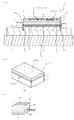
図1は、本発明に基づく光導波モジュール及びその実装構造の概略図である。
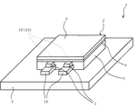
本実施の形態における光導波モジュールは、図2に示すように、前記光電変換素子としての光入射手段(例えば、半導体レーザー等の発光素子)3がシリコン等からなるサブマウント基板18に配置され、このサブマウント基板18を介して光入射手段3がインターポーザー5に配されている。なお、前記光電変換素子としての受光手段(例えば、フォトダイオード等の受光素子)4についても同様である。
図4に示すように、前記光入射手段としての前記発光素子としてECL(Extra Cavity Laser)21を用いてもよい。ECL21は、ハーフミラー22、レーザーを構成する増幅媒体23、MEMS(Micro Electro Mechanical Systems)可動ミラー24及び可動ミラー24に接合されたアクチュエータ25からなる。アクチュエータ25によって可動ミラー24の位置を動かすことによりレーザーのキャビティ長を変化させ、波長の異なるレーザー光(λ1、λ2)11を発生させることができる。これにより、光導波層10に複数の波長の光信号11を入射させることができ、例えばブロック毎に特定の波長のみを受光する受光素子4を設けることにより、LSI中の動作が必要なブロックだけにクロックを配信することができる。
前記光電変換素子としての前記受光手段は、例えばフォトダイオード等の受光素子が挙げられる。この受光手段は、例えば図5に示すように、実装基板6上に配置してもよい。具体的には、光導波層10の光出射端面17を傾斜面、例えば45度ミラー面に形成し、第1の半導体層7及びインターポーザー5における光出射端面17の直下に位置する領域に貫通孔26を設け、かつ実装基板6に凹部27を設け、この凹部27内に受光手段4を配置する。これにより、光導波層10の光出射端面17で導波光11が反射されて、受光手段4へ光路変換される。
5…インターポーザー、6…実装基板、7…第1の半導体層、8…絶縁層、
9…第2の半導体層、10…光導波層、11…光信号、12…集積回路、
13a、13b…クラッド層、14…活性層、15…電極、16…光入射端面、
17…光出射端面、18…サブマウント基板、19…アライメントマーク、
20…フォトディテクタ、21…ECL、22…ハーフミラー、23…増幅媒体、
24…可動ミラー、25…アクチュエータ、26…貫通孔、27…凹部
Claims (15)
- 第1の半導体層、絶縁層及び第2の半導体層とがこの順に積層され、前記第1の半導体層と前記第2の半導体層との間に光導波層が形成されている光導波装置と、光電変換素子とが、インターポーザーに配されている、光導波モジュール。
- 前記光電変換素子が、前記光導波装置の前記光導波層に光を入射させる光入射手段と、前記光導波層からの出射光を受光する受光手段とのうちの少なくとも前記光入射手段である、請求項1に記載した光導波モジュール。
- 前記光電変換素子がサブマウント基板に配置され、このサブマウント基板を介して前記光電変換素子が前記インターポーザーに配されている、請求項1に記載した光導波モジュール。
- 前記サブマウント基板上に、前記光電変換素子としての発光素子の出力をモニタできるフォトディテクタが配置されている、請求項3に記載した光導波モジュール。
- 前記第2の半導体層に集積回路が形成されている、請求項1に記載した光導波モジュール。
- 前記集積回路が、前記光電変換素子の駆動回路を有する、請求項5に記載した光導波モジュール。
- 前記光導波層の屈折率が、前記第1の半導体層及び前記絶縁層の屈折率より高い、請求項1に記載した光導波モジュール。
- 前記第1の半導体層としてのシリコン基体に不純物元素のドープによって前記光導波層が形成されている、請求項7に記載した光導波モジュール。
- 前記不純物元素がゲルマニウムからなる、請求項8に記載した光導波モジュール。
- 前記シリコン基体に前記光導波層としてのゲルマニウムドープのシリコン層が形成され、更にこのゲルマニウムドープのシリコン層上に、前記絶縁層としての酸化シリコン層及び前記第2の半導体層としてのシリコン層が設けられている、請求項9に記載した光導波モジュール。
- 前記サブマウント基板としてのシリコン基体に不純物元素のドープによって前記フォトディテクタが形成されている、請求項4に記載した光導波モジュール。
- 請求項1〜11のいずれか1項に記載した光導波モジュールが、前記インターポーザーを介して実装基板に実装されている、光導波モジュールの実装構造。
- 請求項2に記載した前記受光手段が前記インターポーザー上に配されている、請求項12に記載した光導波モジュールの実装構造。
- 請求項2に記載した前記受光手段が前記実装基板上に配されている、請求項12に記載した光導波モジュールの実装構造。
- 前記光導波層の光出射端面で導波光が反射されて、前記受光手段へ光路変換される、請求項14に記載した光導波モジュールの実装構造。
Priority Applications (1)
| Application Number | Priority Date | Filing Date | Title |
|---|---|---|---|
| JP2004236536A JP2006053473A (ja) | 2004-08-16 | 2004-08-16 | 光導波モジュール及びその実装構造 |
Applications Claiming Priority (1)
| Application Number | Priority Date | Filing Date | Title |
|---|---|---|---|
| JP2004236536A JP2006053473A (ja) | 2004-08-16 | 2004-08-16 | 光導波モジュール及びその実装構造 |
Publications (1)
| Publication Number | Publication Date |
|---|---|
| JP2006053473A true JP2006053473A (ja) | 2006-02-23 |
Family
ID=36030973
Family Applications (1)
| Application Number | Title | Priority Date | Filing Date |
|---|---|---|---|
| JP2004236536A Pending JP2006053473A (ja) | 2004-08-16 | 2004-08-16 | 光導波モジュール及びその実装構造 |
Country Status (1)
| Country | Link |
|---|---|
| JP (1) | JP2006053473A (ja) |
Cited By (4)
| Publication number | Priority date | Publication date | Assignee | Title |
|---|---|---|---|---|
| US8705906B2 (en) | 2009-04-23 | 2014-04-22 | Korea Electronics Technology Institute | Photoelectric conversion module |
| JP2018194648A (ja) * | 2017-05-16 | 2018-12-06 | 富士通オプティカルコンポーネンツ株式会社 | 光送信器及び光受信器 |
| JP2019207976A (ja) * | 2018-05-30 | 2019-12-05 | 日亜化学工業株式会社 | 光源装置 |
| CN117250702A (zh) * | 2023-11-20 | 2023-12-19 | 之江实验室 | 一种光电共封装模块及光电共封装方法 |
Citations (10)
| Publication number | Priority date | Publication date | Assignee | Title |
|---|---|---|---|---|
| JPS6188588A (ja) * | 1984-10-08 | 1986-05-06 | Sony Corp | 半導体レ−ザの製造方法 |
| JPS6190488A (ja) * | 1984-10-09 | 1986-05-08 | Sony Corp | 半導体装置とその製造方法 |
| JPS6195591A (ja) * | 1984-10-16 | 1986-05-14 | Sony Corp | 半導体レ−ザ |
| JPH11202159A (ja) * | 1998-01-19 | 1999-07-30 | Oki Electric Ind Co Ltd | 光回路モジュールの製造方法 |
| JP2000047055A (ja) * | 1998-07-28 | 2000-02-18 | Japan Aviation Electronics Industry Ltd | 光導波路デバイスおよびその製造方法 |
| JP2001183556A (ja) * | 1999-12-27 | 2001-07-06 | Toppan Printing Co Ltd | マルチチップモジュール基板及びマルチチップモジュール |
| JP2003222746A (ja) * | 2002-01-29 | 2003-08-08 | Mitsubishi Electric Corp | 光電気結合装置 |
| JP2003322741A (ja) * | 2002-05-08 | 2003-11-14 | Mitsubishi Electric Corp | 光電子混載基板 |
| EP1378777A2 (en) * | 2002-07-02 | 2004-01-07 | Omron Corporation | Optical waveguide device, manufacturing method thereof, and optical communication apparatus |
| WO2004010192A2 (en) * | 2002-07-22 | 2004-01-29 | Applied Materials Inc. | Optical-ready substrates with optical waveguide circuits and microelectronic circuits |
-
2004
- 2004-08-16 JP JP2004236536A patent/JP2006053473A/ja active Pending
Patent Citations (10)
| Publication number | Priority date | Publication date | Assignee | Title |
|---|---|---|---|---|
| JPS6188588A (ja) * | 1984-10-08 | 1986-05-06 | Sony Corp | 半導体レ−ザの製造方法 |
| JPS6190488A (ja) * | 1984-10-09 | 1986-05-08 | Sony Corp | 半導体装置とその製造方法 |
| JPS6195591A (ja) * | 1984-10-16 | 1986-05-14 | Sony Corp | 半導体レ−ザ |
| JPH11202159A (ja) * | 1998-01-19 | 1999-07-30 | Oki Electric Ind Co Ltd | 光回路モジュールの製造方法 |
| JP2000047055A (ja) * | 1998-07-28 | 2000-02-18 | Japan Aviation Electronics Industry Ltd | 光導波路デバイスおよびその製造方法 |
| JP2001183556A (ja) * | 1999-12-27 | 2001-07-06 | Toppan Printing Co Ltd | マルチチップモジュール基板及びマルチチップモジュール |
| JP2003222746A (ja) * | 2002-01-29 | 2003-08-08 | Mitsubishi Electric Corp | 光電気結合装置 |
| JP2003322741A (ja) * | 2002-05-08 | 2003-11-14 | Mitsubishi Electric Corp | 光電子混載基板 |
| EP1378777A2 (en) * | 2002-07-02 | 2004-01-07 | Omron Corporation | Optical waveguide device, manufacturing method thereof, and optical communication apparatus |
| WO2004010192A2 (en) * | 2002-07-22 | 2004-01-29 | Applied Materials Inc. | Optical-ready substrates with optical waveguide circuits and microelectronic circuits |
Cited By (6)
| Publication number | Priority date | Publication date | Assignee | Title |
|---|---|---|---|---|
| US8705906B2 (en) | 2009-04-23 | 2014-04-22 | Korea Electronics Technology Institute | Photoelectric conversion module |
| JP2018194648A (ja) * | 2017-05-16 | 2018-12-06 | 富士通オプティカルコンポーネンツ株式会社 | 光送信器及び光受信器 |
| JP2019207976A (ja) * | 2018-05-30 | 2019-12-05 | 日亜化学工業株式会社 | 光源装置 |
| JP7060798B2 (ja) | 2018-05-30 | 2022-04-27 | 日亜化学工業株式会社 | 光源装置 |
| CN117250702A (zh) * | 2023-11-20 | 2023-12-19 | 之江实验室 | 一种光电共封装模块及光电共封装方法 |
| CN117250702B (zh) * | 2023-11-20 | 2024-02-23 | 之江实验室 | 一种光电共封装模块及光电共封装方法 |
Similar Documents
| Publication | Publication Date | Title |
|---|---|---|
| CN114531920B (zh) | 使用微型发光二极管(microled)的芯片级光学互连 | |
| US10168474B2 (en) | Method of manufacturing optical input/output device | |
| CN108199779B (zh) | 用于通信的方法和系统 | |
| CN107040318B (zh) | 用于通信的方法和系统 | |
| US9331096B2 (en) | Method and system for hybrid integration of optical communication systems | |
| TWI522668B (zh) | Optical waveguide and optical waveguide module | |
| US9329349B2 (en) | Integrated optical cooling core for optoelectronic interconnect modules | |
| CN103580751B (zh) | 用于光通信系统的复合集成的方法和系统 | |
| JP2011028111A (ja) | 光i/oアレイモジュールおよびその製造方法 | |
| US20090297095A1 (en) | Planar optical waveguide array module and method of fabricating the same | |
| US20060120666A1 (en) | Optical waveguide device, manufacturing method thereof, optical information processing apparatus, and electronic equipment | |
| Schow et al. | A 24-channel, 300 Gb/s, 8.2 pJ/bit, full-duplex fiber-coupled optical transceiver module based on a single “Holey” CMOS IC | |
| US20120148190A1 (en) | Optical module and optical transmission device using the same | |
| JP4292476B2 (ja) | 光導波モジュール及び光情報処理装置 | |
| JP4412105B2 (ja) | 光導波装置 | |
| US10365431B2 (en) | Optical interconnect structure | |
| US20060024067A1 (en) | Optical I/O chip for use with distinct electronic chip | |
| JP2013012548A (ja) | 光モジュールおよび光電気混載ボード | |
| JP4654801B2 (ja) | 光電変換装置及びその製造方法、並びに光情報処理装置 | |
| JP5898732B2 (ja) | 光モジュールの製造方法 | |
| JP7688294B2 (ja) | 光モジュールおよびその作製方法 | |
| CN220568968U (zh) | 封装结构 | |
| JP2007019133A (ja) | 光電変換装置及びその製造方法、並びに光情報処理装置 | |
| JP2006053471A (ja) | 光導波装置及びその製造方法、並びに光情報処理装置 | |
| Liu et al. | Polymer waveguide applications in multichip modules (MCMs) and board level optical interconnects |
Legal Events
| Date | Code | Title | Description |
|---|---|---|---|
| RD13 | Notification of appointment of power of sub attorney |
Free format text: JAPANESE INTERMEDIATE CODE: A7433 Effective date: 20070125 |
|
| A621 | Written request for application examination |
Free format text: JAPANESE INTERMEDIATE CODE: A621 Effective date: 20070426 |
|
| A977 | Report on retrieval |
Free format text: JAPANESE INTERMEDIATE CODE: A971007 Effective date: 20090406 |
|
| A131 | Notification of reasons for refusal |
Free format text: JAPANESE INTERMEDIATE CODE: A131 Effective date: 20090414 |
|
| A521 | Request for written amendment filed |
Free format text: JAPANESE INTERMEDIATE CODE: A523 Effective date: 20090521 |
|
| RD02 | Notification of acceptance of power of attorney |
Free format text: JAPANESE INTERMEDIATE CODE: A7422 Effective date: 20090527 |
|
| A02 | Decision of refusal |
Free format text: JAPANESE INTERMEDIATE CODE: A02 Effective date: 20100323 |