JP2006067775A - DC / DC converter - Google Patents
DC / DC converter Download PDFInfo
- Publication number
- JP2006067775A JP2006067775A JP2005115249A JP2005115249A JP2006067775A JP 2006067775 A JP2006067775 A JP 2006067775A JP 2005115249 A JP2005115249 A JP 2005115249A JP 2005115249 A JP2005115249 A JP 2005115249A JP 2006067775 A JP2006067775 A JP 2006067775A
- Authority
- JP
- Japan
- Prior art keywords
- terminal
- transistor
- converter
- diode
- inductance
- Prior art date
- Legal status (The legal status is an assumption and is not a legal conclusion. Google has not performed a legal analysis and makes no representation as to the accuracy of the status listed.)
- Pending
Links
Images
Landscapes
- Dc-Dc Converters (AREA)
Abstract
【課題】
一般的に、これらのDC/DCコンバータは電源として用いられており、交流電源から変換された直流電源を入力するために用いられているものであり、夫々の機器の小型化から一層の簡素化と小型化が求められている。
【解決手段】
入力端子2に接続したトランジスタTr1と、トランジスタTr1に接続したインダクタンスL1と、インダクタンスL1に接続した出力端子3と、トランジスタTr1に接続した制御回路6と、トランジスタTr1とインダクタンスL1との間に接続したダイオードD1と、ダイオードD1に接続したグランド端子4とを備え、入力端子2とトランジスタTr1との間とグランド端子4とダイオードD1との間に第1のコンデンサC1を接続し、インダクタンスL1と出力端子との間とダイオードD1とグランド端子4との間に第2のコンデンサC2を接続した。
【選択図】
図1【Task】
Generally, these DC / DC converters are used as a power source, and are used for inputting a DC power source converted from an AC power source. Further simplification from the miniaturization of each device. And downsizing is required.
[Solution]
Transistor Tr1 connected to input terminal 2, inductance L1 connected to transistor Tr1, output terminal 3 connected to inductance L1, control circuit 6 connected to transistor Tr1, and connected between transistor Tr1 and inductance L1 A diode D1 and a ground terminal 4 connected to the diode D1 are provided. A first capacitor C1 is connected between the input terminal 2 and the transistor Tr1, and between the ground terminal 4 and the diode D1, and an inductance L1 and an output terminal. And a second capacitor C2 is connected between the diode D1 and the ground terminal 4.
[Selection]
FIG.
Description
本発明はDC/DCコンバータに関するものであり、更に詳細には、直流入力電圧を所定の直流出力電圧に変換すると共に、負荷側に何らかの原因により発生する過電流から保護をするための三端子型又は四端子形のDC/DCコンバータに関するものである。 The present invention relates to a DC / DC converter, and more specifically, a three-terminal type for converting a DC input voltage into a predetermined DC output voltage and protecting the load side from an overcurrent caused by some cause. Alternatively, the present invention relates to a four-terminal type DC / DC converter.
一般的に、これらのDC/DCコンバータはパーソナルコンピュータ、ゲーム機器、携帯機器等の電源として用いられており、商業用電源である交流電源から変換された直流電流を入力するために用いられているものであり、夫々の機器の小型化から一層の簡素化と小型化が求められているものである。 Generally, these DC / DC converters are used as power sources for personal computers, game machines, portable devices, and the like, and are used to input a DC current converted from an AC power source that is a commercial power source. There is a need for further simplification and miniaturization from the miniaturization of each device.
従来、例えば、誤差増幅回路15の出力端子とグランドGNDとの間にショート用トランジスタ31を接続し、ショート用トランジスタ31を初期誤動作防止回路12からLレベルの解除信号SG3が出力されるまで、即ち、三角波発振回路13が発振動作を開始されるまでオン状態にして誤差増幅回路15の誤差出力信号SG6が0ボルトに保持し、PWM比較回路17は、正常に発振動作を開始した三角波発振回路13の三角波信号SG3と、誤差増幅回路15が正常な状態で充電電圧Vsofと出力電圧Voutを比較しその差電圧を増幅して得た誤差出力信号SG6とに基づいてデューティ制御信号SG7を生成するもの(特許文献1参照)や、前記半導体スイッチング素子の出力端子と前記抵抗との接続点においてアノード端子を接続した第1のダイオード17と、前記第1のダイオードのカソード端子にベース端子を接続されエミッタ端子は前記半導体スイッチング素子のオン・オフ駆動用回路部のグランドに接続されたNPN型トランジスタ18と、前記NPN型トランジスタのコレクタ端子にベース端子を接続されコレクタ端子は前記NPN型トランジスタのベース端子に接続されたPNP型トランジスタ19と、前記半導体スイッチング素子のオン・オフ用入力端子にアノード端子を接続されカソード端子は前記NPN型トランジスタのコレクタ端子に接続された第2のダイオード20と、前記PNP型トランジスタのエミッタ端子に正極側を接続された第2の直流電源22とを備えたもの(特許文献2参照)等が開示されている。
然し乍ら、従来開示されているものは構成が複雑で、多数の制御回路やパーツを必要としており、その製造に多大の手間暇がかかり、高価なものと成っていた。 However, the conventionally disclosed one has a complicated structure and requires a large number of control circuits and parts, and it takes a lot of time and labor to manufacture the control circuit and parts.
前述の課題に鑑み、鋭意研鑽の結果、本発明のDC/DCコンバータは、コンバータ本体の一側面から入力端子と出力端子とグランド端子とを突出させた三端子型のDC/DCコンバータであって、入力端子に接続したトランジスタと、トランジスタに接続したインダクタンスと、インダクタンスに接続した出力端子と、トランジスタに接続した制御回路と、トランジスタとインダクタンスとの間の接続点に接続したダイオードと、ダイオードに接続したグランド端子とを備え、入力端子とトランジスタとの間とグランド端子とダイオードとの間に夫々接続点を設けて第1のコンデンサを接続し、インダクタンスと出力端子との間とダイオードとグランド端子との間に夫々接続点を設けて第2のコンデンサを接続したものであり、又は、コンバータ本体の一側面から入力端子と出力端子とグランド端子と出力電圧可変端子とを突出させた四端子型のDC/DCコンバータであって、入力端子に接続したトランジスタと、トランジスタに接続したインダクタンスと、インダクタンスに接続した出力端子と、トランジスタに接続した制御回路と、トランジスタとインダクタンスとの間の接続点に接続したダイオードと、ダイオードに接続したグランド端子とを備え、入力端子とトランジスタとの間とグランド端子とダイオードとの間に夫々接続点を設けて第1のコンデンサを接続し、インダクタンスと出力端子との間とダイオードとグランド端子との間に夫々接続点を設けて第2のコンデンサを接続すると共に、制御回路と出力電圧可変端子を接続し、出力電圧可変端子と出力端子との間に第1の任意抵抗を接続し、出力電圧可変端子とグランド端子との間に第2の任意抵抗を接続したものである。 As a result of diligent research, the DC / DC converter of the present invention is a three-terminal DC / DC converter in which an input terminal, an output terminal, and a ground terminal are projected from one side of the converter body. A transistor connected to the input terminal, an inductance connected to the transistor, an output terminal connected to the inductance, a control circuit connected to the transistor, a diode connected to a connection point between the transistor and the inductance, and a connection to the diode A ground capacitor, a connection point is provided between the input terminal and the transistor, and between the ground terminal and the diode to connect the first capacitor, and between the inductance and the output terminal, between the diode and the ground terminal, A connection point is provided between the two capacitors and a second capacitor is connected. A four-terminal type DC / DC converter in which an input terminal, an output terminal, a ground terminal, and an output voltage variable terminal are projected from one side of the data body, a transistor connected to the input terminal, and an inductance connected to the transistor An output terminal connected to the inductance, a control circuit connected to the transistor, a diode connected to a connection point between the transistor and the inductance, and a ground terminal connected to the diode, between the input terminal and the transistor And connecting a first capacitor between the ground terminal and the diode, and connecting a first capacitor between the inductance and the output terminal and between the diode and the ground terminal. Connect the control circuit and the output voltage variable terminal, and connect the output voltage variable terminal and the output terminal. First connecting any resistance, it is obtained by connecting the second optional resistor between the output voltage variable terminal and ground terminal.
本発明の三端子型のDC/DCコンバータは、入力端子とトランジスタのコレクタ端子との間とグランド端子とダイオードのアノード端子との間に夫々接続点を設けて第1のコンデンサを接続し、インダクタンスと出力端子との間とダイオードのアノード端子とグランド端子との間に夫々接続点を設けて第2のコンデンサを接続し、更に、四端子型のDC/DCコンバータは、入力端子とトランジスタのコレクタ端子との間とグランド端子とダイオードのアノード端子との間に夫々接続点を設けて第1のコンデンサを接続し、インダクタンスと出力端子との間とダイオードのアノード端子とグランド端子との間に夫々接続点を設けて第2のコンデンサを接続すると共に、制御回路に出力電圧可変端子を接続し、出力電圧可変端子と出力端子との間に第1の任意抵抗をグランド端子との間に第2の任意抵抗を接続したたことにより、構成を簡素化できパーツの組み込みが少ないため、廉価で提供できるものであり、画期的で実用性の高い発明である。 The three-terminal type DC / DC converter according to the present invention has a connection point between the input terminal and the collector terminal of the transistor, and between the ground terminal and the anode terminal of the diode, and connects the first capacitor to the inductance. And the output terminal, and between the anode terminal of the diode and the ground terminal, respectively, are connected to the second capacitor, and the four-terminal DC / DC converter includes an input terminal and a collector of a transistor. The first capacitor is connected by providing connection points between the terminals, between the ground terminal and the anode terminal of the diode, and between the inductance and the output terminal, and between the anode terminal and the ground terminal of the diode. A connection point is provided to connect the second capacitor, and the output voltage variable terminal is connected to the control circuit. The output voltage variable terminal and the output terminal Since the first arbitrary resistor is connected between the second arbitrary resistor and the ground terminal, the configuration can be simplified and the number of parts incorporated is small, so it can be provided at a low price, and is innovative. It is a highly practical invention.
本発明はDC/DCコンバータに関するものであり、更に詳細には、直流入力電圧を所定の直流出力電圧に変換すると共に、負荷側に何らかの原因により発生する過電流から保護をする三端子型又は四端子型のDC/DCコンバータに関するものであり、請求項1に記載のDC/DCコンバータは、コンバータ本体1の一側面から入力端子2と出力端子3とグランド端子4とを突出させた三端子型のDC/DCコンバータであって、前記入力端子2にコレクタ端子を接続したトランジスタTr1と、該トランジスタTr1のエミッタ端子に接続したインダクタンスL1と、該インダクタンスL1に接続した出力端子3と、前記トランジスタTr1のベース端子に接続した制御回路6と、前記トランジスタTr1のエミッタ端子とインダクタンスL1との間の接続点にカソード端子を接続したダイオードD1と、該ダイオードD1のアノード端子に接続したグランド端子4とを備え、前記入力端子2とトランジスタTr1のコレクタ端子との間とグランド端子4とダイオードD1のアノード端子との間に夫々接続点を設けて第1のコンデンサC1を接続し、前記インダクタンスL1と出力端子との間とダイオードD1のアノード端子とグランド端子4との間に夫々接続点を設けて第2のコンデンサC2を接続したものである。
The present invention relates to a DC / DC converter. More specifically, the present invention converts a DC input voltage into a predetermined DC output voltage, and protects against an overcurrent generated for some reason on the load side. The DC / DC converter according to
更に、請求項2に記載のDC/DCコンバータは、コンバータ本体1の一側面から入力端子2と出力端子3とグランド端子4と出力電圧可変端子5とを突出させた四端子型のDC/DCコンバータであって、前記入力端子2にコレクタ端子を接続したトランジスタTr1と、該トランジスタTr1のエミッタ端子に接続したインダクタンスL1と、該インダクタンスL1に接続した出力端子3と、前記トランジスタTr1のベース端子に接続した制御回路6と、前記トランジスタTr1のエミッタ端子とインダクタンスL1との間の接続点にカソード端子を接続したダイオードD1と、該ダイオードD1のアノード端子に接続したグランド端子4とを備え、前記入力端子2とトランジスタTr1のコレクタ端子との間とグランド端子4とダイオードD1のアノード端子との間に夫々接続点を設けて第1のコンデンサC1を接続し、前記インダクタンスL1と出力端子との間とダイオードD1のアノード端子とグランド端子4との間に夫々接続点を設けて第2のコンデンサC2を接続すると共に、前記制御回路6と出力電圧可変端子5を接続し、該出力電圧可変端子5と出力端子3との間に第1の任意抵抗VR1を接続し、前記出力電圧可変端子5とグランド端子4との間に第2の任意抵抗VR2を接続したたものである。
The DC / DC converter according to
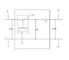
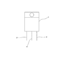
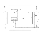
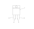
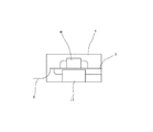
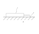
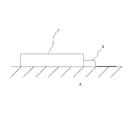
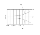
以下、本発明のDC/DCコンバータの実施例の図面を用いて詳細に説明すると、図1は本発明のDC/DCコンバータの実施例の三端子型のDC/DCコンバータの回路図であり、図2は本発明のDC/DCコンバータの実施例の三端子型のDC/DCコンバータの正面図であり、図3は本発明のDC/DCコンバータの次実施例の四端子型のDC/DCコンバータの回路図であり、図4はDC/DCコンバータの次実施例の四端子型のDC/DCコンバータの正面図であり、図5は本発明のDC/DCコンバータの内部を説明するための断面説明図であり、図6は本発明のDC/DCコンバータの実装状態を説明するための側面図であり、図7は本発明のDC/DCコンバータの他の実装状態を説明するための側面図であり、図8は本発明のDC/DCコンバータの次実施例の四端子型のDC/DCコンバータの任意抵抗の出力電圧と抵抗値を表したグラフである。 Hereinafter, a DC / DC converter according to an embodiment of the present invention will be described in detail with reference to the drawings. FIG. 1 is a circuit diagram of a three-terminal DC / DC converter according to an embodiment of the DC / DC converter of the present invention. FIG. 2 is a front view of a three-terminal DC / DC converter according to an embodiment of the DC / DC converter of the present invention, and FIG. 3 is a four-terminal DC / DC according to the next embodiment of the DC / DC converter according to the present invention. FIG. 4 is a circuit diagram of the converter, FIG. 4 is a front view of a four-terminal type DC / DC converter of the next embodiment of the DC / DC converter, and FIG. 5 is for explaining the inside of the DC / DC converter of the present invention. FIG. 6 is a cross-sectional explanatory view, FIG. 6 is a side view for explaining a mounted state of the DC / DC converter of the present invention, and FIG. 7 is a side view for explaining another mounted state of the DC / DC converter of the present invention. Fig. 8 shows The following examples of the DC / DC converter is a graph showing the output voltage and the resistance value of any resistor of the four-terminal type DC / DC converter.
即ち、本発明の実施例の三端子型のDC/DCコンバータは、図2に図示する如く、コンバータ本体1は絶縁部材で形成された略立方体状のもので、一側面には機器と電気的に接続させるための入力端子2と出力端子3とグランド端子4とを突出させているものである。
That is, in the three-terminal type DC / DC converter of the embodiment of the present invention, as shown in FIG. 2, the converter
そして、図1に図示する実施例の回路図の如く、トランジスタTr1
はコレクタ端子を入力端子に接続し、エミッタ端子は後述するダイオードD1のカソード端子との接続点を介装してインダクタンスL1と接続し、ベース端子には後述する制御回路6と接続しているものである。
As shown in the circuit diagram of the embodiment shown in FIG.
Has a collector terminal connected to an input terminal, an emitter terminal connected to an inductance L1 via a connection point with a cathode terminal of a diode D1 described later, and a base terminal connected to a control circuit 6 described later. It is.
次に、制御回路6はトランジスタTr1のベース端子に接続させているものである。 Next, the control circuit 6 is connected to the base terminal of the transistor Tr1.
次いで、インダクタンスL1は一方をトランジスタTr1のエミッタ端子と後述するダイオードD1のカソード端子との接続点を介装して接続すると共に、インダクタンスL1の他方は出力端子と後述する第2のコンデンサC2を接続するための接続点を介装して接続しているものである。 Next, one side of the inductance L1 is connected via a connection point between the emitter terminal of the transistor Tr1 and the cathode terminal of the diode D1 described later, and the other side of the inductance L1 connects the output terminal and the second capacitor C2 described later. It is connected via a connection point for the purpose.
更に、ダイオードD1はカソード端子をトランジスタTr1のエミッタ端子とインダクタンスL1との間の接続点に接続すると共に、ダイオードD1のアノード端子はグランド端子4に接続しているものである。
Further, the diode D1 has a cathode terminal connected to a connection point between the emitter terminal of the transistor Tr1 and the inductance L1, and an anode terminal of the diode D1 is connected to the
そして、第1のコンデンサC1は入力端子2とトランジスタTr1のコレクタ端子との間に接続点を設けると共に、グランド端子4とダイオードD1のアノード端子との間に接続点を設け、夫々の接続点との間に配設したものである。
The first capacitor C1 has a connection point between the
次いで、第2のコンデンサC2はインダクタンスL1と出力端子3との間に接続点を設けると共に、ダイオードD1のアノード端子とグランド端子4との間に接続点を設け、夫々の接続点との間に配設したものである。
Next, the second capacitor C2 is provided with a connection point between the inductance L1 and the
更には、本発明の三端子型のDC/DCコンバータの実装状態は図5に図示する如く、コンバータ本体1の一側面に入力端子2と出力端子3とグランド端子4とを突出させ、略中央に上下に仕切るように絶縁体7を内装し、絶縁体7の上方に回路を形成した半導体チップ8を取り付けると共に、絶縁体7の下方に誘電体であるインダクタンスL1を取り付けたものである。
Furthermore, the mounting state of the three-terminal type DC / DC converter of the present invention is as shown in FIG. 5, in which an
そして、本発明の次実施例の四端子型のDC/DCコンバータは、図3及び図4に図示する如く、前述の三端子型のDC/DCコンバータに出力電圧可変端子5を付設したもので、出力電圧可変端子5は制御回路6と接続をしており、コンバータ本体1の一側面に入力端子2と出力端子3とグランド端子4と並設して突設しているものであり、加えて、前記出力電圧可変端子5と出力端子3との間に電圧を上げるための第1の任意抵抗VR1を接続し、前記出力電圧可変端子5とグランド端子4との間に電圧を下げるための第2の任意抵抗VR2を接続したものである。
The four-terminal type DC / DC converter of the next embodiment of the present invention is obtained by adding the output
更には、第1の任意抵抗VR1と第2の任意抵抗VR2とは、例えば、図8に図示するグラフのように使用する出力電圧によって任意に設定して接続するものであり、他の構造は実施例の三端子型のDC/DCコンバータと同様であるので省略するものである。 Furthermore, the first arbitrary resistor VR1 and the second arbitrary resistor VR2 are connected by being arbitrarily set according to the output voltage used as shown in the graph shown in FIG. 8, for example. Since it is similar to the three-terminal type DC / DC converter of the embodiment, it is omitted.
更に、本発明のDC/DCコンバータを基板Aの上に実装するには、図6に図示する如く、基板Aに設けた孔に三端子2.3.4又は四端子2.3.4.5の先端を挿通させて半田で取り付けを行うディスクリートタイプでも、或いは、基板Aに三端子2.3.4又は四端子2.3.4.5の先端辺を半田のリフローを利用して取り付けを行う表面実装タイプで可能なものである。 Further, in order to mount the DC / DC converter of the present invention on the board A, as shown in FIG. 6, the three terminals 2.3.4 or the four terminals 2.3.4. Discrete type with 5 tip inserted and soldered, or 3 terminal 2.3.4 or 4 terminal 2.3.4.5 attached to substrate A using solder reflow This is possible with the surface mount type.
本発明の三端子型又は四端子型のDC/DCコンバータは、携帯機器等に用いるもので、5〜40Vの直流入力電圧を1.5〜30Vの直流出力電圧にコンバートするものであり、保護回路として過電流保護、過熱保護に最適のものである。 The three-terminal type or four-terminal type DC / DC converter of the present invention is used for portable devices and the like, and converts a DC input voltage of 5 to 40 V into a DC output voltage of 1.5 to 30 V, and is protected. The circuit is ideal for overcurrent protection and overheat protection.
1 コンバータ本体
2 入力端子
3 出力端子
4 グランド端子
5 出力電圧可変端子
6 制御回路
7 絶縁体
8 半導体チップ
Tr1 トランジスタ
L1 インダクタンス
D1 ダイオード
C1 第1のコンデンサ
C2 第2のコンデンサ
VR1 第1の任意抵抗
VR2 第2の任意抵抗
A 基板
DESCRIPTION OF
Claims (2)
A four-terminal type DC / DC converter in which an input terminal, an output terminal, a ground terminal, and an output voltage variable terminal protrude from one side of a converter body, the transistor having a collector terminal connected to the input terminal, and the transistor An inductance connected to the emitter terminal of the transistor, an output terminal connected to the inductance, a control circuit connected to the base terminal of the transistor, and a diode having a cathode terminal connected to a connection point between the emitter terminal and the inductance of the transistor And a ground terminal connected to the anode terminal of the diode, and a first capacitor is provided by providing connection points between the input terminal and the collector terminal of the transistor and between the ground terminal and the anode terminal of the diode, respectively. Connect and diode between the inductance and the output terminal A connection point is provided between the anode terminal and the ground terminal to connect the second capacitor, and the control circuit and the output voltage variable terminal are connected, and the first voltage is provided between the output voltage variable terminal and the output terminal. The DC / DC converter is characterized in that a second arbitrary resistor is connected between the output voltage variable terminal and the ground terminal.
Priority Applications (1)
| Application Number | Priority Date | Filing Date | Title |
|---|---|---|---|
| JP2005115249A JP2006067775A (en) | 2004-07-26 | 2005-04-13 | DC / DC converter |
Applications Claiming Priority (2)
| Application Number | Priority Date | Filing Date | Title |
|---|---|---|---|
| JP2004216724 | 2004-07-26 | ||
| JP2005115249A JP2006067775A (en) | 2004-07-26 | 2005-04-13 | DC / DC converter |
Publications (2)
| Publication Number | Publication Date |
|---|---|
| JP2006067775A true JP2006067775A (en) | 2006-03-09 |
| JP2006067775A5 JP2006067775A5 (en) | 2007-05-31 |
Family
ID=36113738
Family Applications (1)
| Application Number | Title | Priority Date | Filing Date |
|---|---|---|---|
| JP2005115249A Pending JP2006067775A (en) | 2004-07-26 | 2005-04-13 | DC / DC converter |
Country Status (1)
| Country | Link |
|---|---|
| JP (1) | JP2006067775A (en) |
Cited By (1)
| Publication number | Priority date | Publication date | Assignee | Title |
|---|---|---|---|---|
| JP2013534398A (en) * | 2010-07-27 | 2013-09-02 | イヴァン ジャマエブ,ジャック | Method and apparatus for dimming illumination with sinusoidal waves in phase |
-
2005
- 2005-04-13 JP JP2005115249A patent/JP2006067775A/en active Pending
Cited By (1)
| Publication number | Priority date | Publication date | Assignee | Title |
|---|---|---|---|---|
| JP2013534398A (en) * | 2010-07-27 | 2013-09-02 | イヴァン ジャマエブ,ジャック | Method and apparatus for dimming illumination with sinusoidal waves in phase |
Similar Documents
| Publication | Publication Date | Title |
|---|---|---|
| US10367419B2 (en) | Power conversion device with integrated discrete inductor | |
| JP4995890B2 (en) | Semiconductor device and DC-DC converter | |
| US12567802B2 (en) | Voltage convertor module including a lead-frame, a unitary bare die and a molding body | |
| JP2006271048A (en) | Motor drive device | |
| JP4808979B2 (en) | Multi-chip type semiconductor device and manufacturing method thereof | |
| US7403399B2 (en) | Active primary-sided circuit arrangement for a switch-mode power supply | |
| US6625031B2 (en) | Module part and electronic device | |
| JP2006067775A (en) | DC / DC converter | |
| JP3165911U (en) | DC / DC converter | |
| JP2008251901A (en) | Composite semiconductor device | |
| US20070091659A1 (en) | Power converter comprising a controller and a power component mounted on separate circuit boards | |
| JP4957183B2 (en) | Semiconductor device using backside high voltage integrated circuit | |
| JP4367774B2 (en) | IC chip | |
| JP3620766B2 (en) | Voltage supply circuit for amplifier | |
| US7304465B2 (en) | Power supply circuit capable of efficiently supplying a supply voltage | |
| JP2006166142A (en) | Overcurrent protection circuit and inverter provided with the same | |
| JP3425961B2 (en) | Control circuit device | |
| JP2006054245A (en) | Semiconductor device | |
| JP2006014491A (en) | Power input circuit | |
| JPS63257420A (en) | Inrush current prevention circuit | |
| JP2580798B2 (en) | Transistor module for power converter | |
| JP2011199985A (en) | Dc-dc converter | |
| JP2009245999A (en) | Semiconductor device, and semiconductor integrated device | |
| JP2006345618A (en) | Motor drive device | |
| JP3494601B2 (en) | Power supply |
Legal Events
| Date | Code | Title | Description |
|---|---|---|---|
| A521 | Written amendment |
Free format text: JAPANESE INTERMEDIATE CODE: A523 Effective date: 20070410 |
|
| A621 | Written request for application examination |
Effective date: 20070410 Free format text: JAPANESE INTERMEDIATE CODE: A621 |
|
| RD02 | Notification of acceptance of power of attorney |
Effective date: 20070410 Free format text: JAPANESE INTERMEDIATE CODE: A7422 |
|
| A977 | Report on retrieval |
Free format text: JAPANESE INTERMEDIATE CODE: A971007 Effective date: 20091111 |
|
| A131 | Notification of reasons for refusal |
Effective date: 20091124 Free format text: JAPANESE INTERMEDIATE CODE: A131 |
|
| A521 | Written amendment |
Free format text: JAPANESE INTERMEDIATE CODE: A523 Effective date: 20100125 |
|
| A02 | Decision of refusal |
Effective date: 20100302 Free format text: JAPANESE INTERMEDIATE CODE: A02 |