JP2006100600A - 半導体装置およびその製造方法 - Google Patents
半導体装置およびその製造方法 Download PDFInfo
- Publication number
- JP2006100600A JP2006100600A JP2004285462A JP2004285462A JP2006100600A JP 2006100600 A JP2006100600 A JP 2006100600A JP 2004285462 A JP2004285462 A JP 2004285462A JP 2004285462 A JP2004285462 A JP 2004285462A JP 2006100600 A JP2006100600 A JP 2006100600A
- Authority
- JP
- Japan
- Prior art keywords
- semiconductor
- metal
- mos transistor
- channel
- regions
- Prior art date
- Legal status (The legal status is an assumption and is not a legal conclusion. Google has not performed a legal analysis and makes no representation as to the accuracy of the status listed.)
- Abandoned
Links
Images














Classifications
-
- H—ELECTRICITY
- H10—SEMICONDUCTOR DEVICES; ELECTRIC SOLID-STATE DEVICES NOT OTHERWISE PROVIDED FOR
- H10D—INORGANIC ELECTRIC SEMICONDUCTOR DEVICES
- H10D30/00—Field-effect transistors [FET]
- H10D30/60—Insulated-gate field-effect transistors [IGFET]
- H10D30/62—Fin field-effect transistors [FinFET]
-
- H—ELECTRICITY
- H10—SEMICONDUCTOR DEVICES; ELECTRIC SOLID-STATE DEVICES NOT OTHERWISE PROVIDED FOR
- H10D—INORGANIC ELECTRIC SEMICONDUCTOR DEVICES
- H10D30/00—Field-effect transistors [FET]
- H10D30/01—Manufacture or treatment
- H10D30/021—Manufacture or treatment of FETs having insulated gates [IGFET]
- H10D30/024—Manufacture or treatment of FETs having insulated gates [IGFET] of fin field-effect transistors [FinFET]
-
- H—ELECTRICITY
- H10—SEMICONDUCTOR DEVICES; ELECTRIC SOLID-STATE DEVICES NOT OTHERWISE PROVIDED FOR
- H10D—INORGANIC ELECTRIC SEMICONDUCTOR DEVICES
- H10D30/00—Field-effect transistors [FET]
- H10D30/01—Manufacture or treatment
- H10D30/021—Manufacture or treatment of FETs having insulated gates [IGFET]
- H10D30/027—Manufacture or treatment of FETs having insulated gates [IGFET] of lateral single-gate IGFETs
- H10D30/0277—Manufacture or treatment of FETs having insulated gates [IGFET] of lateral single-gate IGFETs forming conductor-insulator-semiconductor or Schottky barrier source or drain regions
-
- H—ELECTRICITY
- H10—SEMICONDUCTOR DEVICES; ELECTRIC SOLID-STATE DEVICES NOT OTHERWISE PROVIDED FOR
- H10D—INORGANIC ELECTRIC SEMICONDUCTOR DEVICES
- H10D30/00—Field-effect transistors [FET]
- H10D30/60—Insulated-gate field-effect transistors [IGFET]
- H10D30/67—Thin-film transistors [TFT]
- H10D30/6729—Thin-film transistors [TFT] characterised by the electrodes
- H10D30/673—Thin-film transistors [TFT] characterised by the electrodes characterised by the shapes, relative sizes or dispositions of the gate electrodes
- H10D30/6735—Thin-film transistors [TFT] characterised by the electrodes characterised by the shapes, relative sizes or dispositions of the gate electrodes having gates fully surrounding the channels, e.g. gate-all-around
-
- H—ELECTRICITY
- H10—SEMICONDUCTOR DEVICES; ELECTRIC SOLID-STATE DEVICES NOT OTHERWISE PROVIDED FOR
- H10D—INORGANIC ELECTRIC SEMICONDUCTOR DEVICES
- H10D30/00—Field-effect transistors [FET]
- H10D30/01—Manufacture or treatment
- H10D30/021—Manufacture or treatment of FETs having insulated gates [IGFET]
- H10D30/027—Manufacture or treatment of FETs having insulated gates [IGFET] of lateral single-gate IGFETs
- H10D30/0275—Manufacture or treatment of FETs having insulated gates [IGFET] of lateral single-gate IGFETs forming single crystalline semiconductor source or drain regions resulting in recessed gates, e.g. forming raised source or drain regions
-
- H—ELECTRICITY
- H10—SEMICONDUCTOR DEVICES; ELECTRIC SOLID-STATE DEVICES NOT OTHERWISE PROVIDED FOR
- H10D—INORGANIC ELECTRIC SEMICONDUCTOR DEVICES
- H10D30/00—Field-effect transistors [FET]
- H10D30/60—Insulated-gate field-effect transistors [IGFET]
- H10D30/62—Fin field-effect transistors [FinFET]
- H10D30/6218—Fin field-effect transistors [FinFET] of the accumulation type
-
- H—ELECTRICITY
- H10—SEMICONDUCTOR DEVICES; ELECTRIC SOLID-STATE DEVICES NOT OTHERWISE PROVIDED FOR
- H10D—INORGANIC ELECTRIC SEMICONDUCTOR DEVICES
- H10D30/00—Field-effect transistors [FET]
- H10D30/60—Insulated-gate field-effect transistors [IGFET]
- H10D30/67—Thin-film transistors [TFT]
- H10D30/6704—Thin-film transistors [TFT] having supplementary regions or layers in the thin films or in the insulated bulk substrates for controlling properties of the device
- H10D30/6713—Thin-film transistors [TFT] having supplementary regions or layers in the thin films or in the insulated bulk substrates for controlling properties of the device characterised by the properties of the source or drain regions, e.g. compositions or sectional shapes
Landscapes
- Electrodes Of Semiconductors (AREA)
- Thin Film Transistor (AREA)
Abstract
【解決手段】 チャネル型が第1導電型であるMOSトランジスタは、第1および第2のチャネル領域CHを含む第1導電型半導体領域1と、第1および第2のチャネル領域CH上に設けられたゲート絶縁膜2と、ゲート絶縁膜2上に設けられたゲート電極3と、第1および第2のチャネル領域CHを挟むように設けられ、かつ、第1導電型半導体領域1とショットキー接合する、互いに離間した第1および第2のソース/ドレイン領域4を備えている。
【選択図】 図1
Description
Jakub Kedzierski et al., IEDM Technical digest, pp. 57-60, (2000)
図1は、本発明の第1の実施形態に係るSchottky−S/D構造を含むMOSトランジスタの模式図である。本実施形態のMOSトランジスタは例えばLogic−LSIに使用されるものである。
図2は、本発明の第2の実施形態に係るSchottky−S/D構造を含むMOSトランジスタの模式図である。なお、図2において、図1と対応する部分には図1と同一符号を付してあり、詳細な説明は省略する。
図3−図15は、本発明の第3の実施形態に係るSchottky−S/D構造を含むMOSトランジスタの製造プロセスを示す断面図である。本実施形態のMOSトランジスタは例えばLogic−LSIに使用されるものである。本実施形態のMOSトランジスタは、第1の実施形態のMOSトランジスタの具体例に相当する。
図17−図23は、本発明の第4の実施形態に係るSchottky−S/D構造を含むMOSトランジスタの製造プロセスを示す断面図である。本実施形態のMOSトランジスタは例えばLogic−LSIに使用されるものである。本実施形態のMOSトランジスタは、第2の実施形態のMOSトランジスタの具体例に相当する。
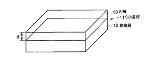
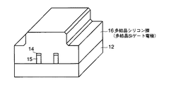
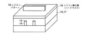
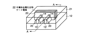
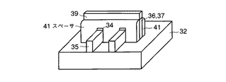
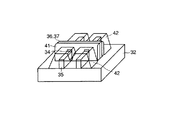
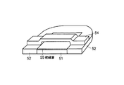
図25−図27は、本発明の第5の実施形態に係るSchottky−S/D構造を含むMOSトランジスタの製造プロセスを示す斜視図である。本実施形態のMOSトランジスタは例えばLogic−LSIに使用されるものである。
Claims (5)
- 半導体基板と、
前記半導体基板上に設けられ、チャネル型が第1導電型であるMOSトランジスタであって、第1および第2のチャネル領域を含む第1導電型半導体領域と、前記第1および第2のチャネル領域上に設けられたゲート絶縁膜と、前記ゲート絶縁膜上に設けられたゲート電極と、前記第1および第2のチャネル領域を挟むように設けられ、かつ、前記第1導電型半導体領域とショットキー接合する、互いに離間した第1および第2のソース/ドレイン領域とを備えた前記MOSトランジスタと
を具備してなることを特徴とする半導体装置。 - 前記ゲート電極は第1の金属半導体化合物または金属を含み、前記第1および第2のソース/ドレイン領域は第2の金属半導体化合物または金属を含むことを特徴とする請求項1に記載の半導体装置。
- 前記第1の金属半導体化合物と前記第2の金属半導体化合物は、同じ材料であることを特徴とする請求項2に記載の半導体装置。
- 半導体基板上にチャネル型が第1導電型であるMOSトランジスタを形成する工程とを含む半導体装置の製造方法であって、
前記MOSトランジスタを形成する工程は、
第1および第2のソース/ドレイン領域となる第1および第2の半導体領域、ならびに、第1および第2のチャネル領域を含む、第1導電型半導体領域を形成する工程と、
前記第1および第2のチャネル領域上にゲート絶縁膜を介して半導体膜を形成する工程と、
前記第1および第2の半導体領域ならびに前記半導体膜を、金属と半導体を含む金属半導体化合物領域に変える工程と
を有することを特徴とする半導体装置の製造方法。 - 半導体基板上にチャネル型が第1導電型であるMOSトランジスタを形成する工程とを含む半導体装置の製造方法であって、
前記MOSトランジスタを形成する工程は、
第1および第2のソース/ドレイン領域となる第1および第2の半導体領域、ならびに、第1および第2のチャネル領域を含む、第1導電型半導体領域を形成する工程と、
前記第1および第2のチャネル領域上にゲート絶縁膜を介して半導体膜を形成する工程と、
前記第1および第2の半導体領域ならびに前記半導体膜を除去した領域上に、金属材料を堆積する工程と
を有することを特徴とする半導体装置の製造方法。
Priority Applications (2)
| Application Number | Priority Date | Filing Date | Title |
|---|---|---|---|
| JP2004285462A JP2006100600A (ja) | 2004-09-29 | 2004-09-29 | 半導体装置およびその製造方法 |
| US11/236,723 US7405449B2 (en) | 2004-09-29 | 2005-09-28 | Semiconductor device and method of manufacturing the same |
Applications Claiming Priority (1)
| Application Number | Priority Date | Filing Date | Title |
|---|---|---|---|
| JP2004285462A JP2006100600A (ja) | 2004-09-29 | 2004-09-29 | 半導体装置およびその製造方法 |
Publications (1)
| Publication Number | Publication Date |
|---|---|
| JP2006100600A true JP2006100600A (ja) | 2006-04-13 |
Family
ID=36124700
Family Applications (1)
| Application Number | Title | Priority Date | Filing Date |
|---|---|---|---|
| JP2004285462A Abandoned JP2006100600A (ja) | 2004-09-29 | 2004-09-29 | 半導体装置およびその製造方法 |
Country Status (2)
| Country | Link |
|---|---|
| US (1) | US7405449B2 (ja) |
| JP (1) | JP2006100600A (ja) |
Cited By (5)
| Publication number | Priority date | Publication date | Assignee | Title |
|---|---|---|---|---|
| US7683437B2 (en) | 2006-08-30 | 2010-03-23 | Elpida Memory, Inc. | Semiconductor device having fin field effect transistor and manufacturing method thereof |
| US7902584B2 (en) | 2007-04-16 | 2011-03-08 | Kabushiki Kaisha Toshiba | Semiconductor memory device and manufacturing method thereof |
| US8574993B2 (en) | 2009-09-16 | 2013-11-05 | Kabushiki Kaisha Toshiba | Semiconductor device and method of manufacturing the same |
| JP2021196046A (ja) * | 2020-06-18 | 2021-12-27 | 株式会社オリジン | トルクリミッタ |
| US11646380B2 (en) | 2013-05-20 | 2023-05-09 | Semiconductor Energy Laboratory Co., Ltd. | Semiconductor device |
Families Citing this family (15)
| Publication number | Priority date | Publication date | Assignee | Title |
|---|---|---|---|---|
| KR100578818B1 (ko) * | 2005-02-24 | 2006-05-11 | 삼성전자주식회사 | 핀 전계 효과 트랜지스터 및 이의 형성 방법 |
| US20060251872A1 (en) * | 2005-05-05 | 2006-11-09 | Wang Jenn Y | Conductive barrier layer, especially an alloy of ruthenium and tantalum and sputter deposition thereof |
| US20070059502A1 (en) * | 2005-05-05 | 2007-03-15 | Applied Materials, Inc. | Integrated process for sputter deposition of a conductive barrier layer, especially an alloy of ruthenium and tantalum, underlying copper or copper alloy seed layer |
| US8138527B2 (en) * | 2006-07-13 | 2012-03-20 | National University Corporation Tohoku University | Transistor and semiconductor device |
| US8362567B2 (en) * | 2006-07-13 | 2013-01-29 | National University Corporation Tohoku University | Semiconductor device |
| US7858471B2 (en) * | 2006-09-13 | 2010-12-28 | Micron Technology, Inc. | Methods of fabricating an access transistor for an integrated circuit device, methods of fabricating periphery transistors and access transistors, and methods of fabricating an access device comprising access transistors in an access circuitry region and peripheral transistors in a peripheral circuitry region spaced from the access circuitry region |
| US7692254B2 (en) * | 2007-07-16 | 2010-04-06 | International Business Machines Corporation | Fin-type field effect transistor structure with merged source/drain silicide and method of forming the structure |
| JP5769160B2 (ja) * | 2008-10-30 | 2015-08-26 | 国立大学法人東北大学 | コンタクト形成方法、半導体装置の製造方法、および半導体装置 |
| US9054194B2 (en) | 2009-04-29 | 2015-06-09 | Taiwan Semiconductor Manufactruing Company, Ltd. | Non-planar transistors and methods of fabrication thereof |
| CN101930915B (zh) * | 2009-06-26 | 2012-05-23 | 中国科学院微电子研究所 | 一种钼铝氮金属栅的制备方法 |
| TWI671910B (zh) | 2012-09-24 | 2019-09-11 | 日商半導體能源研究所股份有限公司 | 半導體裝置 |
| US9397217B2 (en) * | 2012-12-28 | 2016-07-19 | Taiwan Semiconductor Manufacturing Company, Ltd. | Contact structure of non-planar semiconductor device |
| US9590105B2 (en) * | 2014-04-07 | 2017-03-07 | National Chiao-Tung University | Semiconductor device with metal alloy over fin, conductive layer over channel region of fin, and semiconductive layer over conductive layer and formation thereof |
| US11088033B2 (en) * | 2016-09-08 | 2021-08-10 | International Business Machines Corporation | Low resistance source-drain contacts using high temperature silicides |
| CN108231594B (zh) * | 2017-12-21 | 2020-10-02 | 上海集成电路研发中心有限公司 | 一种FinFET器件的制作方法 |
Family Cites Families (3)
| Publication number | Priority date | Publication date | Assignee | Title |
|---|---|---|---|---|
| JP2002289871A (ja) | 2001-03-28 | 2002-10-04 | Toshiba Corp | 半導体装置及びその製造方法 |
| US6833556B2 (en) * | 2002-08-12 | 2004-12-21 | Acorn Technologies, Inc. | Insulated gate field effect transistor having passivated schottky barriers to the channel |
| US6909186B2 (en) * | 2003-05-01 | 2005-06-21 | International Business Machines Corporation | High performance FET devices and methods therefor |
-
2004
- 2004-09-29 JP JP2004285462A patent/JP2006100600A/ja not_active Abandoned
-
2005
- 2005-09-28 US US11/236,723 patent/US7405449B2/en not_active Expired - Lifetime
Cited By (7)
| Publication number | Priority date | Publication date | Assignee | Title |
|---|---|---|---|---|
| US7683437B2 (en) | 2006-08-30 | 2010-03-23 | Elpida Memory, Inc. | Semiconductor device having fin field effect transistor and manufacturing method thereof |
| US7902584B2 (en) | 2007-04-16 | 2011-03-08 | Kabushiki Kaisha Toshiba | Semiconductor memory device and manufacturing method thereof |
| US8574993B2 (en) | 2009-09-16 | 2013-11-05 | Kabushiki Kaisha Toshiba | Semiconductor device and method of manufacturing the same |
| US11646380B2 (en) | 2013-05-20 | 2023-05-09 | Semiconductor Energy Laboratory Co., Ltd. | Semiconductor device |
| US11949021B2 (en) | 2013-05-20 | 2024-04-02 | Semiconductor Energy Laboratory Co., Ltd. | Semiconductor device |
| US12402360B2 (en) | 2013-05-20 | 2025-08-26 | Semiconductor Energy Laboratory Co., Ltd. | Semiconductor device |
| JP2021196046A (ja) * | 2020-06-18 | 2021-12-27 | 株式会社オリジン | トルクリミッタ |
Also Published As
| Publication number | Publication date |
|---|---|
| US20060071291A1 (en) | 2006-04-06 |
| US7405449B2 (en) | 2008-07-29 |
Similar Documents
| Publication | Publication Date | Title |
|---|---|---|
| JP4439358B2 (ja) | 電界効果トランジスタ及びその製造方法 | |
| US7902014B2 (en) | CMOS devices with a single work function gate electrode and method of fabrication | |
| US7807538B2 (en) | Method of forming a silicide layer while applying a compressive or tensile strain to impurity layers | |
| KR101436129B1 (ko) | 스트레스형 전계효과 트랜지스터 및 그 제조방법 | |
| CN108470733B (zh) | 半导体装置制造方法 | |
| US7759737B2 (en) | Dual structure FinFET and method of manufacturing the same | |
| JP2006100600A (ja) | 半導体装置およびその製造方法 | |
| JP4639172B2 (ja) | 半導体デバイス | |
| US20080227241A1 (en) | Method of fabricating semiconductor device | |
| US20070298558A1 (en) | Method of fabricating semiconductor device and semiconductor device | |
| US20130187207A1 (en) | Replacement source/drain finfet fabrication | |
| US7825433B2 (en) | MIS-type semiconductor device | |
| US7564061B2 (en) | Field effect transistor and production method thereof | |
| CN101221985A (zh) | 双栅场效应晶体管及其形成方法 | |
| JPH08167718A (ja) | Mis型fetおよびその製造方法 | |
| JP2003332582A (ja) | 半導体装置及びその製造方法 | |
| JP2009117557A (ja) | 相補型半導体装置及びその製造方法 | |
| JP2013045901A (ja) | 半導体装置および半導体装置の製造方法 | |
| TWI520188B (zh) | 半導體結構及其製程 | |
| JP5204077B2 (ja) | 電界効果トランジスタ及びその製造方法 | |
| US7119417B2 (en) | Semiconductor device and fabrication method thereof | |
| JP2009111046A (ja) | 半導体装置および半導体装置の製造方法 | |
| JP2011066362A (ja) | 半導体装置 | |
| JP2008263114A (ja) | 半導体装置の製造方法および半導体装置 | |
| US20070148843A1 (en) | Semiconductor device and method of manufacturing the same |
Legal Events
| Date | Code | Title | Description |
|---|---|---|---|
| A621 | Written request for application examination |
Free format text: JAPANESE INTERMEDIATE CODE: A621 Effective date: 20060202 |
|
| A977 | Report on retrieval |
Free format text: JAPANESE INTERMEDIATE CODE: A971007 Effective date: 20081002 |
|
| A131 | Notification of reasons for refusal |
Free format text: JAPANESE INTERMEDIATE CODE: A131 Effective date: 20081007 |
|
| A521 | Request for written amendment filed |
Free format text: JAPANESE INTERMEDIATE CODE: A523 Effective date: 20081208 |
|
| A02 | Decision of refusal |
Free format text: JAPANESE INTERMEDIATE CODE: A02 Effective date: 20090721 |
|
| A762 | Written abandonment of application |
Free format text: JAPANESE INTERMEDIATE CODE: A762 Effective date: 20090925 |