JP2006100697A - Noise rejection device - Google Patents
Noise rejection device Download PDFInfo
- Publication number
- JP2006100697A JP2006100697A JP2004287085A JP2004287085A JP2006100697A JP 2006100697 A JP2006100697 A JP 2006100697A JP 2004287085 A JP2004287085 A JP 2004287085A JP 2004287085 A JP2004287085 A JP 2004287085A JP 2006100697 A JP2006100697 A JP 2006100697A
- Authority
- JP
- Japan
- Prior art keywords
- conductor film
- magnetic
- spiral
- columnar
- columnar core
- Prior art date
- Legal status (The legal status is an assumption and is not a legal conclusion. Google has not performed a legal analysis and makes no representation as to the accuracy of the status listed.)
- Pending
Links
- 239000004020 conductor Substances 0.000 claims abstract description 66
- 239000011810 insulating material Substances 0.000 claims abstract description 29
- 238000009966 trimming Methods 0.000 claims abstract description 17
- 230000002093 peripheral effect Effects 0.000 claims abstract description 6
- 239000012774 insulation material Substances 0.000 claims abstract 3
- 239000000463 material Substances 0.000 claims description 35
- 229910000859 α-Fe Inorganic materials 0.000 claims description 15
- 239000006247 magnetic powder Substances 0.000 claims description 8
- 239000002184 metal Substances 0.000 claims description 8
- 229910052751 metal Inorganic materials 0.000 claims description 8
- 230000035699 permeability Effects 0.000 claims description 8
- 229910018605 Ni—Zn Inorganic materials 0.000 claims description 7
- 239000000843 powder Substances 0.000 claims description 7
- 239000004033 plastic Substances 0.000 claims description 6
- 230000000694 effects Effects 0.000 abstract description 12
- 239000010408 film Substances 0.000 description 83
- 238000000034 method Methods 0.000 description 48
- 239000000919 ceramic Substances 0.000 description 14
- 238000004519 manufacturing process Methods 0.000 description 13
- 239000000758 substrate Substances 0.000 description 13
- 230000015572 biosynthetic process Effects 0.000 description 10
- 229910052596 spinel Inorganic materials 0.000 description 9
- 239000011029 spinel Substances 0.000 description 9
- XEEYBQQBJWHFJM-UHFFFAOYSA-N iron Substances [Fe] XEEYBQQBJWHFJM-UHFFFAOYSA-N 0.000 description 8
- 238000005520 cutting process Methods 0.000 description 7
- 238000005498 polishing Methods 0.000 description 7
- 238000003825 pressing Methods 0.000 description 6
- 239000010409 thin film Substances 0.000 description 6
- 238000010586 diagram Methods 0.000 description 5
- 238000011049 filling Methods 0.000 description 5
- 238000010438 heat treatment Methods 0.000 description 5
- 239000002002 slurry Substances 0.000 description 5
- 239000002356 single layer Substances 0.000 description 4
- 239000011248 coating agent Substances 0.000 description 3
- 238000000576 coating method Methods 0.000 description 3
- 238000009713 electroplating Methods 0.000 description 3
- 238000001125 extrusion Methods 0.000 description 3
- 238000010304 firing Methods 0.000 description 3
- 238000007747 plating Methods 0.000 description 3
- 238000007650 screen-printing Methods 0.000 description 3
- 238000007493 shaping process Methods 0.000 description 3
- 238000004544 sputter deposition Methods 0.000 description 3
- 229920001187 thermosetting polymer Polymers 0.000 description 3
- 229910052802 copper Inorganic materials 0.000 description 2
- 238000001035 drying Methods 0.000 description 2
- 230000008030 elimination Effects 0.000 description 2
- 238000003379 elimination reaction Methods 0.000 description 2
- 239000003822 epoxy resin Substances 0.000 description 2
- 239000012212 insulator Substances 0.000 description 2
- 229910052742 iron Inorganic materials 0.000 description 2
- 239000000203 mixture Substances 0.000 description 2
- 229910052759 nickel Inorganic materials 0.000 description 2
- 229920000647 polyepoxide Polymers 0.000 description 2
- 238000007790 scraping Methods 0.000 description 2
- 229910052709 silver Inorganic materials 0.000 description 2
- 238000005245 sintering Methods 0.000 description 2
- 238000007740 vapor deposition Methods 0.000 description 2
- 229910015902 Bi 2 O 3 Inorganic materials 0.000 description 1
- 229910004298 SiO 2 Inorganic materials 0.000 description 1
- 229910007565 Zn—Cu Inorganic materials 0.000 description 1
- 230000001154 acute effect Effects 0.000 description 1
- 229910045601 alloy Inorganic materials 0.000 description 1
- 239000000956 alloy Substances 0.000 description 1
- 239000011324 bead Substances 0.000 description 1
- 239000002131 composite material Substances 0.000 description 1
- 230000007423 decrease Effects 0.000 description 1
- 230000003111 delayed effect Effects 0.000 description 1
- 230000006355 external stress Effects 0.000 description 1
- 230000001678 irradiating effect Effects 0.000 description 1
- 239000000696 magnetic material Substances 0.000 description 1
- 238000002844 melting Methods 0.000 description 1
- 230000008018 melting Effects 0.000 description 1
- 230000003287 optical effect Effects 0.000 description 1
- 230000010355 oscillation Effects 0.000 description 1
- 239000002245 particle Substances 0.000 description 1
- 229910000889 permalloy Inorganic materials 0.000 description 1
- 230000003014 reinforcing effect Effects 0.000 description 1
- 229910000702 sendust Inorganic materials 0.000 description 1
- 229910052718 tin Inorganic materials 0.000 description 1
Images





Classifications
-
- H—ELECTRICITY
- H01—ELECTRIC ELEMENTS
- H01F—MAGNETS; INDUCTANCES; TRANSFORMERS; SELECTION OF MATERIALS FOR THEIR MAGNETIC PROPERTIES
- H01F17/00—Fixed inductances of the signal type
- H01F17/04—Fixed inductances of the signal type with magnetic core
- H01F17/045—Fixed inductances of the signal type with magnetic core with core of cylindric geometry and coil wound along its longitudinal axis, i.e. rod or drum core
-
- H—ELECTRICITY
- H01—ELECTRIC ELEMENTS
- H01F—MAGNETS; INDUCTANCES; TRANSFORMERS; SELECTION OF MATERIALS FOR THEIR MAGNETIC PROPERTIES
- H01F41/00—Apparatus or processes specially adapted for manufacturing or assembling magnets, inductances or transformers; Apparatus or processes specially adapted for manufacturing materials characterised by their magnetic properties
- H01F41/02—Apparatus or processes specially adapted for manufacturing or assembling magnets, inductances or transformers; Apparatus or processes specially adapted for manufacturing materials characterised by their magnetic properties for manufacturing cores, coils, or magnets
- H01F41/04—Apparatus or processes specially adapted for manufacturing or assembling magnets, inductances or transformers; Apparatus or processes specially adapted for manufacturing materials characterised by their magnetic properties for manufacturing cores, coils, or magnets for manufacturing coils
- H01F41/041—Printed circuit coils
-
- H—ELECTRICITY
- H01—ELECTRIC ELEMENTS
- H01F—MAGNETS; INDUCTANCES; TRANSFORMERS; SELECTION OF MATERIALS FOR THEIR MAGNETIC PROPERTIES
- H01F17/00—Fixed inductances of the signal type
- H01F17/04—Fixed inductances of the signal type with magnetic core
- H01F17/06—Fixed inductances of the signal type with magnetic core with core substantially closed in itself, e.g. toroid
- H01F2017/065—Core mounted around conductor to absorb noise, e.g. EMI filter
Landscapes
- Engineering & Computer Science (AREA)
- Power Engineering (AREA)
- Microelectronics & Electronic Packaging (AREA)
- Manufacturing & Machinery (AREA)
- Coils Or Transformers For Communication (AREA)
- Filters And Equalizers (AREA)
Abstract
Description
本発明は、信号ライン等から高周波ノイズを除去するためのノイズ除去デバイスに関する。 The present invention relates to a noise removal device for removing high-frequency noise from a signal line or the like.
携帯電話やパソコン等のディジタル機器にあってはその高機能化に伴って信号処理速度の高速化が進んでおり、クロック周波数が1GHzを越えるCPUを用いたディジタル機器も数多く存在する。クロック周波数が数百MHzを越えるディジタル回路ではその基本波の帯域だけではなく高調波が現れるGHz帯域にも高周波ノイズが生じるため、数百MHz〜数GHzの広帯域で高周波ノイズを除去する必要がある。 In digital devices such as mobile phones and personal computers, the signal processing speed has been increased with the increase in functionality, and there are many digital devices using a CPU whose clock frequency exceeds 1 GHz. In a digital circuit having a clock frequency exceeding several hundred MHz, high-frequency noise is generated not only in the fundamental wave band but also in a GHz band where harmonics appear. Therefore, it is necessary to remove high-frequency noise in a wide band of several hundred MHz to several GHz. .
高周波ノイズを除去するためのデバイスとしては磁性コア内にコイル状導体を配したビーズ型インダクタ素子が一般的であるが、この種のデバイスは特定の周波数帯域でのみ他の周波数帯域に比べて遥かに高いインピーダンスピークを有するものであるため、数百MHz〜数GHzの広帯域で高周波ノイズを除去するには互いに異なるインピーダンスピークを有する複数のデバイスを併用しなければならず回路設計に伴う負担も嵩んでしまう。
先に述べたような現状において回路設計者が求めるノイズ除去デバイスは、ピークのインピーダンスが低下しても広い周波数帯域でノイズ除去効果が十分に期待できる程度のインピーダンスを生じるような特性を有するものであり、このようなインピーダンス特性を有するデバイスを用いたほうが1個のデバイスで広い周波数帯域において狙い通りのノイズ除去効果を安定して得ることができると共に回路設計に伴う負担も大幅に軽減することができる。 In the current situation as described above, the noise removal device required by circuit designers has such a characteristic that even if the peak impedance is reduced, the impedance can be sufficiently expected to have a noise removal effect in a wide frequency band. Yes, it is possible to stably obtain the targeted noise removal effect in a wide frequency band with a single device by using a device having such impedance characteristics, and greatly reduce the burden associated with circuit design. it can.
本発明は前記事情に鑑みて創作されたもので、その目的とするところは、1個のデバイスで広い周波数帯域においてノイズ除去効果を安定して得ることができるノイズ除去デバイスを提供することにある。 The present invention was created in view of the above circumstances, and an object thereof is to provide a noise removal device that can stably obtain a noise removal effect in a wide frequency band with a single device. .
前記目的を達成するため、本発明のノイズ除去デバイスは、透磁率の共鳴周波数が100MHz以上である第1の磁性絶縁材から成る柱状コアと、柱状コアの外周面にその軸方向一端から他端に亘って形成された導体膜と、導体膜の軸方向中央部分に螺旋溝をレーザトリミング加工することによって形成された所定周回数を持つ螺状線部と、螺状線部を構成する線の側面から上面に至る肩部分の表面を少なくとも覆うように形成された酸化物膜と、第1の磁性絶縁材よりも誘電率が小さい第2の磁性絶縁材から成り、導体膜の軸方向中央部分の螺旋溝内に充填され、且つ、螺状線部を構成する線の表面を覆うように形成された外装と、導体膜の軸方向両端部分に外装を挟むように形成された1対の外部電極とを備える、ことをその特徴とする。 In order to achieve the above object, a noise removing device according to the present invention includes a columnar core made of a first magnetic insulating material having a magnetic resonance resonance frequency of 100 MHz or more, and an outer peripheral surface of the columnar core from one end to the other end in the axial direction. A conductor film formed over the entire length of the conductor film, a spiral wire portion having a predetermined number of turns formed by laser trimming a spiral groove in an axially central portion of the conductor film, and a line constituting the spiral wire portion An axially central portion of the conductor film, comprising an oxide film formed to cover at least the surface of the shoulder portion from the side surface to the upper surface, and a second magnetic insulating material having a dielectric constant smaller than that of the first magnetic insulating material And a pair of external parts formed so as to sandwich the outer case between both ends in the axial direction of the conductor film. Characterized by comprising an electrode
本発明によれば、1個のデバイスで広い周波数帯域においてノイズ除去効果を安定して得ることができる。 According to the present invention, it is possible to stably obtain a noise removal effect in a wide frequency band with one device.
本発明の前記目的とそれ以外の目的と、構成特徴と、作用効果は、以下の説明と添付図面によって明らかとなる。 The above object and other objects, structural features, and operational effects of the present invention will become apparent from the following description and the accompanying drawings.
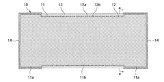
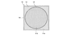
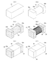
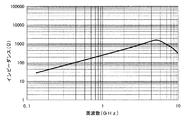
図1〜図8は本発明の第1実施形態を示す。図1はノイズ除去デバイスの長さ方向に沿う縦断面図、図2は図1のa−a線断面図、図3〜図7は図1に示したノイズ除去デバイスの製法説明図、図8は図1に示したノイズ除去デバイスのインピーダンス特性図である。 1 to 8 show a first embodiment of the present invention. 1 is a longitudinal sectional view along the length direction of the noise removing device, FIG. 2 is a sectional view taken along the line aa of FIG. 1, FIGS. 3 to 7 are explanatory diagrams of the manufacturing method of the noise removing device shown in FIG. FIG. 2 is an impedance characteristic diagram of the noise removal device shown in FIG. 1.
まず、図1及び図2を引用してノイズ除去デバイスの構造について説明する。図中の10はデバイス、11は柱状コア、12は導体膜、13は外装、14は1対の外部電極である。 First, the structure of the noise removal device will be described with reference to FIGS. In the figure, 10 is a device, 11 is a columnar core, 12 is a conductor film, 13 is an exterior, and 14 is a pair of external electrodes.
柱状コア11は透磁率の共鳴周波数が100MHz以上である磁性絶縁材から成る。ここでの共鳴周波数とは、μ=μ’+jμ”(μは透磁率、μ’は磁界に追従できる透磁率の実数成分、jμ”は磁界に追従できず90度遅れる透磁率の虚数成分)の式において透磁率の虚数成分jμ”がピークとなる周波数を指す。
The
透磁率の共鳴周波数が100MHz以上である磁性絶縁材としては、Ni−Zn系スピネルフェライトや、スピネルフェライトよりも共鳴周波数が高いY型またはZ型等の六方晶フェライト等が好適に使用できる。また、焼結性の調整のためにNi−Zn−Cu系スピネルフェライトを用いてもよく、Bi2O3やSiO2 等の添加により焼結性を調整することもできる。さらに、特性の微調整を行うためにCoOやMn2O3やMgOやCr2O3等の酸化物を添加してもよい。 As the magnetic insulating material having a magnetic resonance resonance frequency of 100 MHz or more, Ni-Zn spinel ferrite, Y-type or Z-type hexagonal ferrite having a resonance frequency higher than that of spinel ferrite, and the like can be preferably used. Further, Ni—Zn—Cu based spinel ferrite may be used for adjusting the sinterability, and the sinterability can be adjusted by adding Bi 2 O 3 , SiO 2 or the like. Furthermore, an oxide such as CoO, Mn 2 O 3 , MgO, or Cr 2 O 3 may be added to finely adjust the characteristics.
Ni−Zn系スピネルフェライトはFe比やNi/Zn比等の組成調整により透磁率及び周波数特性を調整可能である。Ni−Zn系スピネルフェライトを使用する場合における好ましいFe比はFe2O3として40mol%以上であるが、Fe比が49.5mol%を越えると損失が大きくなり、且つ、46mol%未満では透磁率が低くなる傾向があることからFe比が46〜49.5mol%の範囲のものを使用することが望ましい。また、共鳴周波数はNi/Zn比で変化可能であり、Ni/Zn比を大きくすることで共鳴周波数を高くすることができる。好ましいNi/Zn比は1以上であるが、Ni/Zn比が4以上のものを使用することが望ましい。 Ni-Zn spinel ferrite can be adjusted in magnetic permeability and frequency characteristics by adjusting the composition such as Fe ratio and Ni / Zn ratio. The preferred Fe ratio in the case of using the Ni-Zn-based spinel ferrite is 40 mol% or more as Fe 2 O 3, loss of Fe ratio exceeds 49.5 mol% is increased, and is less than 46 mol% permeability Therefore, it is desirable to use a material having an Fe ratio in the range of 46 to 49.5 mol%. The resonance frequency can be changed by the Ni / Zn ratio, and the resonance frequency can be increased by increasing the Ni / Zn ratio. A preferable Ni / Zn ratio is 1 or more, but it is desirable to use a Ni / Zn ratio of 4 or more.
尚、柱状コア11を構成する磁性絶縁材には、前記フェライト磁性体粉末またはその他の磁性体粉末を、非磁性の無機絶縁体中または非磁性の有機絶縁体中に所定量含有させた複合磁性体を用いることもできる。因みに、前記透磁率の共鳴周波数が100MHz未端のものでは高周波帯域で十分なインピーダンス特性が得られない。
The magnetic insulating material constituting the
また、柱状コア11は、2つの四角柱部11aを両端に対称に有し、且つ、2つの四角柱部11a間に四角柱部11aよりも外形が小さな円柱部11bを同軸上に有する。2つの四角柱部11aの横断面は正方形またはこれに近似した形状を成し、円柱部11bの横断面は円形またはこれに近似した形状を成す。図面には2つの四角柱部11aと円柱部11bとの境界面を柱状コア11の中心線と直交する面で構成したものを示してあるが、境界面を柱状コア11の中心線と鋭角を成す面、立体的には四角柱部11aから円柱部11bに向かって徐々に外形が小さくなる円錐台状に形成しても構わない。
Further, the
導体膜12は、柱状コア11の軸方向一端から他端に亘って外周面を覆うようにほぼ均一な厚さ、具体的には10〜20μmの厚さで形成されている。この導体膜12の円柱部11b上に存する部分(導体膜12の軸方向中央部分)には所定溝幅の螺旋溝12bがレーザトリミング加工により形成され、該螺旋溝12bにより所定周回数を持つ所定線幅の螺状線部12aが形成されている。
The
この導体膜12はCu,Ni,Ag,Pt等の金属から成り、その抵抗率は1〜5×10⁻⁸Ωmの範囲内にある。また、後に詳述するように、螺状線部12aを構成する線の表面にはレーザトリミング時の溶融飛散物から成る酸化物膜DR(図6(B)参照)が形成されており、該酸化物膜DRは柱状コア11を構成する磁性絶縁材成分を含有している。
The
外装13は、導体膜12の円柱部11b上に存する部分に設けられた螺旋溝12b内に充填され、且つ、螺状線部12aを構成する線の表面を覆うように、しかも、外観形状が四角柱状になるように形成されており、その4つの側面は四角柱部11aの4つの側面とそれぞれ平行またはこれに近似した形態を成す。
The
この外装13は柱状コア11を構成する磁性絶縁材よりも誘電率が小さい磁性絶縁材から成り、具体的にはNi−Zn系スピネルフェライト粉末,Mn−Zn系スピネルフェライト粉末,六方晶フェライト粉末,金属磁性粉末のうちの少なくとも1種をエポキシ樹脂等の絶縁性プラスチック材料に30〜90wt%、好ましくは65wt%含有させた磁性粉末含有プラスチックから成る。前記金属磁性粉末にはパーマロイ,センダスト,純鉄等が好適に使用でき、この場合には外装表面の平滑性を得るために最大粒径が20μm以下のものを用いることが好ましく、より好ましくは金属磁性粉末の表面に酸化膜を形成したものを用いる。
The
1対の外部電極14は、導体膜12の各四角柱部11aの端面及び4つの側面の上に存する部分(導体膜12の軸方向両端部分)の表面を覆い、且つ、外装13を挟むようにほぼ均一な厚さ、具体的には5〜20μmの厚さで形成されている。外装13で覆われた導体膜12の軸方向中央部分(螺状線部12aを含む)への湿気浸入を防止するため、各外部電極14の外装側の端縁は外装13の端縁と接触しており、また、デバイス10を基板等に実装するときのことを考慮し各外部電極14の側面の表面高さは外装13の側面の表面高さよりも若干高くなっている。この外部電極14はAg,Cu,Ni,Sn等の金属及びこれらの合金から成り、単層または多層構造を有する。
The pair of
次に、図3〜図7を引用して図1に示したノイズ除去デバイスの製法について説明する。 Next, a method of manufacturing the noise removal device shown in FIG. 1 will be described with reference to FIGS.
まず、図3(A)に示すような直方体形状の未焼成コア基材21を用意する。具体的には、図4(A)に示すように押出成形等の手法により得た横断面四角形の未焼成セラミック棒M1を部品寸法に見合った長さ寸法で切断する方法によって未焼成コア基材21を形成するか、または、図4(B)に示すようにスクリーン印刷等の手法により得た所定厚さの未焼成セラミックシートM2を部品寸法に見合った幅及び長さ寸法で切断する方法によって未焼成コア基材21を形成する。未焼成セラミックシートM2は単層シートまたは積層シートの何れでもよく、積層シートの場合には複数のシートを積み重ねた後にこれを厚み方向にプレスしたものを用いることが好ましい。また、図示を省略したが、この未焼成コア基材21はその形状に合ったキャビティを有する金型にセラミックスラリーを充填する方法によっても得ることができる。
First, an
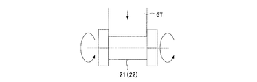
そして、図3(B)に示すように未焼成コア基材21を切削加工して、2つの四角柱部22aを両端に対称に有し、且つ、2つの四角柱部22a間に四角柱部22aよりも外形が小さな円柱部22bを同軸上に有する未焼成柱状コア22を形成する。具体的には、図5に示すように、未焼成コア基材21の長さ方向の両端部を回転可能なホルダー(図示省略)によって保持して所定方向に回転させながらその中央部分を切削刃GTで削り取る方法によって未焼成柱状コア22を形成する。図示を省略したが、この未焼成柱状コア22はその形状に合ったキャビティを有する金型にセラミックスラリーを充填する方法によっても得ることができる。
Then, as shown in FIG. 3B, the unfired
そして、未焼成柱状コア22をその材料成分に応じた熱処理条件で焼成し、焼結後の柱状コア22(便宜上、未焼成柱状コアと同一符号を用いる)に一括でバレル研磨を施す。焼成後のバレル研磨は必ずしも必要なものではないが、バレル研磨によって柱状コア22の稜線位置に存するバリが除去されると共に後述する導体膜23の付着が良くなるように柱状コア22の表面全体が適度に荒らされる。
Then, the
そして、図3(C)に示すように柱状コア22の軸方向一端から他端に亘って外周面を覆うようにほぼ均一な厚さで導体膜23を形成する。この導体膜23の形成にはメッキ法やスパッタリングや蒸着等の薄膜形成手法が適宜利用できる。
Then, as shown in FIG. 3C, the
そして、図3(D)に示すように導体膜23の円柱部22b上に存する部分(導体膜23の軸方向中央部分)に所定溝幅の螺旋溝24をレーザトリミング加工により形成して、該螺旋溝24により所定周回数を持つ所定線幅の螺状線部23aを形成する。具体的には、図6(A)に示すように、導体膜23が形成された柱状コア22の長さ方向の両端部を回転可能なホルダー(図示省略)によって保持して所定方向に回転させ、導体膜23の円柱部22b上に存する部分にYAG等に依るレーザ光LBを柱状コア22をその中心線方向に相対的に移動させながら照射してレーザ光照射箇所を溶融消失させる方法によって螺旋溝24及び螺状線部23aを形成する。このレーザトリミング加工により導体膜23の円柱部22b上に存する部分には螺旋溝24の形成ピッチに合致した螺状線部23aが形成されるが、螺状線部23aの線幅w1と螺旋溝24の溝幅w2は照射レーザ光のスポット径並びに前記相対移動量によって任意にコントロールできる(図6(B)参照)。
Then, as shown in FIG. 3 (D), a
また、レーザトリミング加工時には、導体膜23のレーザ光照射箇所のみならずその下側の柱状コア22の一部も加熱溶融され、その溶融飛散物から成る酸化物膜(ドロス)DRが螺状線部23aを構成する線の表面及び溝の表面を覆うように、不均等ではあるが概ね0.2〜5.0μmの厚みで付着する(図6(B)参照)。溶融飛散物から成る酸化物膜DRは主として柱状コア22を構成する磁性絶縁材成分及びその酸化物であるが、導体膜23を構成する金属成分及びその酸化物も少量含まれることもあり得る。
Further, at the time of laser trimming, not only the portion of the
図6(B)には螺状線部23aを構成する線の表面全体に且つその幅方向両端に肉厚部分が存するように酸化物膜DRが形成されたものを示してあるが、酸化物膜DRの形態はこれに限定されるものではなく、螺状線部23aを構成する線の側面から上面に至る肩部分の表面を少なくとも覆うように酸化物膜DRが形成されていれば外部応力から保護が行えると共に後述のインピーダンス底上げ効果も得られる。
FIG. 6B shows an oxide film DR formed on the entire surface of the line constituting the
螺状線部23aを構成する線の表面に溶融飛散物から成る酸化物膜DRを好適に形成するには、比較的弱いレーザ出力で多数回に分けてレーザ光を照射するのが好ましく、例えばレーザ光LBとして波長1.06μmで発振周波数3〜30kHzのYAGレーザ光を使用し、レーザスポット径に対するオーバーラップ比を50〜90%に設定するとよい。
In order to suitably form the oxide film DR made of the molten scattered matter on the surface of the line constituting the
そして、図3(E)に示すように導体膜23の円柱部22b上に存する部分に設けられた螺旋溝24内に充填され、且つ、螺状線部23aを構成する線の表面を覆うように、しかも、外観形状が四角柱状になるように外装25を形成する。具体的には、図7(A)及び図7(B)に示すように、螺状線部23aが形成された柱状コア22の長さ方向の両端部を回転可能なホルダー(図示省略)によって保持して所定方向に回転させながら導体膜33の円柱部22b上に存する部分に塗布ローラARを接触させて柱状コア22を構成する磁性絶縁材よりも誘電率が小さい磁性絶縁材ペーストPPを塗布し、指触乾燥後の硬化過程で整形板FTを押し当てて磁性絶縁材ペーストPPの外観形状を四角柱状に整形する方法によって外装25を形成する。外装用の磁性絶縁材ペーストPPに含まれる絶縁性プラスチック材料として熱硬化性のものを用いる場合は熱付与により硬化過程が実施され、紫外線等の光硬化性のものを用いる場合は光照射により硬化過程が実施される。
Then, as shown in FIG. 3E, the
そして、図3(F)に示すように導体膜23の各四角柱部22aの端面及び4つの側面の上に存する部分(導体膜23の軸方向両端部分)の表面を覆い、且つ、外装25を挟むようにほぼ均一な厚さで外部電極26を形成する。この外部電極26の形成には電解メッキ等の薄膜形成手法が適宜利用できる。
Then, as shown in FIG. 3 (F), the surfaces of the end portions and the four side surfaces of the respective
次に、図8を引用して図1に示したノイズ除去デバイスのインピーダンス特性について説明する。因みに、図中の実線は、図1に示したデバイス10の構造にあって柱状コア11としてFe2O3を47mol%,NiOを40mol%,ZnOを2mol%,CuOを6mol%の組成比としたNi−Zn系スピネルフェライト(透磁率の共鳴周波数が100MHz以上の磁性絶縁材)を用い、且つ、外装13としてNi−Zn系スピネルフェライト粉末を65%含有したエポキシ樹脂を用いた場合のインピーダンス特性である。
Next, the impedance characteristics of the noise removal device shown in FIG. 1 will be described with reference to FIG. Incidentally, the solid line in the figure shows the composition ratio of the
図8から分かるように、このデバイスは、特定の周波数帯域でのみ他の周波数帯域に比べて遥かに高いインピーダンスを生じる特性を有するものではなく、4.5GHz付近をピークとして数百MHz〜数GHzの広帯域においてなだらかな勾配を示すインピーダンス特性を有することから、1個のデバイスで広い周波数帯域において狙い通りのノイズ除去効果を安定して得ることが可能である。とりわけ、携帯電話の使用周波数帯域である800MHz,1.5GHz,1.9GHz及び2.0GHzにあっては全帯域において高インピーダンスが得られることからこれら帯域において優れたノイズ除去効果を得ることができる。 As can be seen from FIG. 8, this device does not have a characteristic that produces a much higher impedance than the other frequency bands only in a specific frequency band, and it is several hundred MHz to several GHz with a peak around 4.5 GHz. Therefore, it is possible to stably obtain a desired noise removal effect in a wide frequency band with a single device. In particular, since high impedance is obtained in all bands at 800 MHz, 1.5 GHz, 1.9 GHz and 2.0 GHz which are the frequency bands used by mobile phones, an excellent noise removal effect can be obtained in these bands. .
前記のようなインピーダンス特性が現れる根拠は定かではないが、デバイス10自体の基本構造が関与していることに加え、螺状線部12aを構成する線の側面から上面に至る肩部分に少なくとも形成された酸化物膜DRの存在が大きく影響していると考えられる。この酸化物膜DRは主として柱状コア11を構成する磁性絶縁材成分及びその酸化物であるため、該酸化物膜DRの存在によって螺状線部12aを構成する線の表面抵抗が増加し、これによりインピーダンスが底上げされて前記のような特性が現れるものと推測される。
The reason why the impedance characteristic as described above appears is not clear, but in addition to the basic structure of the
また、柱状コア11の螺状線部12aが設けられた部分(円柱部11b)の柱状コア11の軸と直交する断面形状を円形とすることで、浮遊容量が低減でき、しかも、高周波帯域において良好なノイズ除去効果が得られるものと推測される。
Further, by making the cross-sectional shape perpendicular to the axis of the
図9は本発明の第2実施形態を示すノイズ除去デバイスの製法説明図である。 FIG. 9 is an explanatory diagram of a method of manufacturing a noise removing device according to the second embodiment of the present invention.
図9(F)に示すノイズ除去デバイス30が図1に示したノイズ除去デバイス10と構造上で異なるところは、図9(B)に示すように柱状コア32が2つの四角柱部32aを両端に対称に有し、且つ、2つの四角柱部32a間に四角柱部32aよりも外形が小さな四角柱部32bを同軸上に有する点にある。
The
このノイズ除去デバイス30を製造するときには、まず、図9(A)に示すような直方体形状の未焼成コア基材31を用意する。具体的には、図4(A)に示した方法と同様に押出成形等の手法により得た横断面四角形の未焼成セラミック棒M1を部品寸法に見合った長さ寸法で切断する方法によって未焼成コア基材31を形成するか、または、図4(B)に示した方法と同様にスクリーン印刷等の手法により得た所定厚さの未焼成セラミックシートM2を部品寸法に見合った幅及び長さ寸法で切断する方法によって未焼成コア基材31を形成する。未焼成セラミックシートは単層シートまたは積層シートの何れでもよく、積層シートの場合には複数のシートを積み重ねた後にこれを厚み方向にプレスしたものを用いることが好ましい。また、図示を省略したが、この未焼成コア基材31はその形状に合ったキャビティを有する金型にセラミックスラリーを充填する方法によっても得ることができる。
When manufacturing the
そして、図9(B)に示すように未焼成コア基材31を切削加工して、2つの四角柱部32aを両端に対称に有し、且つ、2つの四角柱部32a間に四角柱部32aよりも外形が小さな四角柱部32bを同軸上に有する未焼成柱状コア32を形成する。具体的には、未焼成コア基材31の長さ方向の両端部を回転可能なホルダーによって保持してその中央部分を切削刃で側面と平行に削り取る方法を90度向きを変えながら実施することによって未焼成柱状コア32を形成する。図示を省略したが、この未焼成柱状コア32はその形状に合ったキャビティを有する金型にセラミックスラリーを充填する方法によっても得ることができる。
Then, as shown in FIG. 9 (B), the unfired
そして、未焼成柱状コア32をその材料成分に応じた熱処理条件で焼成し、焼結後の柱状コア32(便宜上、未焼成柱状コアと同一符号を用いる)に一括でバレル研磨を施す。焼成後のバレル研磨は必ずしも必要なものではないが、バレル研磨によって柱状コア32の稜線位置に存するバリが除去されると共に後述する導体膜33の付着が良くなるように柱状コア32の表面全体が適度に荒らされる。
Then, the
そして、図9(C)に示すように柱状コア32の軸方向一端から他端に亘って外周面を覆うようにほぼ均一な厚さで導体膜33を形成する。この導体膜33の形成にはメッキ法やスパッタリング等の薄膜形成手法が適宜利用できる。
Then, as shown in FIG. 9C, the
そして、図9(D)に示すように導体膜33の四角柱部32b上に存する部分(導体膜23の軸方向中央部分)に所定溝幅の螺旋溝34をレーザトリミング加工により形成して、該螺旋溝34により所定周回数を持つ所定線幅の螺状線部33aを形成する。具体的には、図6(A)に示した方法と同様に、導体膜33が形成された柱状コア32の長さ方向の両端部を回転可能なホルダー(図示省略)によって保持して所定方向に回転させ、四角部32b上に存する導体膜33にYAG等に依るレーザ光LBを柱状コア32をその中心線方向に相対的に移動させながら照射してレーザ光照射箇所を溶融消失させる方法によって螺旋溝34及び螺状線部33aを形成する。このレーザトリミング加工により導体膜33の四角柱部32b上に存する部分には螺旋溝34の形成ピッチに合致した螺状線部33aが形成されるが、螺状線部33aの線幅と螺旋溝34の溝幅は照射レーザ光のスポット径並びに前記相対移動量によって任意にコントロールすることができる。
Then, as shown in FIG. 9D, a
また、レーザトリミング加工時には、導体膜33のレーザ光照射箇所のみならずその下側の柱状コア32の一部も加熱溶融され、その溶融飛散物から成る酸化物膜(ドロス)DRが螺状線部33aを構成する線の表面及び溝の表面を覆うように、不均等ではあるが概ね0.2〜5.0μmの厚みで付着する(図6(B)参照)。溶融飛散物から成る酸化物膜DRは主として柱状コア11を構成する磁性絶縁材成分及びその酸化物であるが、導体膜23を構成する金属成分及びその酸化物も少量含まれることもあり得る。この酸化物膜DRの形態及び好適な形成手法は第1実施形態で述べたものと同じである。
Further, at the time of laser trimming, not only the portion of the
前記のレーザトリミング加工では、レーザ光照射によって導体膜33の四角柱部32b上に存する部分に螺旋溝34及び螺状線部33aを形成するため、螺状線部33aにおける四角柱部32bの4つの稜線及びその近傍部分に存する線の幅が4つの平面部分に存する線の幅よりも細くなって断線の原因となる恐れがあるが、同恐れは4つの稜線及びその近傍部分に存する線の表面を覆う酸化物膜DRの厚みを4つの平面部分の線の表面を覆う酸化物膜DRの厚みよりも厚くして該酸化物膜DRによって線の補強を行うことにより防止することが可能である。因みに、4つの稜線及びその近傍部分に存する線の表面を覆う酸化物膜DRの厚みを厚くするには、導体膜33の四角柱部32b上に存する部分にレーザ光LBを照射するときの角度を90度よりも小さくし同部分とレーザ光LBの焦点との距離を大きくとることによって同部分へのレーザ光LBの照射強度を弱め、強度の弱いレーザ光LBによって導体膜33の四角柱部32b上に存する部分をゆっくりと熱することによって溶融飛散物の量を増加させる方法が採用できる。また、照射強度の弱いレーザ光LBが導体膜33の四角柱部32b上に存する部分に照射されるようにレーザ発振器側または光学系側で照射強度を可変する方法も採用できる。
In the laser trimming process, the
そして、図9(E)に示すように導体膜33の四角柱部32b上に存する部分に設けられた螺旋溝34内に充填され、且つ、螺状線部33aを構成する線の表面を覆うように、しかも、外観形状が四角柱状になるように外装35を形成する。具体的には、図7(A)及び図7(B)で示した方法と同様に、螺状線部33aが形成された柱状コア32の長さ方向の両端部を回転可能なホルダー(図示省略)によって保持して所定方向に回転させながら導体膜33の円柱部32b上に存する部分に塗布ローラARを接触させて柱状コア32を構成する磁性絶縁材よりも誘電率が小さい磁性絶縁材ペーストPPを塗布し、指触乾燥後の硬化過程で整形板FTを押し当てて磁性絶縁材ペーストPPの外観形状を四角柱状に整形する方法によって外装35を形成する。外装用の磁性絶縁材ペーストPPに含まれる絶縁性プラスチック材料として熱硬化性のものを用いる場合は熱付与により硬化過程が実施され、紫外線等の光硬化性のものを用いる場合は光照射により硬化過程が実施される。
Then, as shown in FIG. 9E, the
そして、図9(F)に示すように導体膜33の各四角柱部32aの端面及び4つの側面の上に存する部分(導体膜33の軸方向両端部分)の表面を覆い、且つ、外装35を挟むようにほぼ均一な厚さで外部電極36を形成する。この外部電極36の形成には電解メッキ等の薄膜形成手法が適宜利用できる。
Then, as shown in FIG. 9 (F), the surfaces of the end portions and the four side surfaces of the
このようにして製造されたノイズ除去デバイス30にあっても、構造上で若干の相違はあるものの、図1に示したノイズ除去デバイス10と同様の作用効果を得ることができる。
Even in the
図10は本発明の第3実施形態を示すノイズ除去デバイスの製法説明図である。 FIG. 10 is an explanatory diagram of a method of manufacturing a noise removing device according to the third embodiment of the present invention.
図10(F)に示すノイズ除去デバイス40が図1に示したノイズ除去デバイスと構造上で異なるところは、図9(D)に示す柱状コア44が全体として四角柱状である点にある。
The
このノイズ除去デバイス40を製造するときには、まず、図10(A)に示すような所定長を有する直方体形状の未焼成コア基材41を用意する。具体的には、図4(A)に示した方法と同様に押出成形等の手法により得た横断面四角形の未焼成セラミック棒M1を所定の長さ寸法で切断する方法によって未焼成コア基材41を形成するか、または、図4(B)に示した方法と同様にスクリーン印刷等の手法により得た所定厚さの未焼成セラミックシートM2を所定の幅及び長さ寸法で切断する方法によって未焼成コア基材41を形成する。未焼成セラミックシートは単層シートまたは積層シートの何れでもよく、積層シートの場合には複数のシートを積み重ねた後にこれを厚み方向にプレスしたものを用いることが好ましい。また、図示を省略したが、この未焼成コア基材41はその形状に合ったキャビティを有する金型にセラミックスラリーを充填する方法によっても得ることができる。
When manufacturing the
そして、未焼成コア基材41をその材料成分に応じた熱処理条件で焼成し、焼結後のコア基材41(便宜上、未焼成コア基材と同一符号を用いる)に一括でバレル研磨を施す。焼成後のバレル研磨は必ずしも必要なものではないが、バレル研磨によってコア基材41の稜線位置に存するバリが除去されると共に後述する導体膜42の付着が良くなるようにコア基材41の表面全体が適度に荒らされる。
Then, the unfired
そして、図10(B)に示すようにコア基材41の表面全体を覆うようにほぼ均一な厚さで導体膜42を形成する。この導体膜42の形成にはメッキ法やスパッタリングや蒸着等の薄膜形成手法が適宜利用できる。
Then, as shown in FIG. 10B, the
そして、図10(C)に示すようにコア基材41の表面に存する導体膜43に所定溝幅の螺旋溝43をレーザトリミング加工により等間隔で形成して、該螺旋溝43により所定周回数を持つ所定線幅の螺状線部42aを等間隔で形成する。具体的には、図6(A)に示した方法と同様に、導体膜42が形成されたコア基材41の長さ方向の両端部を回転可能なホルダー(図示省略)によって保持して所定方向に回転させ、導体膜42にYAG等に依るレーザ光LBをコア基材41をその中心線方向に相対的に移動させながら照射してレーザ光照射箇所を溶融消失させる方法によって螺旋溝43及び螺状線部42aを等間隔で形成する。このレーザトリミング加工により導体膜42には螺旋溝43の形成ピッチに合致した螺状線部42aが形成されるが、螺状線部42aの線幅と螺旋溝43の溝幅は照射レーザ光のスポット径並びに前記相対移動量によって任意にコントロールすることができる。
Then, as shown in FIG. 10C,
また、レーザトリミング加工時には、導体膜42のレーザ光照射箇所のみならずその下側のコア基材41の一部も加熱溶融され、その溶融飛散物から成る酸化物膜(ドロス)DRが螺状線部42aを構成する線の表面及び溝の表面を覆うように、不均等ではあるが概ね0.2〜5.0μmの厚みで付着する(図6(B)参照)。溶融飛散物から成る酸化物膜DRは主としてコア機材41を構成する磁性絶縁材成分及びその酸化物であるが、導体膜42を構成する金属成分及びその酸化物も少量含まれることもあり得る。この酸化物膜DRの形態及び好適な形成手法は第1実施形態で述べたものと同じである。
Further, at the time of laser trimming, not only the portion of the
また、レーザトリミング加工時には、必要に応じて第2の実施形態で述べたレーザ照射方法を採用することにより、螺状線部42aにおける4つの稜線及びその近傍部分に存する線の表面を覆う酸化物膜DRの厚みを厚くして該酸化物膜DRによって線の補強を行う。
Further, at the time of laser trimming, an oxide that covers the surfaces of the four ridge lines in the
そして、図10(D)に示すように螺旋溝43及び螺状線部42aを形成した後のコア基材41を部品寸法に見合った長さ寸法で切断して1部品に対応する柱状コア44を形成する。
Then, as shown in FIG. 10 (D), the
そして、図10(E)に示すように柱状コア44の螺旋溝43内に充填され、且つ、螺状線42aを構成する線の表面を覆うように、しかも、外観形状が四角柱状になるように外装45を形成する。具体的には、図7(A)及び図7(B)に示した方法と同様に、柱状コア44の長さ方向の両端部を回転可能なホルダー(図示省略)によって保持して所定方向に回転させながら螺状線部42aに塗布ローラARを接触させて柱状コア44を構成する磁性絶縁材よりも誘電率が小さい磁性絶縁材ペーストPPを塗布し、指触乾燥後の硬化過程で整形板FTを押し当てて磁性絶縁材ペーストPPの外観形状を四角柱状に整形する方法によって外装45を形成する。外装用の磁性絶縁材ペーストPPに含まれる絶縁性プラスチック材料として熱硬化性のものを用いる場合は熱付与により硬化過程が実施され、紫外線等の光硬化性のものを用いる場合は光照射により硬化過程が実施される。
Then, as shown in FIG. 10 (E), the
そして、図10(F)に示すように導体膜42の両端部分の表面を覆い、且つ、外装45を挟むようにほぼ均一な厚さで外部電極46を形成する。この外部電極46の形成には電解メッキ等の薄膜形成手法が適宜利用できる。
Then, as shown in FIG. 10F, the
このようにして製造されたノイズ除去デバイス40にあっても、構造上で若干の相違はあるものの、図1に示したノイズ除去デバイス10と同様の作用効果を得ることができる。
Even in the
10…ノイズ除去デバイス、11…柱状コア、11a…四角柱部、11b…円柱部、12…導体膜、12a…螺状線部、12b…螺旋溝、13…外装、14…外部電極、20,30…ノイズ除去デバイス。
DESCRIPTION OF
Claims (4)
柱状コアの外周面にその軸方向一端から他端に亘って形成された導体膜と、
導体膜の軸方向中央部分に螺旋溝をレーザトリミング加工することによって形成された所定周回数を持つ螺状線部と、
螺状線部を構成する線の側面から上面に至る肩部分の表面を少なくとも覆うように形成された酸化物膜と、
第1の磁性絶縁材よりも誘電率が小さい第2の磁性絶縁材から成り、導体膜の軸方向中央部分の螺旋溝内に充填され、且つ、螺状線部を構成する線の表面を覆うように形成された外装と、
導体膜の軸方向両端部分に外装を挟むように形成された1対の外部電極とを備える、
ことを特徴とするノイズ除去デバイス。 A columnar core made of a first magnetic insulating material having a resonance frequency of permeability of 100 MHz or more;
A conductor film formed on the outer peripheral surface of the columnar core from one end to the other in the axial direction;
A spiral wire portion having a predetermined number of turns formed by laser trimming a spiral groove in an axially central portion of the conductor film;
An oxide film formed so as to cover at least the surface of the shoulder portion extending from the side surface to the upper surface of the line constituting the spiral line portion;
It consists of the 2nd magnetic insulation material whose dielectric constant is smaller than a 1st magnetic insulation material, is filled in the spiral groove of the axial direction center part of a conductor film, and covers the surface of the line | wire which comprises a helical wire part An exterior formed as follows,
A pair of external electrodes formed so as to sandwich the exterior at both ends in the axial direction of the conductor film,
A noise removing device characterized by that.
ことを特徴とする請求項1に記載のノイズ除去デバイス。 The resistivity of the conductor film is in the range of 1-5 × 10 −8 Ωm.
The noise removal device according to claim 1.
ことを特徴とする請求項1または2に記載のノイズ除去デバイス。 The oxide film is composed of a molten scattered material at the time of laser trimming, and the molten scattered material contains a first magnetic insulating material component.
The noise removal device according to claim 1 or 2, characterized in that
ことを特徴とする請求項1〜3の何れか1項に記載のノイズ除去デバイス。 The outer package is made of a magnetic powder-containing plastic containing 30 to 90 wt% of at least one of Ni—Zn ferrite powder, Mn—Zn ferrite powder, hexagonal ferrite powder, and metal magnetic powder.
The noise removal device according to any one of claims 1 to 3, wherein
Priority Applications (2)
| Application Number | Priority Date | Filing Date | Title |
|---|---|---|---|
| JP2004287085A JP2006100697A (en) | 2004-09-30 | 2004-09-30 | Noise rejection device |
| US11/241,568 US7170379B2 (en) | 2004-09-30 | 2005-09-29 | Noise rejection device and cellular phone including the noise rejection device |
Applications Claiming Priority (1)
| Application Number | Priority Date | Filing Date | Title |
|---|---|---|---|
| JP2004287085A JP2006100697A (en) | 2004-09-30 | 2004-09-30 | Noise rejection device |
Publications (1)
| Publication Number | Publication Date |
|---|---|
| JP2006100697A true JP2006100697A (en) | 2006-04-13 |
Family
ID=36240187
Family Applications (1)
| Application Number | Title | Priority Date | Filing Date |
|---|---|---|---|
| JP2004287085A Pending JP2006100697A (en) | 2004-09-30 | 2004-09-30 | Noise rejection device |
Country Status (2)
| Country | Link |
|---|---|
| US (1) | US7170379B2 (en) |
| JP (1) | JP2006100697A (en) |
Cited By (2)
| Publication number | Priority date | Publication date | Assignee | Title |
|---|---|---|---|---|
| JPWO2018029998A1 (en) * | 2016-08-09 | 2019-06-06 | パナソニックIpマネジメント株式会社 | Common mode choke coil and method of manufacturing the same |
| JP2021163859A (en) * | 2020-03-31 | 2021-10-11 | 株式会社村田製作所 | Inductor |
Families Citing this family (5)
| Publication number | Priority date | Publication date | Assignee | Title |
|---|---|---|---|---|
| JP2006100700A (en) * | 2004-09-30 | 2006-04-13 | Chuki Seiki Kk | Noise rejection device |
| JP2008306017A (en) * | 2007-06-08 | 2008-12-18 | Citizen Electronics Co Ltd | Inductor and its manufacturing method |
| US11355276B2 (en) * | 2009-02-27 | 2022-06-07 | Cyntec Co., Ltd. | Choke |
| KR20170023501A (en) * | 2015-08-24 | 2017-03-06 | 삼성전기주식회사 | Coil electronic component and manufacturing method thereof |
| DE102022111363A1 (en) * | 2022-05-06 | 2023-11-09 | Tdk Electronics Ag | Inductive filter element |
Citations (7)
| Publication number | Priority date | Publication date | Assignee | Title |
|---|---|---|---|---|
| JP2000243629A (en) * | 1998-12-21 | 2000-09-08 | Murata Mfg Co Ltd | Inductor and manufacture thereof |
| JP2001326120A (en) * | 2000-03-10 | 2001-11-22 | Alps Electric Co Ltd | Inductive device and dc-dc converter using the same |
| JP2002015926A (en) * | 2000-06-30 | 2002-01-18 | Matsushita Electric Ind Co Ltd | Inductance element and manufacturing method |
| JP2003002656A (en) * | 2001-04-09 | 2003-01-08 | Toda Kogyo Corp | Soft magnetic hexagonal ferrite composite particle powder, green sheet using the same, and soft magnetic hexagonal ferrite sintered body |
| JP2003188037A (en) * | 2001-12-14 | 2003-07-04 | Murata Mfg Co Ltd | Manufacturing method for coil component |
| JP2003297636A (en) * | 2002-04-03 | 2003-10-17 | Matsushita Electric Ind Co Ltd | Coil parts |
| JP2003297642A (en) * | 2002-04-02 | 2003-10-17 | Tdk Corp | Chip inductor and its manufacturing method |
Family Cites Families (6)
| Publication number | Priority date | Publication date | Assignee | Title |
|---|---|---|---|---|
| GB2214240A (en) * | 1988-01-06 | 1989-08-31 | Laurence Patrick Wettern | Wine aeration pump |
| US6144280A (en) * | 1996-11-29 | 2000-11-07 | Taiyo Yuden Co., Ltd. | Wire wound electronic component and method of manufacturing the same |
| JP2000156622A (en) | 1998-11-19 | 2000-06-06 | Murata Mfg Co Ltd | Noise suppression component |
| JP4039779B2 (en) * | 1999-01-28 | 2008-01-30 | 太陽誘電株式会社 | Manufacturing method of chip-shaped electronic component |
| JP2001326122A (en) * | 2000-03-10 | 2001-11-22 | Murata Mfg Co Ltd | Multilayer inductor |
| JP2002008931A (en) * | 2000-04-18 | 2002-01-11 | Taiyo Yuden Co Ltd | Wound type common-mode choke coil |
-
2004
- 2004-09-30 JP JP2004287085A patent/JP2006100697A/en active Pending
-
2005
- 2005-09-29 US US11/241,568 patent/US7170379B2/en not_active Expired - Fee Related
Patent Citations (7)
| Publication number | Priority date | Publication date | Assignee | Title |
|---|---|---|---|---|
| JP2000243629A (en) * | 1998-12-21 | 2000-09-08 | Murata Mfg Co Ltd | Inductor and manufacture thereof |
| JP2001326120A (en) * | 2000-03-10 | 2001-11-22 | Alps Electric Co Ltd | Inductive device and dc-dc converter using the same |
| JP2002015926A (en) * | 2000-06-30 | 2002-01-18 | Matsushita Electric Ind Co Ltd | Inductance element and manufacturing method |
| JP2003002656A (en) * | 2001-04-09 | 2003-01-08 | Toda Kogyo Corp | Soft magnetic hexagonal ferrite composite particle powder, green sheet using the same, and soft magnetic hexagonal ferrite sintered body |
| JP2003188037A (en) * | 2001-12-14 | 2003-07-04 | Murata Mfg Co Ltd | Manufacturing method for coil component |
| JP2003297642A (en) * | 2002-04-02 | 2003-10-17 | Tdk Corp | Chip inductor and its manufacturing method |
| JP2003297636A (en) * | 2002-04-03 | 2003-10-17 | Matsushita Electric Ind Co Ltd | Coil parts |
Cited By (5)
| Publication number | Priority date | Publication date | Assignee | Title |
|---|---|---|---|---|
| JPWO2018029998A1 (en) * | 2016-08-09 | 2019-06-06 | パナソニックIpマネジメント株式会社 | Common mode choke coil and method of manufacturing the same |
| US11069468B2 (en) | 2016-08-09 | 2021-07-20 | Panasonic Intellectual Property Management Co., Ltd. | Common mode choke coil and manufacturing method therefor |
| JP7012221B2 (en) | 2016-08-09 | 2022-01-28 | パナソニックIpマネジメント株式会社 | Manufacturing method of common mode choke coil |
| JP2021163859A (en) * | 2020-03-31 | 2021-10-11 | 株式会社村田製作所 | Inductor |
| JP7456239B2 (en) | 2020-03-31 | 2024-03-27 | 株式会社村田製作所 | inductor |
Also Published As
| Publication number | Publication date |
|---|---|
| US7170379B2 (en) | 2007-01-30 |
| US20060125587A1 (en) | 2006-06-15 |
Similar Documents
| Publication | Publication Date | Title |
|---|---|---|
| JP2006100700A (en) | Noise rejection device | |
| US11842833B2 (en) | Coil component | |
| US11776727B2 (en) | Coil component magnetic base | |
| US20180182537A1 (en) | Electronic component | |
| KR101370959B1 (en) | Wire-wound inductor | |
| US10811183B2 (en) | Coil component | |
| US10867744B2 (en) | Coil component | |
| KR102148317B1 (en) | Coil component | |
| JP6683183B2 (en) | Laminated coil parts | |
| KR101981615B1 (en) | Coil component | |
| KR102279305B1 (en) | Coil component | |
| US10804022B2 (en) | Coil component | |
| KR101037288B1 (en) | Multilayer Inductors and Manufacturing Methods | |
| JP7371423B2 (en) | coil parts | |
| CN108735431B (en) | Coil component | |
| US11011298B2 (en) | Coil component | |
| US20180308629A1 (en) | Coil component | |
| US20190228899A1 (en) | Method of manufacturing electronic component and electronic component | |
| KR101616610B1 (en) | Multilayered electronic component and manufacturing method thereof | |
| JP2018098489A (en) | Inductor | |
| JP2006100697A (en) | Noise rejection device | |
| JP2021057469A (en) | Electronic component | |
| JP2000243629A (en) | Inductor and manufacture thereof | |
| JP6387697B2 (en) | Magnetic core and coil device | |
| CN111986878A (en) | Laminated coil component |
Legal Events
| Date | Code | Title | Description |
|---|---|---|---|
| A621 | Written request for application examination |
Free format text: JAPANESE INTERMEDIATE CODE: A621 Effective date: 20070809 |
|
| A977 | Report on retrieval |
Free format text: JAPANESE INTERMEDIATE CODE: A971007 Effective date: 20100118 |
|
| A131 | Notification of reasons for refusal |
Free format text: JAPANESE INTERMEDIATE CODE: A131 Effective date: 20100122 |
|
| A02 | Decision of refusal |
Free format text: JAPANESE INTERMEDIATE CODE: A02 Effective date: 20100518 |