JP2006111908A - ダイヤモンド層の形成方法と、それを利用する多層硬質炭素膜の形成方法 - Google Patents
ダイヤモンド層の形成方法と、それを利用する多層硬質炭素膜の形成方法 Download PDFInfo
- Publication number
- JP2006111908A JP2006111908A JP2004299000A JP2004299000A JP2006111908A JP 2006111908 A JP2006111908 A JP 2006111908A JP 2004299000 A JP2004299000 A JP 2004299000A JP 2004299000 A JP2004299000 A JP 2004299000A JP 2006111908 A JP2006111908 A JP 2006111908A
- Authority
- JP
- Japan
- Prior art keywords
- layer
- diamond
- vacuum chamber
- forming
- diamond layer
- Prior art date
- Legal status (The legal status is an assumption and is not a legal conclusion. Google has not performed a legal analysis and makes no representation as to the accuracy of the status listed.)
- Granted
Links
Images

Landscapes
- Chemical Vapour Deposition (AREA)
- Other Surface Treatments For Metallic Materials (AREA)
Abstract
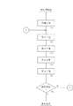
【解決手段】被処理物体の表面に中間層を形成する第1工程と、炭化水素と水素とを真空槽に導入して中間層上にナノダイヤモンド層を形成する第2工程と、水素を真空槽に導入し、ナノダイヤモンド層をダイヤモンド層に成長させる第3工程と、ダイヤモンド層上にダイヤモンドライクカーボン層を形成する第4工程とを繰り返し実行する。
【選択図】図1
Description
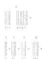
1…中間層
2…ナノダイヤモンド層
3…ダイヤモンド層
4…ダイヤモンドライクカーボン層
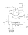
11…真空槽
特許出願人 独立行政法人 科学技術振興機構
石川県
株式会社 オンワード技研
作 道 訓 之
代理人 弁理士 松 田 忠 秋
Claims (5)
- 真空槽に収容する被処理物体の表面に中間層を形成する第1工程と、炭化水素と水素とを真空槽に導入して中間層上にナノダイヤモンド層を形成する第2工程と、水素を真空槽に導入し、ナノダイヤモンド層をダイヤモンド層に成長させる第3工程とからなるダイヤモンド層の形成方法。
- 第3工程において、水素をラジカル化して供給することを特徴とする請求項1記載のダイヤモンド層の形成方法。
- 第1、2工程において、被処理物体に負のパルス電圧を印加することを特徴とする請求項1または請求項2記載のダイヤモンド層の形成方法。
- 第1、2工程を統合して実行することを特徴とする請求項1ないし請求項3のいずれか記載のダイヤモンド層の形成方法。
- 真空槽に収容する被処理物体の表面に多層硬質炭素膜を形成するに際し、請求項1ないし請求項4のいずれか記載のダイヤモンド層の形成方法に加えて、炭化水素を真空槽に導入してダイヤモンド層上にダイヤモンドライクカーボン層を形成する第4工程を付加し、第1〜4工程を繰り返し実行することを特徴とする多層硬質炭素膜の形成方法。
Priority Applications (1)
| Application Number | Priority Date | Filing Date | Title |
|---|---|---|---|
| JP2004299000A JP4813040B2 (ja) | 2004-10-13 | 2004-10-13 | ダイヤモンド層の形成方法と、それを利用する多層硬質炭素膜の形成方法 |
Applications Claiming Priority (1)
| Application Number | Priority Date | Filing Date | Title |
|---|---|---|---|
| JP2004299000A JP4813040B2 (ja) | 2004-10-13 | 2004-10-13 | ダイヤモンド層の形成方法と、それを利用する多層硬質炭素膜の形成方法 |
Publications (2)
| Publication Number | Publication Date |
|---|---|
| JP2006111908A true JP2006111908A (ja) | 2006-04-27 |
| JP4813040B2 JP4813040B2 (ja) | 2011-11-09 |
Family
ID=36380676
Family Applications (1)
| Application Number | Title | Priority Date | Filing Date |
|---|---|---|---|
| JP2004299000A Expired - Fee Related JP4813040B2 (ja) | 2004-10-13 | 2004-10-13 | ダイヤモンド層の形成方法と、それを利用する多層硬質炭素膜の形成方法 |
Country Status (1)
| Country | Link |
|---|---|
| JP (1) | JP4813040B2 (ja) |
Cited By (5)
| Publication number | Priority date | Publication date | Assignee | Title |
|---|---|---|---|---|
| JP2010221353A (ja) * | 2009-03-24 | 2010-10-07 | Mitsubishi Materials Corp | すぐれた仕上げ面精度を示すダイヤモンド被覆工具 |
| JP2010221352A (ja) * | 2009-03-24 | 2010-10-07 | Mitsubishi Materials Corp | 重切削加工においてすぐれた耐摩耗性を発揮するダイヤモンド被覆工具 |
| JP2011098424A (ja) * | 2009-11-09 | 2011-05-19 | Mitsubishi Materials Corp | すぐれた耐欠損性および耐摩耗性を発揮するダイヤモンド被覆工具 |
| WO2014038642A1 (ja) * | 2012-09-07 | 2014-03-13 | ブラザー工業株式会社 | 成膜装置、成膜方法および成膜プログラム |
| US9972476B2 (en) | 2013-03-28 | 2018-05-15 | Brother Kogyo Kabushiki Kaisha | Film forming device, film forming method, and film forming program |
Citations (4)
| Publication number | Priority date | Publication date | Assignee | Title |
|---|---|---|---|---|
| JPH04232273A (ja) * | 1990-08-10 | 1992-08-20 | Norton Co | 超硬質フィルムの多層構造及びその作製方法 |
| JP2001354491A (ja) * | 2000-06-07 | 2001-12-25 | New Japan Radio Co Ltd | ダイヤモンド成長方法及びダイヤモンド成長装置 |
| JP2002293687A (ja) * | 2001-03-29 | 2002-10-09 | Sony Corp | 多結晶性ダイヤモンド薄膜及びその形成方法、半導体装置及びその製造方法、これらの方法の実施に使用する装置、並びに電気光学装置 |
| JP2003155565A (ja) * | 2001-11-19 | 2003-05-30 | Onward Giken:Kk | 多層硬質炭素膜の形成方法と、その装置 |
-
2004
- 2004-10-13 JP JP2004299000A patent/JP4813040B2/ja not_active Expired - Fee Related
Patent Citations (4)
| Publication number | Priority date | Publication date | Assignee | Title |
|---|---|---|---|---|
| JPH04232273A (ja) * | 1990-08-10 | 1992-08-20 | Norton Co | 超硬質フィルムの多層構造及びその作製方法 |
| JP2001354491A (ja) * | 2000-06-07 | 2001-12-25 | New Japan Radio Co Ltd | ダイヤモンド成長方法及びダイヤモンド成長装置 |
| JP2002293687A (ja) * | 2001-03-29 | 2002-10-09 | Sony Corp | 多結晶性ダイヤモンド薄膜及びその形成方法、半導体装置及びその製造方法、これらの方法の実施に使用する装置、並びに電気光学装置 |
| JP2003155565A (ja) * | 2001-11-19 | 2003-05-30 | Onward Giken:Kk | 多層硬質炭素膜の形成方法と、その装置 |
Cited By (6)
| Publication number | Priority date | Publication date | Assignee | Title |
|---|---|---|---|---|
| JP2010221353A (ja) * | 2009-03-24 | 2010-10-07 | Mitsubishi Materials Corp | すぐれた仕上げ面精度を示すダイヤモンド被覆工具 |
| JP2010221352A (ja) * | 2009-03-24 | 2010-10-07 | Mitsubishi Materials Corp | 重切削加工においてすぐれた耐摩耗性を発揮するダイヤモンド被覆工具 |
| JP2011098424A (ja) * | 2009-11-09 | 2011-05-19 | Mitsubishi Materials Corp | すぐれた耐欠損性および耐摩耗性を発揮するダイヤモンド被覆工具 |
| WO2014038642A1 (ja) * | 2012-09-07 | 2014-03-13 | ブラザー工業株式会社 | 成膜装置、成膜方法および成膜プログラム |
| JP2014051715A (ja) * | 2012-09-07 | 2014-03-20 | Nagoya Univ | 成膜装置、成膜方法および成膜プログラム |
| US9972476B2 (en) | 2013-03-28 | 2018-05-15 | Brother Kogyo Kabushiki Kaisha | Film forming device, film forming method, and film forming program |
Also Published As
| Publication number | Publication date |
|---|---|
| JP4813040B2 (ja) | 2011-11-09 |
Similar Documents
| Publication | Publication Date | Title |
|---|---|---|
| JP3962420B2 (ja) | カーボンナノウォールの製造方法、カーボンナノウォールおよび製造装置 | |
| US20070017636A1 (en) | Plasma source and plasma processing apparatus | |
| US20080182027A1 (en) | Synthesis of Carbon Nanotubes by Selectively Heating Catalyst | |
| US20100009242A1 (en) | Carbon nanowall with controlled structure and method for controlling carbon nanowall structure | |
| JP2012041249A (ja) | カーボンナノ構造体の製造方法 | |
| CH694700A5 (de) | Verarbeitungssystem mit doppelten Ionenquellen. | |
| JP4813040B2 (ja) | ダイヤモンド層の形成方法と、それを利用する多層硬質炭素膜の形成方法 | |
| JP2008239357A (ja) | カーボンナノウォールの製造方法 | |
| JP4762945B2 (ja) | カーボンナノウォール構造体 | |
| JP2004270022A (ja) | 薄膜の製造方法および薄膜 | |
| JP4786156B2 (ja) | カーボンナノウォールの製造方法 | |
| Fujita et al. | Structure and resonant characteristics of amorphous carbon pillars grown by focused-ion-beam-induced chemical vapor deposition | |
| JPH04959B2 (ja) | ||
| JPH0917597A (ja) | プラズマ発生装置及び方法 | |
| JP3649873B2 (ja) | Cvd法による薄膜形成方法および薄膜ならびに摺動部品 | |
| JP2005097113A (ja) | カーボンナノウォールの製造方法と製造装置 | |
| Man et al. | Influence of plasma condition on carbon nanotube growth by rf-PECVD | |
| Qian et al. | The effects of magnetic field on the properties of diamond-like carbon films produced by high-density helicon wave plasma | |
| JP2608957B2 (ja) | ダイヤモンド薄膜堆積用基板の製造方法 | |
| JP3246780B2 (ja) | 硬質カーボン膜の形成方法および形成装置 | |
| Panova et al. | Formation of nanostructured carbon on steel targets irradiated by a high-power ion beam | |
| JPH01234397A (ja) | ダイヤモンド状薄膜の製造方法及び装置 | |
| Yamamoto et al. | Plasma states and carbon film deposition in glow discharge connected to dielectric barrier discharge | |
| JP3550665B2 (ja) | 炭化珪素薄膜の製造方法 | |
| JPS63265890A (ja) | ダイヤモンド薄膜又はダイヤモンド状薄膜の製造方法 |
Legal Events
| Date | Code | Title | Description |
|---|---|---|---|
| A621 | Written request for application examination |
Free format text: JAPANESE INTERMEDIATE CODE: A621 Effective date: 20070907 |
|
| A977 | Report on retrieval |
Free format text: JAPANESE INTERMEDIATE CODE: A971007 Effective date: 20100517 |
|
| A131 | Notification of reasons for refusal |
Free format text: JAPANESE INTERMEDIATE CODE: A131 Effective date: 20100601 |
|
| A521 | Written amendment |
Free format text: JAPANESE INTERMEDIATE CODE: A523 Effective date: 20100722 |
|
| A521 | Written amendment |
Free format text: JAPANESE INTERMEDIATE CODE: A821 Effective date: 20100723 |
|
| A131 | Notification of reasons for refusal |
Free format text: JAPANESE INTERMEDIATE CODE: A131 Effective date: 20100921 |
|
| A521 | Written amendment |
Free format text: JAPANESE INTERMEDIATE CODE: A523 Effective date: 20101119 |
|
| TRDD | Decision of grant or rejection written | ||
| A01 | Written decision to grant a patent or to grant a registration (utility model) |
Free format text: JAPANESE INTERMEDIATE CODE: A01 Effective date: 20110809 |
|
| A01 | Written decision to grant a patent or to grant a registration (utility model) |
Free format text: JAPANESE INTERMEDIATE CODE: A01 |
|
| A61 | First payment of annual fees (during grant procedure) |
Free format text: JAPANESE INTERMEDIATE CODE: A61 Effective date: 20110824 |
|
| R150 | Certificate of patent (=grant) or registration of utility model |
Free format text: JAPANESE INTERMEDIATE CODE: R150 |
|
| FPAY | Renewal fee payment (prs date is renewal date of database) |
Free format text: PAYMENT UNTIL: 20140902 Year of fee payment: 3 |
|
| LAPS | Cancellation because of no payment of annual fees |