JP2006150902A - Optical element, optical element molding die and manufacturing method of optical element - Google Patents
Optical element, optical element molding die and manufacturing method of optical element Download PDFInfo
- Publication number
- JP2006150902A JP2006150902A JP2004348660A JP2004348660A JP2006150902A JP 2006150902 A JP2006150902 A JP 2006150902A JP 2004348660 A JP2004348660 A JP 2004348660A JP 2004348660 A JP2004348660 A JP 2004348660A JP 2006150902 A JP2006150902 A JP 2006150902A
- Authority
- JP
- Japan
- Prior art keywords
- optical element
- gate
- cavity
- resin material
- optical
- Prior art date
- Legal status (The legal status is an assumption and is not a legal conclusion. Google has not performed a legal analysis and makes no representation as to the accuracy of the status listed.)
- Pending
Links
- 230000003287 optical effect Effects 0.000 title claims abstract description 328
- 238000000465 moulding Methods 0.000 title claims abstract description 56
- 238000004519 manufacturing process Methods 0.000 title claims abstract description 45
- 229920005989 resin Polymers 0.000 claims abstract description 119
- 239000011347 resin Substances 0.000 claims abstract description 119
- 239000000463 material Substances 0.000 claims abstract description 110
- 238000000034 method Methods 0.000 claims description 11
- 230000007547 defect Effects 0.000 description 23
- 230000000694 effects Effects 0.000 description 8
- 238000001746 injection moulding Methods 0.000 description 4
- 239000002184 metal Substances 0.000 description 4
- 230000000007 visual effect Effects 0.000 description 3
- 239000012778 molding material Substances 0.000 description 2
- 229920000178 Acrylic resin Polymers 0.000 description 1
- 239000004925 Acrylic resin Substances 0.000 description 1
- 239000004697 Polyetherimide Substances 0.000 description 1
- 238000010586 diagram Methods 0.000 description 1
- 238000010438 heat treatment Methods 0.000 description 1
- 238000003384 imaging method Methods 0.000 description 1
- 230000002401 inhibitory effect Effects 0.000 description 1
- 230000002093 peripheral effect Effects 0.000 description 1
- 239000004033 plastic Substances 0.000 description 1
- 229920003023 plastic Polymers 0.000 description 1
- 239000004417 polycarbonate Substances 0.000 description 1
- 229920000515 polycarbonate Polymers 0.000 description 1
- 229920001601 polyetherimide Polymers 0.000 description 1
- 229920005672 polyolefin resin Polymers 0.000 description 1
- 238000007493 shaping process Methods 0.000 description 1
- 239000000243 solution Substances 0.000 description 1
- 229920005992 thermoplastic resin Polymers 0.000 description 1
- 229920001187 thermosetting polymer Polymers 0.000 description 1
Images



Classifications
-
- B—PERFORMING OPERATIONS; TRANSPORTING
- B29—WORKING OF PLASTICS; WORKING OF SUBSTANCES IN A PLASTIC STATE IN GENERAL
- B29C—SHAPING OR JOINING OF PLASTICS; SHAPING OF MATERIAL IN A PLASTIC STATE, NOT OTHERWISE PROVIDED FOR; AFTER-TREATMENT OF THE SHAPED PRODUCTS, e.g. REPAIRING
- B29C45/00—Injection moulding, i.e. forcing the required volume of moulding material through a nozzle into a closed mould; Apparatus therefor
- B29C45/17—Component parts, details or accessories; Auxiliary operations
- B29C45/26—Moulds
- B29C45/27—Sprue channels ; Runner channels or runner nozzles
- B29C45/2701—Details not specific to hot or cold runner channels
- B29C45/2708—Gates
-
- B—PERFORMING OPERATIONS; TRANSPORTING
- B29—WORKING OF PLASTICS; WORKING OF SUBSTANCES IN A PLASTIC STATE IN GENERAL
- B29D—PRODUCING PARTICULAR ARTICLES FROM PLASTICS OR FROM SUBSTANCES IN A PLASTIC STATE
- B29D11/00—Producing optical elements, e.g. lenses or prisms
- B29D11/00009—Production of simple or compound lenses
- B29D11/00413—Production of simple or compound lenses made by moulding between two mould parts which are not in direct contact with one another, e.g. comprising a seal between or on the edges
-
- B—PERFORMING OPERATIONS; TRANSPORTING
- B29—WORKING OF PLASTICS; WORKING OF SUBSTANCES IN A PLASTIC STATE IN GENERAL
- B29L—INDEXING SCHEME ASSOCIATED WITH SUBCLASS B29C, RELATING TO PARTICULAR ARTICLES
- B29L2011/00—Optical elements, e.g. lenses, prisms
- B29L2011/0016—Lenses
Landscapes
- Engineering & Computer Science (AREA)
- Manufacturing & Machinery (AREA)
- Mechanical Engineering (AREA)
- Health & Medical Sciences (AREA)
- Ophthalmology & Optometry (AREA)
- Moulds For Moulding Plastics Or The Like (AREA)
- Injection Moulding Of Plastics Or The Like (AREA)
Abstract
Description
本発明は、光学素子および光学素子成形用金型ならびに光学素子の製造方法に係り、特に、樹脂成形により光学素子を製造するのに好適な光学素子および光学素子成形用金型ならびに光学素子の製造方法に関する。 The present invention relates to an optical element, an optical element molding die, and an optical element manufacturing method, and more particularly, an optical element suitable for manufacturing an optical element by resin molding, an optical element molding die, and an optical element manufacturing method. Regarding the method.
従来から、樹脂製のレンズの製造には、樹脂材料(プラスチック等)による射出成形法が採用されていた。 Conventionally, an injection molding method using a resin material (plastic or the like) has been adopted for manufacturing a resin lens.
このような射出成形の際には、溶融樹脂材料を、金型における樹脂材料の通路部であるスプール、ランナおよびゲートを経てレンズが成形されるキャビティ内に射出・充填させるようになっている。 In such injection molding, a molten resin material is injected and filled into a cavity in which a lens is molded through a spool, a runner, and a gate which are passage portions of the resin material in the mold.
そして、キャビティ内に充填された溶融樹脂材料を、スプール、ランナおよびゲート内に充填されている溶融樹脂材料とともに冷却することによって、溶融樹脂材料が硬化し、キャビティ内の成形部位(レンズ本体)と、スプール、ランナおよびゲート内の成形部位とが一体成形されたレンズ成形品が得られるようになっていた。 Then, the molten resin material filled in the cavity is cooled together with the molten resin material filled in the spool, the runner, and the gate, so that the molten resin material is cured, and the molding portion (lens main body) in the cavity In addition, a lens molded product in which the molding portion in the spool, the runner, and the gate is integrally molded can be obtained.
しかし、従来は、樹脂材料の材質によっては、レンズの表面に転写不良と称される複数の微細な粒状の凹みが形成されてしまうといった不具合が生じていた。 However, conventionally, depending on the material of the resin material, there has been a problem that a plurality of fine granular dents called transfer defects are formed on the surface of the lens.
そして、このような樹脂材料の転写不良は、レンズの光学性能を極めて悪化させてしまうため、有効な解決策が求められていた。 And since such a transfer failure of the resin material greatly deteriorates the optical performance of the lens, an effective solution has been demanded.
そこで、このような樹脂材料の転写不良の問題を解決するために、これまでにも、例えば、特許文献1に示すように、樹脂材料の温度を好適な値に調整することによって転写不良のない平滑なレンズ面を形成することを目的とした製造方法が提案されていた。
Therefore, in order to solve the problem of such a transfer failure of the resin material, there has been no transfer failure by adjusting the temperature of the resin material to a suitable value as shown in
しかしながら、特許文献1に記載の発明においてもなお、樹脂材料の温度管理には一定の限界があるため、転写不良の発生を簡便に抑制することが困難であるといった問題が生じていた。
However, the invention described in
そこで、本発明者は、鋭意研究した結果、レンズの厚みに対するゲート部の厚みの割合と転写不良の発生率との間に相関関係があること、また、レンズの厚み方向の断面積に対するゲート部の厚み方向の断面積の割合と転写不良の発生率との間に相関関係があることを見出して本発明をなすに至った。 Therefore, as a result of earnest research, the present inventor has found that there is a correlation between the ratio of the thickness of the gate portion to the thickness of the lens and the occurrence rate of transfer failure, and the gate portion with respect to the cross-sectional area in the lens thickness direction. The present invention has been made by finding that there is a correlation between the ratio of the cross-sectional area in the thickness direction and the occurrence rate of transfer defects.
本発明は、このような点に鑑みなされたものであり、樹脂材料の転写不良の発生を簡便かつ確実に抑制することができ、ひいては、光学性能に優れた光学素子を、歩留まりを向上させつつ安価に製造することができる光学素子および光学素子成形用金型ならびに光学素子の製造方法を提供することを目的とするものである。 The present invention has been made in view of the above points, and can easily and reliably suppress the occurrence of transfer failure of a resin material. As a result, while improving the yield of an optical element having excellent optical performance. An object of the present invention is to provide an optical element that can be manufactured at low cost, an optical element molding die, and a method for manufacturing the optical element.
前述した目的を達成するため、本発明の請求項1に係る光学素子の特徴は、樹脂材料によって成形された光学素子において、光学素子本体の側面にゲート部が形成され、前記光学素子本体の光学機能部の厚みに対する前記ゲート部の厚みの割合が50%以上に形成されている点にある。
In order to achieve the above-described object, the optical element according to
そして、この請求項1に係る発明によれば、光学素子本体の光学機能部の厚みに対するゲート部の厚みの割合を、樹脂材料の転写不良を抑制するために好適な値にすることが可能となる。 According to the first aspect of the present invention, the ratio of the thickness of the gate portion to the thickness of the optical function portion of the optical element body can be set to a value suitable for suppressing transfer failure of the resin material. Become.
ここで、光学素子本体の光学機能部とは、光学素子本体における光学素子の光学性能に関与する部分をいうものとする。 Here, the optical function part of the optical element body refers to a part related to the optical performance of the optical element in the optical element body.
例えば、光学素子本体がレンズ本体である場合には、光学機能部は、レンズ本体におけるレンズ面を有する部位のみを指し、レンズ面の周囲に必要に応じて成形されるフランジ部や鏡筒部は、レンズ本体ではあるが、光学機能部には含まれないものとする(以下、同様)。 For example, when the optical element body is a lens body, the optical function section refers only to a portion having a lens surface in the lens body, and a flange section and a lens barrel section that are molded around the lens surface as necessary Although it is a lens body, it is not included in the optical function section (hereinafter the same).
請求項2に係る光学素子の特徴は、樹脂材料によって成形された光学素子において、光学素子本体の側面にゲート部が形成され、前記光学素子本体の光学機能部の厚み方向の断面積に対する前記ゲート部の厚み方向の断面積の割合が50%以上に形成されている点にある。
The optical element according to
そして、この請求項2に係る発明によれば、光学素子本体の光学機能部の厚み方向の断面積に対するゲート部の厚み方向の断面積の割合を、樹脂材料の転写不良を抑制するために好適な値にすることが可能となる。 According to the second aspect of the present invention, the ratio of the cross-sectional area in the thickness direction of the gate portion to the cross-sectional area in the thickness direction of the optical function portion of the optical element body is suitable for suppressing the transfer failure of the resin material. It becomes possible to make it a proper value.
請求項3に係る光学素子の特徴は、樹脂材料によって成形された光学素子において、光学素子本体の側面にゲート部が形成され、前記光学素子本体の光学機能部の厚みに対する前記ゲート部の厚みの割合が50%以上に形成され、かつ、前記光学素子本体の前記光学機能部の厚み方向の断面積に対する前記ゲート部の厚み方向の断面積の割合が50%以上に形成されている点にある。
The optical element according to
そして、この請求項3に係る発明によれば、光学素子本体の光学機能部の厚みに対するゲート部の厚みの割合と、光学素子本体の光学機能部の厚み方向の断面積に対するゲート部の厚み方向の断面積の割合とを、樹脂材料の転写不良を抑制するために好適な値にすることが可能となる。 According to the third aspect of the invention, the ratio of the thickness of the gate part to the thickness of the optical function part of the optical element body and the thickness direction of the gate part relative to the cross-sectional area of the optical function part of the optical element body in the thickness direction It is possible to set the ratio of the cross-sectional area to a value suitable for suppressing the transfer failure of the resin material.
請求項4に係る光学素子の特徴は、請求項1〜3のいずれか1項において、前記ゲート部が、前記光学素子本体の光学機能部の厚み方向の断面における中心部に臨む位置に形成されている点にある。 The optical element according to a fourth aspect is the optical element according to any one of the first to third aspects, wherein the gate portion is formed at a position facing a central portion of a cross section in the thickness direction of the optical function portion of the optical element body. There is in point.
そして、この請求項4に係る発明によれば、更に、ゲート部を、樹脂材料の転写不良を抑制するためにより好適な位置に形成することが可能となる。 According to the fourth aspect of the invention, it is possible to further form the gate portion at a more suitable position in order to suppress the transfer failure of the resin material.
請求項5に係る光学素子の特徴は、請求項1〜4のいずれか1項において、前記光学素子が、レンズである点にある。 The optical element according to a fifth aspect is characterized in that, in any one of the first to fourth aspects, the optical element is a lens.
そして、この請求項5に係る発明によれば、更に、レンズを、樹脂材料の転写不良を抑制するために好適な形状に形成することが可能となる。
And according to this
請求項6に係る光学素子成形用金型の特徴は、樹脂材料が充填されるキャビティと、このキャビティに前記樹脂材料を充填する際にこの樹脂材料が通るゲートとを有する光学素子成形用金型において、前記ゲートが、前記キャビティ内で成形される光学素子本体の側面に対応する位置に形成され、前記キャビティにおける前記光学素子本体の光学機能部が成形される部位の厚みに対する前記ゲートの厚みの割合が50%以上に形成されている点にある。
The optical element molding die according to
そして、この請求項6に係る発明によれば、キャビティにおける光学素子本体の光学機能部が成形される部位の厚みに対するゲートの厚みの割合を、樹脂材料の転写不良を抑制するために好適な値にすることが可能となる。 According to the sixth aspect of the present invention, the ratio of the thickness of the gate to the thickness of the portion where the optical functional part of the optical element body in the cavity is molded is a value suitable for suppressing the transfer failure of the resin material. It becomes possible to.
請求項7に係る光学素子成形用金型の特徴は、樹脂材料が充填されるキャビティと、このキャビティに前記樹脂材料を充填する際にこの樹脂材料が通るゲートとを有する光学素子成形用金型において、前記ゲートが、前記キャビティ内で成形される光学素子本体の側面に対応する位置に形成され、前記キャビティにおける前記光学素子本体の光学機能部が成形される部位の厚み方向の断面積に対する前記ゲートの厚み方向の断面積の割合が50%以上に形成されている点にある。
The optical element molding die according to
そして、この請求項7に係る発明によれば、キャビティにおける光学素子本体の光学機能部が成形される部位の厚み方向の断面積に対するゲートの厚み方向の断面積の割合を、樹脂材料の転写不良を抑制するために好適な値にすることが可能となる。 According to the seventh aspect of the present invention, the ratio of the cross-sectional area in the thickness direction of the gate to the cross-sectional area in the thickness direction of the portion where the optical functional part of the optical element body in the cavity is molded is determined as the transfer failure of the resin material. It becomes possible to make it a suitable value in order to suppress this.
請求項8に係る光学素子成形用金型の特徴は、樹脂材料が充填されるキャビティと、このキャビティに前記樹脂材料を充填する際にこの樹脂材料が通るゲートとを有する光学素子成形用金型において、前記ゲートが、前記キャビティ内で成形される光学素子本体の側面に対応する位置に形成され、前記キャビティにおける前記光学素子本体の光学機能部が成形される部位の厚みに対する前記ゲートの厚みの割合が50%以上に形成され、かつ、前記キャビティにおける前記光学素子本体の光学機能部が成形される部位の厚み方向の断面積に対するゲートの厚み方向の断面積の割合が50%以上に形成されている点にある。
The optical element molding die according to
そして、この請求項8に係る発明によれば、キャビティにおける光学素子本体の光学機能部が成形される部位の厚みに対するゲートの厚みの割合と、キャビティにおける光学素子本体の光学機能部が成形される部位の厚み方向の断面積に対するゲートの厚み方向の断面積の割合とを、樹脂材料の転写不良を抑制するために好適な値にすることが可能となる。 According to the eighth aspect of the present invention, the ratio of the thickness of the gate to the thickness of the portion where the optical functional part of the optical element body in the cavity is molded, and the optical functional part of the optical element body in the cavity are molded. The ratio of the cross-sectional area in the thickness direction of the gate with respect to the cross-sectional area in the thickness direction of the part can be set to a suitable value in order to suppress transfer failure of the resin material.
請求項9に係る光学素子成形用金型の特徴は、請求項5〜8のいずれか1項において、前記ゲートが、前記キャビティにおける前記光学素子本体の光学機能部が成形される部位の厚み方向の断面の中心部に臨む位置に形成されている点にある。 The optical element molding die according to a ninth aspect is characterized in that, in any one of the fifth to eighth aspects, the gate is a thickness direction of a portion of the cavity where the optical function portion of the optical element body is molded. It is in the point formed in the position which faces the center part of this cross section.
そして、この請求項9に係る発明によれば、更に、ゲートを樹脂材料の転写不良を抑制するためにより好適な位置に形成することが可能となる。 According to the ninth aspect of the present invention, the gate can be formed at a more suitable position in order to suppress the transfer failure of the resin material.
請求項10に係る光学素子成形用金型の特徴は、請求項6〜9のいずれか1項において、前記光学素子がレンズである点にある。 A feature of the optical element molding die according to a tenth aspect is that, in any one of the sixth to ninth aspects, the optical element is a lens.
そして、この請求項10に係る発明によれば、更に、金型の形状を、樹脂材料の転写不良を抑制するために好適な形状に形成することが可能となる。
According to the invention of
請求項11に係る光学素子の製造方法の特徴は、溶融樹脂材料をゲートを通してキャビティ内に充填させた後に硬化することによって、光学素子を樹脂成形により製造する光学素子の製造方法において、前記ゲートを、前記キャビティ内で成形される光学素子本体の側面に対応する位置に形成した状態で、前記キャビティにおける前記光学素子本体の光学機能部が成形される部位の厚みに対する前記ゲートの厚みの割合を50%以上にして光学素子を製造する点にある。 The optical element manufacturing method according to claim 11 is characterized in that in the optical element manufacturing method in which the optical element is manufactured by resin molding, the molten resin material is filled into the cavity through the gate and then cured. The ratio of the thickness of the gate to the thickness of the portion of the cavity where the optical function part of the optical element body is molded is set to 50 in a state corresponding to the side surface of the optical element body molded in the cavity. % Or more to produce an optical element.
そして、この請求項11に係る発明によれば、キャビティにおける光学素子本体の光学機能部が成形される部位の厚みに対するゲートの厚みの割合を樹脂材料の転写不良を抑制するために好適な値にして光学素子を製造することが可能となる。 According to the eleventh aspect of the invention, the ratio of the gate thickness to the thickness of the portion of the cavity where the optical functional part of the optical element body is molded is set to a value suitable for suppressing the transfer failure of the resin material. Thus, an optical element can be manufactured.
請求項12に係る光学素子の製造方法の特徴は、溶融樹脂材料をゲートを通してキャビティ内に充填させた後に硬化することによって、光学素子を樹脂成形により製造する光学素子の製造方法において、前記ゲートを、前記キャビティ内で成形される光学素子本体の側面に対応する位置に形成した状態で、前記キャビティにおける前記光学素子本体の光学機能部が成形される部位の厚み方向の断面積に対する前記ゲートの厚み方向の断面積の割合を50%以上にして光学素子を製造する点にある。 The optical element manufacturing method according to a twelfth aspect of the present invention is characterized in that in the optical element manufacturing method in which the optical element is manufactured by resin molding, the molten resin material is filled into the cavity through the gate and then cured. The thickness of the gate with respect to the cross-sectional area in the thickness direction of the portion of the cavity where the optical function part of the optical element body is molded in a state corresponding to the side surface of the optical element body molded in the cavity. The optical element is manufactured by setting the ratio of the sectional area in the direction to 50% or more.
そして、この請求項12に係る発明によれば、キャビティにおける光学素子本体の光学機能部が成形される部位の厚み方向の断面積に対するゲートの厚み方向の断面積の割合を、樹脂材料の転写不良を抑制するために好適な値にして光学素子を製造することが可能となる。 According to the twelfth aspect of the present invention, the ratio of the cross-sectional area in the thickness direction of the gate to the cross-sectional area in the thickness direction of the portion where the optical functional part of the optical element body in the cavity is molded is determined as the transfer failure of the resin material. It is possible to manufacture an optical element with a value suitable for suppressing the above.
請求項13に係る光学素子の製造方法の特徴は、溶融樹脂材料をゲートを通してキャビティ内に充填させた後に硬化することによって、光学素子を樹脂成形により製造する光学素子の製造方法において、前記ゲートを、前記キャビティ内で成形される光学素子本体の側面に対応する位置に形成した状態で、前記キャビティにおける前記光学素子本体の光学機能部が成形される部位の厚みに対する前記ゲートの厚みの割合を50%以上にするとともに、前記キャビティにおける前記光学素子本体の光学機能部が成形される部位の厚み方向の断面積に対する前記ゲートの厚み方向の断面積の割合を50%以上にして光学素子を製造する点にある。 The optical element manufacturing method according to claim 13 is characterized in that in the optical element manufacturing method in which the optical element is manufactured by resin molding by filling the cavity with a molten resin material through the gate and then curing, the gate is The ratio of the thickness of the gate to the thickness of the portion of the cavity where the optical function part of the optical element body is molded is set to 50 in a state corresponding to the side surface of the optical element body molded in the cavity. And the ratio of the cross-sectional area in the thickness direction of the gate to the cross-sectional area in the thickness direction of the portion of the cavity where the optical functional part of the optical element main body is molded is 50% or more to manufacture the optical element. In the point.
そして、この請求項13に係る発明によれば、キャビティにおける光学素子本体の光学機能部が成形される部位の厚みに対するゲートの厚みの割合と、キャビティにおける光学素子本体の光学機能部が成形される部位の厚み方向の断面積に対するゲートの厚み方向の断面積の割合とを、樹脂材料の転写不良を抑制するために好適な値にして光学素子を製造することが可能となる。 According to the thirteenth aspect of the present invention, the ratio of the thickness of the gate to the thickness of the portion where the optical functional part of the optical element body in the cavity is molded, and the optical functional part of the optical element body in the cavity are molded. An optical element can be manufactured by setting the ratio of the cross-sectional area in the thickness direction of the gate to the cross-sectional area in the thickness direction of the part to a value suitable for suppressing transfer failure of the resin material.
請求項14に係る光学素子の製造方法の特徴は、請求項11〜13のいずれか1項において、前記ゲートを、前記キャビティにおける前記光学素子本体の光学機能部が成形される部位の厚み方向の断面における中心部に臨む位置に形成した状態で光学素子を製造する点にある。 The optical element manufacturing method according to claim 14 is characterized in that, in any one of claims 11 to 13, the gate is formed in a thickness direction of a portion of the cavity where the optical function part of the optical element body is formed. The optical element is manufactured in a state where the optical element is formed at a position facing the center in the cross section.
そして、この請求項14に係る発明によれば、更に、ゲートの位置を樹脂材料の転写不良を抑制するためにより好適な位置に形成した状態で光学素子を製造することが可能となる。 According to the fourteenth aspect of the present invention, it is possible to manufacture an optical element in a state where the gate is formed at a more suitable position in order to suppress the transfer failure of the resin material.
請求項15に係る光学素子の製造方法の特徴は、請求項11〜14のいずれか1項において、前記光学素子としてレンズを製造する点にある。 The characteristic of the manufacturing method of the optical element which concerns on Claim 15 exists in the point which manufactures a lens as said optical element in any one of Claims 11-14.
そして、この請求項15に係る発明によれば、更に、レンズを、樹脂材料の転写不良を抑制するために好適な形状に形成することが可能となる。 And according to this 15th aspect, it becomes possible to form a lens in a suitable shape in order to suppress the transfer defect of a resin material further.
本発明の請求項1に係る光学素子によれば、光学素子本体の光学機能部の厚みに対するゲート部の厚みの割合を、樹脂材料の転写不良を抑制するために好適な値にすることができる結果、樹脂材料の転写不良を簡便かつ確実に抑制することができ、ひいては、光学性能に優れた光学素子を、歩留まりを向上させつつ安価に製造することができる光学素子を実現することができる。 According to the optical element of the first aspect of the present invention, the ratio of the thickness of the gate part to the thickness of the optical function part of the optical element body can be set to a suitable value for suppressing the transfer failure of the resin material. As a result, it is possible to easily and surely suppress the transfer failure of the resin material, and as a result, it is possible to realize an optical element that can manufacture an optical element having excellent optical performance at low cost while improving yield.
請求項2に係る光学素子によれば、光学素子本体の光学機能部の厚み方向の断面積に対するゲート部の厚み方向の断面積の割合を、樹脂材料の転写不良を抑制するために好適な値にすることができる結果、樹脂材料の転写不良を簡便かつ確実に抑制することができ、ひいては、光学性能に優れた光学素子を、歩留まりを向上させつつ安価に製造することができる光学素子を実現することができる。 According to the optical element of the second aspect, the ratio of the cross-sectional area in the thickness direction of the gate portion to the cross-sectional area in the thickness direction of the optical function portion of the optical element body is a value suitable for suppressing a transfer failure of the resin material. As a result, it is possible to easily and surely suppress the transfer failure of the resin material, and thus to realize an optical element that can be manufactured at a low cost while improving the yield with an excellent optical performance. can do.
請求項3に係る光学素子によれば、光学素子本体の光学機能部の厚みに対するゲート部の厚みの割合と、光学素子本体の光学機能部の厚み方向の断面積に対するゲート部の厚み方向の断面積の割合とを、樹脂材料の転写不良を抑制するために好適な値にすることができる結果、樹脂材料の転写不良を簡便かつ確実に抑制することができ、ひいては、光学性能に優れた光学素子を、歩留まりをさらに向上させつつ安価に製造することができる光学素子を実現することができる。 According to the optical element of the third aspect, the ratio of the thickness of the gate part to the thickness of the optical function part of the optical element body and the breaking in the thickness direction of the gate part with respect to the cross-sectional area of the optical function part of the optical element body in the thickness direction. The ratio of the area can be set to a value suitable for suppressing transfer failure of the resin material. As a result, transfer failure of the resin material can be easily and surely suppressed, and thus the optical performance is excellent. An optical element that can be manufactured at low cost while further improving the yield can be realized.
請求項4に係る光学素子によれば、更に、ゲート部を、樹脂材料の転写不良を抑制するためにより好適な位置に形成することができる結果、請求項1〜3に係る光学素子の効果に加えて、さらに有効に転写不良を抑制することができる光学素子を実現することができる。 According to the optical element of the fourth aspect, the gate portion can be formed at a more suitable position for suppressing the transfer failure of the resin material. As a result, the effect of the optical element according to the first to third aspects is achieved. In addition, it is possible to realize an optical element that can suppress transfer defects more effectively.
請求項5に係る光学素子によれば、更に、レンズを、樹脂材料の転写不良を抑制するために好適な形状に形成することができる結果、請求項1〜4に係る光学素子の効果に加えて、樹脂材料の転写不良をさらに簡便かつ確実に抑制することができる光学素子を実現することができる。
According to the optical element according to
請求項6に係る光学素子成形用金型によれば、キャビティにおける光学素子本体の光学機能部が成形される部位の厚みに対するゲートの厚みの割合を、樹脂材料の転写不良を抑制するために好適な値にすることができる結果、樹脂材料の転写不良を簡便かつ確実に抑制することができ、ひいては、光学性能に優れた光学素子を、歩留まりを向上させつつ安価に製造することができる光学素子成形用金型を実現することができる。
According to the mold for molding an optical element according to
請求項7に係る光学素子成形用金型によれば、キャビティにおける光学素子本体の光学機能部が成形される部位の厚み方向の断面積に対するゲートの厚み方向の断面積の割合を、樹脂材料の転写不良を抑制するために好適な値にすることができる結果、樹脂材料の転写不良を簡便かつ確実に抑制することができ、ひいては、光学性能に優れた光学素子を、歩留まりを向上させつつ安価に製造することができる光学素子成形用金型を実現することができる。
According to the optical element molding die according to
請求項8に係る光学素子成形用金型によれば、キャビティにおける光学素子本体の光学機能部が成形される部位の厚みに対するゲートの厚みの割合と、キャビティにおける光学素子本体の光学機能部が成形される部位の厚み方向の断面積に対するゲートの厚み方向の断面積の割合とを、樹脂材料の転写不良を抑制するために好適な値にすることができる光学素子を実現することができる。
According to the optical element molding die according to
請求項9に係る光学素子成形用金型によれば、更に、ゲートを樹脂材料の転写不良を抑制するためにより好適な位置に形成することができる結果、請求項6〜8に係る光学素子成形用金型の効果に加えて、さらに有効に転写不良を抑制することができる光学素子成形用金型を実現することができる。 According to the optical element molding die according to the ninth aspect, the gate can be formed at a more suitable position for suppressing the transfer failure of the resin material, and as a result, the optical element molding according to the sixth to eighth aspects. In addition to the effect of the metal mold, it is possible to realize an optical element molding metal mold that can more effectively suppress transfer defects.
請求項10に係る光学素子成形用金型によれば、更に、金型の形状を、樹脂材料の転写不良を抑制するために好適な形状に形成することができる結果、請求項6〜9に係る光学素子成形用金型の効果に加えて、樹脂材料の転写不良をさらに簡便かつ確実に抑制することができる光学素子成形用金型を実現することができる。
According to the optical element molding die according to
請求項11に係る光学素子の製造方法によれば、キャビティにおける光学素子本体の光学機能部が成形される部位の厚みに対するゲートの厚みの割合を樹脂材料の転写不良を抑制するために好適な値にして光学素子を製造することができる結果、樹脂材料の転写不良を簡便かつ確実に抑制することができ、ひいては、光学性能に優れた光学素子を、歩留まりを向上させつつ安価に製造することができる光学素子の製造方法を実現することができる。 According to the method for manufacturing an optical element according to claim 11, the ratio of the thickness of the gate to the thickness of the portion where the optical function part of the optical element body in the cavity is molded is a value suitable for suppressing the transfer failure of the resin material. As a result, the transfer failure of the resin material can be easily and reliably suppressed, and as a result, an optical element having excellent optical performance can be manufactured at a low cost while improving the yield. The manufacturing method of the optical element which can be realized is realizable.
請求項12に係る光学素子の製造方法によれば、キャビティにおける光学素子本体の光学機能部が成形される部位の厚み方向の断面積に対するゲートの厚み方向の断面積の割合を、樹脂材料の転写不良を抑制するために好適な値にして光学素子を製造することができる結果、樹脂材料の転写不良を簡便かつ確実に抑制することができ、ひいては、光学性能に優れた光学素子を、歩留まりを向上させつつ安価に製造することができる光学素子の製造方法を実現することができる。
According to the method for manufacturing an optical element according to
請求項13に係る光学素子の製造方法によれば、キャビティにおける光学素子本体の光学機能部が成形される部位の厚みに対するゲートの厚みの割合と、キャビティにおける光学素子本体の光学機能部が成形される部位の厚み方向の断面積に対するゲートの厚み方向の断面積の割合とを、樹脂材料の転写不良を抑制するために好適な値にして光学素子を製造することができる結果、樹脂材料の転写不良を簡便かつ更に確実に抑制することができ、ひいては、光学性能に優れた光学素子を、歩留まりをさらに向上させつつ安価に製造することができる光学素子の製造方法を実現することができる。 According to the optical element manufacturing method of the thirteenth aspect, the ratio of the thickness of the gate to the thickness of the portion where the optical functional part of the optical element body in the cavity is molded, and the optical functional part of the optical element body in the cavity are molded. The ratio of the cross-sectional area in the thickness direction of the gate to the cross-sectional area in the thickness direction of the portion to be adjusted can be set to a value suitable for suppressing the transfer failure of the resin material. It is possible to realize a method of manufacturing an optical element that can easily and more reliably suppress defects, and that can manufacture an optical element having excellent optical performance at a low cost while further improving the yield.
請求項14に係る光学素子の製造方法によれば、更に、ゲートの位置を樹脂材料の転写不良を抑制するためにより好適な位置に形成した状態で光学素子を製造することができる結果、請求項11〜13に係る光学素子の製造方法の効果に加えて、さらに有効に転写不良を抑制することができる光学素子の製造方法を実現することができる。 According to the optical element manufacturing method of the fourteenth aspect, the optical element can be manufactured in a state where the gate position is formed at a more suitable position for suppressing the transfer failure of the resin material. In addition to the effects of the method for manufacturing an optical element according to 11 to 13, it is possible to realize a method for manufacturing an optical element that can more effectively suppress transfer defects.
請求項15に係る光学素子の製造方法によれば、レンズを、樹脂材料の転写不良を抑制するために好適な形状に形成することができる結果、請求項11〜14に係る光学素子の製造方法の効果に加えて、樹脂材料の転写不良をさらに簡便かつ確実に抑制することができる光学素子の製造方法を実現することができる。 According to the method for manufacturing an optical element according to claim 15, as a result of being able to form the lens in a shape suitable for suppressing transfer failure of the resin material, the method for manufacturing an optical element according to claims 11 to 14. In addition to the effects described above, it is possible to realize a method for manufacturing an optical element that can more easily and reliably suppress the transfer failure of the resin material.
以下、本発明に係る光学素子の実施形態について、図1乃至図3を参照して説明する。 Hereinafter, embodiments of an optical element according to the present invention will be described with reference to FIGS. 1 to 3.
図1に示すように、本実施形態における光学素子は、両レンズ面が凸形状とされた樹脂製のレンズ1とされており、光ピックアップ装置内の光学系または撮像用の光学系等に好適に使用可能なものである。このレンズ1は、後述するレンズ成形用金型7(図4参照)を用いた樹脂材料の射出成形によって形成されている。
As shown in FIG. 1, the optical element according to the present embodiment is a
なお、光学素子は、レンズ1のような凸レンズの他、凹レンズであってもよいし、あるいは、回折格子であってもよい。
The optical element may be a concave lens in addition to a convex lens such as the
また、樹脂材料としては、オレフィン系樹脂、アクリル系樹脂、ポリカーボネートおよびポリエーテルイミド等を用いることが好ましい。 As the resin material, it is preferable to use an olefin resin, an acrylic resin, a polycarbonate, a polyetherimide, or the like.
図2および図3に示すように、レンズ1は、成形当初においては、レンズ成形用金型7のキャビティ10内における成形部位(レンズ本体1a)と、ゲート14内における成形部位(以下、ゲート部2と称する)と、ランナ15内における成形部位(以下、ランナ部3と称する)と、スプール16内における成形部位(以下、スプール部4と称する)とが一体成形されたレンズ成形品5を構成している。
As shown in FIG. 2 and FIG. 3, the
図2および図3に示すレンズ成形品5は、1本のスプール部4の外周面から、8本のランナ部3が放射状に延出され、各ランナ部3の先端側に、合計8個のレンズ本体1aがそれぞれゲート部2を介して連設された、いわゆる8個取りのレンズ成形品である。
The lens molded
そして、このようなレンズ成形品5から、各レンズ本体1aを、各レンズ本体1aにそれぞれ連なるゲート部2とともに図2の切断線13から切断して分離することによって、図1に示すような光学素子本体としてのレンズ本体1aの側面にゲート部2の一部が一体形成された状態の個々のレンズ1が得られる。
Then, each lens body 1a is separated from the lens molded
なお、これに限る必要はなく、レンズ本体1aのみを分離することによって、レンズ本体1aの側面にゲート部2が残存しないようにレンズ1を形成するようにしてもよい。
However, the present invention is not limited to this, and the
また、本実施形態において、レンズ本体1aは、両レンズ面を有する光学機能部1bと、この光学機能部1bの外側に光学機能部1bと一体成形された光軸Lに直交する水平面を有するフランジ部1cとによって構成されているが、フランジ部1cについては、必要に応じて成形すればよい。 In the present embodiment, the lens body 1a includes an optical function part 1b having both lens surfaces, and a flange having a horizontal plane orthogonal to the optical axis L integrally formed with the optical function part 1b outside the optical function part 1b. Although it is comprised by the part 1c, what is necessary is just to shape | mold the flange part 1c as needed.
そして、本実施形態におけるレンズ1は、図1に示すように、レンズ本体1aの光学機能部1bの厚みt1(中心厚)に対するゲート部2の厚みt2の割合が50%以上に形成されている。
The
ここで、レンズ本体1aの光学機能部1bの厚みt1に対するゲート14の厚みの割合と、樹脂材料の転写不良を原因とした外観不良発生率との間には、以下の表1に示すような相関関係が認められる。ここで、外観不良発生率とは、目視(顕微鏡等の拡大鏡を介する場合も含む)によって確認することができるレンズ面に発生した転写不良の発生率をいうものとする。 Here, the ratio of the thickness of the gate 14 to the thickness t 1 of the optically functional section 1b of the lens body 1a, between the cause and appearance defect rate poor transfer of the resin material, as shown in Table 1 below A good correlation is observed. Here, the appearance defect occurrence rate refers to the occurrence rate of transfer defects occurring on the lens surface that can be confirmed by visual observation (including when a magnifier such as a microscope is used).
なお、表1における5種類の試料(試料1〜5)のデータは、それぞれが、500万ショット超の成形ショットによって得られた同一種類の多数の試料についてなされた外観不良判定試験(目視試験)の結果に基づくデータである。
In addition, the data of five types of samples (
したがって、本実施形態においては、レンズ本体1aの光学機能部1bの厚みt1に対して、ゲート14の厚みに相当するゲート部2の厚みt2の割合を、樹脂材料の転写不良を抑制するために好適な値(50%以上)にすることが可能となる。
Accordingly, in the present embodiment, the thickness t 1 of the optically functional section 1b of the lens body 1a, the ratio of the thickness t 2 of the
さらに、本実施形態におけるレンズ1は、図1に示すように、レンズ本体1aの光学機能部1bの厚み方向の断面の面積(以下、レンズ本体1aの光学機能部1bの厚み方向の断面積と称する)に対するゲート部2の厚み方向の断面の面積(以下、ゲート部2の厚み方向の断面積と称する)の割合が50%以上に形成されている。
Furthermore, as shown in FIG. 1, the
ここで、レンズ本体1aの光学機能部1bの厚み方向の断面積に対するゲート14の厚み方向の断面積の割合と、樹脂材料の転写不良を原因とした外観不良発生率との間には、以下の表2に示すような相関関係が認められる。 Here, between the ratio of the cross-sectional area in the thickness direction of the gate 14 to the cross-sectional area in the thickness direction of the optical function portion 1b of the lens body 1a and the appearance defect occurrence rate due to the transfer failure of the resin material, Correlation as shown in Table 2 is observed.
なお、表2における各試料(試料1〜5)のデータは、表1における同一番号が付された試料と同じ試料のデータであり、それぞれの試料の成形ショット数が500万ショット超とされたものである。
The data of each sample (
したがって、本実施形態においては、レンズ本体1aの光学機能部1bの厚み方向の断面積に対して、ゲート14の厚み方向の断面積に相当するゲート部2の厚み方向の断面積の割合を、樹脂材料の転写不良を抑制するために好適な値(50%以上)にすることが可能となる。
Therefore, in the present embodiment, the ratio of the cross-sectional area in the thickness direction of the
より好ましい実施形態としては、図1に示すように、ゲート部2を、レンズ本体1aの光学機能部1bの厚み方向の断面における中心部Oに臨む位置に形成する。
As a more preferred embodiment, as shown in FIG. 1, the
そのようにすれば、ゲート14からキャビティ10内に樹脂材料を均等に射出させることができるため、樹脂材料の転写不良をさらに有効に抑制することが可能となる。
By doing so, the resin material can be evenly injected from the gate 14 into the
次に、本発明に係る光学素子成形用金型の実施形態について、図4を参照して説明する。 Next, an embodiment of an optical element molding die according to the present invention will be described with reference to FIG.
図4に示すように、本実施形態における光学素子成形用金型7は、図1に示したレンズ1を射出成形するための8個取りのレンズ成型用金型7とされている。
As shown in FIG. 4, the optical element molding die 7 in this embodiment is an eight-piece lens molding die 7 for injection molding the
このレンズ成型用金型7は、不動状態に保持された固定側金型8と、この固定側金型8に対して接離可能とされた可動側金型9とを有しており、これら固定側金型8および可動側金型9における互いに対向する位置には、レンズ面がそれぞれ形成されるインサート部材8a、9aが配設されている。
The lens molding die 7 has a fixed side die 8 held in an immobile state and a movable side die 9 which can be brought into and out of contact with the fixed side die 8. Insert members 8a and 9a each having a lens surface are disposed at positions facing each other in the fixed
そして、可動側金型8が固定側金型9に当接された状態において、両インサート部材8a、9aの間には、レンズ本体1aを成形するための空間であるキャビティ10が形成されるようになっている。
In the state where the
このキャビティ10には、レンズ1の成形時において、樹脂材料が射出されて充填されるようになっている。
The
また、可動側金型9には、エジェクタピン12が、キャビティ10側に移動可能に配設されており、このエジェクタピン12によってレンズ本体1aを押すことにより、固定側金型8に保持されたレンズ成形品5から可動側金型9を適正に離間させることができるようになっている。
The
キャビティ10には、樹脂材料の通路部であるゲート14、ランナ15およびスプール16が連通されており、これにより、溶融された樹脂材料を、スプール16側から、ランナ15およびゲート14を順次経て、キャビティ10内に供給することができるようになっている。
The
なお、本実施形態におけるレンズ成形用金型7は、スプール16から、8本のランナ15が放射状に連通され、各ランナ15の先端側に、合計8個のキャビティ10がそれぞれゲート14を介して連通された8個取りのレンズ成形用金型7である。
In the lens molding die 7 in the present embodiment, eight runners 15 are communicated radially from the spool 16, and a total of eight
また、ゲート14は、キャビティ10内で成形されるレンズ本体1aの側面に対応する位置すなわちキャビティ10の側部に形成されている。
The gate 14 is formed at a position corresponding to the side surface of the lens body 1 a molded in the
そして、本実施形態においては、キャビティ10におけるレンズ本体1aの光学機能部1bが成形される部位の厚みに対するゲート14の厚みの割合が50%以上に形成されている。
In the present embodiment, the ratio of the thickness of the gate 14 to the thickness of the portion of the
ここで、表1に示したように、レンズ本体1aの光学機能部1bの厚みt1に対するゲート14の厚みの割合と、樹脂材料の転写不良を原因とした外観不良発生率との間には相関関係が認められ、レンズ本体1aの光学機能部1bの厚みに対するゲート14の厚みの割合が50%以上になると、外観不良発生率が急激に低減する。 Here, as shown in Table 1, and the ratio of the thickness of the gate 14 to the thickness t 1 of the optically functional section 1b of the lens body 1a, between the cause and appearance defect rate poor transfer of the resin material When the correlation is recognized and the ratio of the thickness of the gate 14 to the thickness of the optical function portion 1b of the lens body 1a is 50% or more, the appearance defect occurrence rate is drastically reduced.
したがって、本実施形態においては、レンズ本体1aの光学機能部1bの厚みt1に相当するキャビティ10におけるレンズ本体1aの光学機能部1bが成形される部位の厚みに対して、ゲート14の厚みの割合を、樹脂材料の転写不良を抑制するために好適な値(50%以上)にすることが可能となる。
Accordingly, in the present embodiment, the thickness of the portion where the lens main body 1a of the optically functional section 1b in the
さらに、本実施形態においては、キャビティ10におけるレンズ本体1aの光学機能部1bが成形される部位の厚み方向の断面積に対するゲート14の厚み方向の断面積の割合が50%以上に形成されている。
Furthermore, in the present embodiment, the ratio of the cross-sectional area in the thickness direction of the gate 14 to the cross-sectional area in the thickness direction of the portion of the
ここで、表1に示したように、レンズ本体1aの光学機能部1bの厚み方向の断面積に対するゲート14の厚み方向の断面積の割合と、樹脂材料の転写不良を原因とした外観不良発生率との間には相関関係が認められ、レンズ本体1aの光学機能部1bの厚み方向の断面積に対するゲート14の厚み方向の断面積の割合が50%以上になると、外観不良発生率が急激に低減する。 Here, as shown in Table 1, the ratio of the cross-sectional area in the thickness direction of the gate 14 to the cross-sectional area in the thickness direction of the optical function portion 1b of the lens body 1a and the appearance defect due to the transfer failure of the resin material are generated. When the ratio of the cross-sectional area in the thickness direction of the gate 14 to the cross-sectional area in the thickness direction of the optical function portion 1b of the lens body 1a is 50% or more, the appearance defect occurrence rate is rapidly increased. To reduce.
したがって、本実施形態においては、レンズ本体1aの光学機能部の厚み方向の断面積に相当するキャビティ10におけるレンズ本体1aの光学機能部1bが成形される部位の厚み方向の断面積に対して、ゲート14の厚み方向の断面積の割合を、樹脂材料の転写不良を抑制するために好適な値(50%以上)にすることが可能となる。
Therefore, in the present embodiment, with respect to the cross-sectional area in the thickness direction of the portion where the optical function portion 1b of the lens body 1a is molded in the
より好ましい実施形態としては、ゲート14を、キャビティ10におけるレンズ本体1aの光学機能部1bが成形される部位の厚み方向の断面における中心部に臨む位置に形成する。
As a more preferred embodiment, the gate 14 is formed at a position facing the central portion of the section in the thickness direction of the portion of the
そのようにすれば、ゲート14からキャビティ10内に樹脂材料を均等に射出させることができるため、樹脂材料の転写不良をさらに有効に抑制することが可能となる。
By doing so, the resin material can be evenly injected from the gate 14 into the
次に、本発明に係る光学素子の製造方法の実施形態について説明する。 Next, an embodiment of a method for manufacturing an optical element according to the present invention will be described.
本実施形態においては、前述したキャビティ10におけるレンズ本体1aの光学機能部1bが成形される部位の厚みに対するゲート14の厚みの割合と、キャビティ10におけるレンズ本体1aの光学機能部1bが成形される部位の厚み方向の断面積に対するゲート14の厚み方向の断面積の割合とが、ともに50%以上に形成されたレンズ成形用金型7を用いて光学素子としてレンズ1を製造する。
In the present embodiment, the ratio of the thickness of the gate 14 to the thickness of the portion of the
すなわち、まず、可動側金型9を固定側金型8に当接させた状態で、樹脂材料の供給側に配置された図示しないホッパ、スクリュおよび加熱シリンダを経て、スプール16内に溶融樹脂材料を供給する。
That is, first, in a state where the
スプール16内に供給された溶融樹脂材料は、スプール16に連通された8本のランナ15内に流入し、さらに、各ランナ15からゲート14を通じてキャビティ10内に射出されて充填される。
The molten resin material supplied into the spool 16 flows into the eight runners 15 communicated with the spool 16, and is further injected from the runners 15 into the
次いで、各キャビティ10内に溶融樹脂材料を充填させた後、レンズ成形用金型7を冷却することによって、金型7内の樹脂材料を硬化させる。
Next, after filling the
これにより、レンズ成形用金型7内に、キャビティ部(レンズ本体1a)、ゲート部2、ランナ部3およびスプール部4が連設されたレンズ成形品5が一体成形される。
As a result, the lens molded
次いで、可動側金型9を固定側金型8から離間させた後、レンズ成形品5からレンズ本体1aをゲート部2とともに切断して分離することによって、レンズ1が得られる。
Next, after the
このようにして製造されたレンズ1は、転写不良が有効に低減されているため、優れた光学性能を発揮することができる。
The
したがって、本発明によれば、レンズ本体1aの光学機能部1bの厚みt1(キャビティ10におけるレンズ本体1aの光学機能部1bが成形される部位の厚みに相当)に対するゲート14の厚み(ゲート部2の厚みt2に相当)の割合と、レンズ本体1aの光学機能部1bの厚み方向の断面積(キャビティ10におけるレンズ本体1aの光学機能部1bが成形される部位の厚み方向の断面積に相当)に対するゲート14の厚み方向の断面積(ゲート部2の厚み方向の断面積に相当)の割合とを、ともに樹脂材料の転写不良を抑制するために好適な値にすることができる。
Therefore, according to the present invention, the thickness (gate portion) of the gate 14 with respect to the thickness t 1 of the optical function portion 1b of the lens body 1a (corresponding to the thickness of the
この結果、樹脂材料の転写不良を簡便かつ確実に抑制することができ、光学性能に優れたレンズ1を、歩留まりを向上させつつ安価に製造することができる。
As a result, the transfer failure of the resin material can be easily and reliably suppressed, and the
なお、本発明は、前述した実施の形態に限定されるものではなく、必要に応じて種々の変更が可能である。 In addition, this invention is not limited to embodiment mentioned above, A various change is possible as needed.
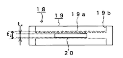
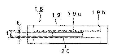
例えば、本発明を、図5に示すように、光学素子としての回折格子18に適用する場合には、回折格子本体19における回折格子形成面に直交する面が側面となり、この側面にゲート部20が形成されることになる。
For example, as shown in FIG. 5, when the present invention is applied to a
なお、図5における回折格子18は、回折格子本体19が、回折格子が形成された光学機能部19aと、この光学機能部19aを囲む筒状の枠部19bとが一体成形されることによって形成されている。
The
この場合であっても、回折格子本体19の光学機能部19aの厚みt3に対するゲート部20の厚みt4の割合および回折格子本体19の光学機能部19aの厚み方向の断面積に対するゲート部20の厚み方向の断面積の割合の少なくとも一方を50%以上に形成することによって、レンズ1の場合と同様に、樹脂材料の転写不良を簡便かつ確実に抑制することができ、光学性能に優れた回折格子18を、歩留まりを向上させつつ安価に製造することができるといった優れた効果を奏することができる。
Even this case, the
また、本発明は、図6に示すように、レンズ本体21の光学機能部22の外側に、光軸Lに直交する水平面を有するフランジ部26が一体成形され、さらに、その外側に、光軸L方向に延びる鏡筒部23が一体成形されたレンズ24にも有効に適用することができるものである。この場合にも、レンズ本体21の光学機能部22の厚みt5に対するゲート部25の厚みt6の割合およびレンズ本体21の光学機能部22の厚み方向の断面積に対するゲート部25の厚み方向の断面積の割合の少なくとも一方を50%以上に形成することによって、上述したレンズ1の場合と同様の効果を奏することができる。
Further, in the present invention, as shown in FIG. 6, a flange portion 26 having a horizontal plane perpendicular to the optical axis L is integrally formed outside the
さらに、上述した実施形態においては、レンズ1の成形材料として熱可塑性樹脂を挙げているが、本発明は、光学素子の成形材料として熱硬化性樹脂を用いる場合にも有効に適用することができるものである。
Furthermore, in the above-described embodiment, a thermoplastic resin is cited as the molding material for the
1 レンズ
1a レンズ本体
1b 光学機能部
2 ゲート部
3 ランナ部
4 スプール部
5 レンズ成形品
7 レンズ成型用金型
10 キャビティ
14 ゲート
15 ランナ
16 スプール
DESCRIPTION OF
Claims (15)
光学素子本体の側面にゲート部が形成され、
前記光学素子本体の光学機能部の厚みに対する前記ゲート部の厚みの割合が50%以上に形成されていることを特徴とする光学素子。 In an optical element molded from a resin material,
A gate part is formed on the side surface of the optical element body,
A ratio of the thickness of the gate part to the thickness of the optical function part of the optical element body is formed to be 50% or more.
光学素子本体の側面にゲート部が形成され、
前記光学素子本体の光学機能部の厚み方向の断面積に対する前記ゲート部の厚み方向の断面積の割合が50%以上に形成されていることを特徴とする光学素子。 In an optical element molded from a resin material,
A gate part is formed on the side surface of the optical element body,
A ratio of a cross-sectional area in the thickness direction of the gate portion to a cross-sectional area in the thickness direction of the optical function portion of the optical element body is formed to be 50% or more.
光学素子本体の側面にゲート部が形成され、
前記光学素子本体の光学機能部の厚みに対する前記ゲート部の厚みの割合が50%以上に形成され、かつ、
前記光学素子本体の前記光学機能部の厚み方向の断面積に対する前記ゲート部の厚み方向の断面積の割合が50%以上に形成されていることを特徴とする光学素子。 In an optical element molded from a resin material,
A gate part is formed on the side surface of the optical element body,
The ratio of the thickness of the gate part to the thickness of the optical function part of the optical element body is formed to be 50% or more, and
A ratio of a cross-sectional area in the thickness direction of the gate portion to a cross-sectional area in the thickness direction of the optical function portion of the optical element body is formed to be 50% or more.
前記ゲートが、前記キャビティ内で成形される光学素子本体の側面に対応する位置に形成され、
前記キャビティにおける前記光学素子本体の光学機能部が成形される部位の厚みに対する前記ゲートの厚みの割合が50%以上に形成されていることを特徴とする光学素子成形用金型。 In an optical element molding die having a cavity filled with a resin material and a gate through which the resin material passes when filling the cavity with the resin material,
The gate is formed at a position corresponding to a side surface of the optical element body molded in the cavity;
A mold for molding an optical element, wherein the ratio of the thickness of the gate to the thickness of the portion of the cavity in which the optical function part of the optical element body is molded is 50% or more.
前記ゲートが、前記キャビティ内で成形される光学素子本体の側面に対応する位置に形成され、
前記キャビティにおける前記光学素子本体の光学機能部が成形される部位の厚み方向の断面積に対する前記ゲートの厚み方向の断面積の割合が50%以上に形成されていることを特徴とする光学素子成形用金型。 In an optical element molding die having a cavity filled with a resin material and a gate through which the resin material passes when filling the cavity with the resin material,
The gate is formed at a position corresponding to a side surface of the optical element body molded in the cavity;
The optical element molding characterized in that the ratio of the cross-sectional area in the thickness direction of the gate to the cross-sectional area in the thickness direction of the portion of the cavity where the optical function part of the optical element body is molded is 50% or more. Mold.
前記ゲートが、前記キャビティ内で成形される光学素子本体の側面に対応する位置に形成され、
前記キャビティにおける前記光学素子本体の光学機能部が成形される部位の厚みに対する前記ゲートの厚みの割合が50%以上に形成され、かつ、
前記キャビティにおける前記光学素子本体の光学機能部が成形される部位の厚み方向の断面積に対するゲートの厚み方向の断面積の割合が50%以上に形成されていることを特徴とする光学素子成形用金型。 In an optical element molding die having a cavity filled with a resin material and a gate through which the resin material passes when filling the cavity with the resin material,
The gate is formed at a position corresponding to a side surface of the optical element body molded in the cavity;
The ratio of the thickness of the gate to the thickness of the portion where the optical function part of the optical element body in the cavity is formed is 50% or more, and
The ratio of the cross-sectional area in the thickness direction of the gate to the cross-sectional area in the thickness direction of the portion in the cavity where the optical functional part of the optical element body is molded is formed to be 50% or more. Mold.
前記ゲートを、前記キャビティ内で成形される光学素子本体の側面に対応する位置に形成した状態で、
前記キャビティにおける前記光学素子本体の光学機能部が成形される部位の厚みに対する前記ゲートの厚みの割合を50%以上にして光学素子を製造することを特徴とする光学素子の製造方法。 In the method of manufacturing an optical element in which an optical element is manufactured by resin molding by curing after filling a molten resin material into a cavity through a gate,
In a state where the gate is formed at a position corresponding to the side surface of the optical element body molded in the cavity,
An optical element manufacturing method, wherein an optical element is manufactured by setting a ratio of a thickness of the gate to a thickness of a portion of the cavity in which an optical function part of the optical element body is formed to 50% or more.
前記ゲートを、前記キャビティ内で成形される光学素子本体の側面に対応する位置に形成した状態で、
前記キャビティにおける前記光学素子本体の光学機能部が成形される部位の厚み方向の断面積に対する前記ゲートの厚み方向の断面積の割合を50%以上にして光学素子を製造することを特徴とする光学素子の製造方法。 In the method of manufacturing an optical element in which an optical element is manufactured by resin molding by curing after filling the cavity with a molten resin material through a gate,
In a state where the gate is formed at a position corresponding to the side surface of the optical element body molded in the cavity,
The optical element is manufactured by setting the ratio of the cross-sectional area in the thickness direction of the gate to the cross-sectional area in the thickness direction of the portion of the cavity in which the optical function part of the optical element body is formed in the thickness direction is 50% or more. Device manufacturing method.
前記ゲートを、前記キャビティ内で成形される光学素子本体の側面に対応する位置に形成した状態で、
前記キャビティにおける前記光学素子本体の光学機能部が成形される部位の厚みに対する前記ゲートの厚みの割合を50%以上にするとともに、前記キャビティにおける前記光学素子本体の光学機能部が成形される部位の厚み方向の断面積に対する前記ゲートの厚み方向の断面積の割合を50%以上にして光学素子を製造することを特徴とする光学素子の製造方法。 In the method of manufacturing an optical element in which an optical element is manufactured by resin molding by curing after filling the cavity with a molten resin material through a gate,
In a state where the gate is formed at a position corresponding to the side surface of the optical element body molded in the cavity,
The ratio of the thickness of the gate to the thickness of the part where the optical function part of the optical element body in the cavity is formed is 50% or more, and the part of the optical function part of the optical element body in the cavity is formed. An optical element manufacturing method, wherein an optical element is manufactured by setting a ratio of a cross-sectional area in the thickness direction of the gate to a cross-sectional area in the thickness direction to 50% or more.
Priority Applications (3)
| Application Number | Priority Date | Filing Date | Title |
|---|---|---|---|
| JP2004348660A JP2006150902A (en) | 2004-12-01 | 2004-12-01 | Optical element, optical element molding die and manufacturing method of optical element |
| US11/285,099 US7525742B2 (en) | 2004-12-01 | 2005-11-21 | Optical element, optical element molding die, and optical element manufacturing method |
| US12/380,625 US7854879B2 (en) | 2004-12-01 | 2009-03-02 | Optical element molding die, and optical element manufacturing method |
Applications Claiming Priority (1)
| Application Number | Priority Date | Filing Date | Title |
|---|---|---|---|
| JP2004348660A JP2006150902A (en) | 2004-12-01 | 2004-12-01 | Optical element, optical element molding die and manufacturing method of optical element |
Publications (1)
| Publication Number | Publication Date |
|---|---|
| JP2006150902A true JP2006150902A (en) | 2006-06-15 |
Family
ID=36583373
Family Applications (1)
| Application Number | Title | Priority Date | Filing Date |
|---|---|---|---|
| JP2004348660A Pending JP2006150902A (en) | 2004-12-01 | 2004-12-01 | Optical element, optical element molding die and manufacturing method of optical element |
Country Status (2)
| Country | Link |
|---|---|
| US (2) | US7525742B2 (en) |
| JP (1) | JP2006150902A (en) |
Cited By (3)
| Publication number | Priority date | Publication date | Assignee | Title |
|---|---|---|---|---|
| WO2011040148A1 (en) * | 2009-09-30 | 2011-04-07 | コニカミノルタオプト株式会社 | Optical element |
| WO2019039049A1 (en) * | 2017-08-24 | 2019-02-28 | 住友電気工業株式会社 | Method for manufacturing optical communication component and optical communication component |
| CN110733165A (en) * | 2018-07-19 | 2020-01-31 | 株式会社小糸制作所 | Mold and resin component |
Families Citing this family (2)
| Publication number | Priority date | Publication date | Assignee | Title |
|---|---|---|---|---|
| JP2013095034A (en) * | 2011-10-31 | 2013-05-20 | Sanyo Electric Co Ltd | Method of manufacturing lens, the lens, and optical device |
| KR101822565B1 (en) * | 2016-02-26 | 2018-01-26 | 서울과학기술대학교 산학협력단 | Injection molded lens using hot runner |
Citations (3)
| Publication number | Priority date | Publication date | Assignee | Title |
|---|---|---|---|---|
| JPH02270524A (en) * | 1989-04-13 | 1990-11-05 | Hitachi Ltd | plastic lens mold |
| JPH03211030A (en) * | 1990-01-17 | 1991-09-13 | Hitachi Ltd | Plastic lens |
| JP2003245946A (en) * | 2002-02-25 | 2003-09-02 | Matsushita Electric Ind Co Ltd | Optical element, optical element molding die and optical element molding method |
Family Cites Families (4)
| Publication number | Priority date | Publication date | Assignee | Title |
|---|---|---|---|---|
| JP3130099B2 (en) | 1991-12-27 | 2001-01-31 | 株式会社リコー | Manufacturing method of plastic molded products |
| JPH08271703A (en) * | 1995-03-29 | 1996-10-18 | Konica Corp | Resin lens |
| JPH1111561A (en) * | 1997-06-24 | 1999-01-19 | Fuji Photo Optical Co Ltd | Lens case |
| WO2006046437A1 (en) * | 2004-10-29 | 2006-05-04 | Konica Minolta Opto, Inc. | Optical component production system |
-
2004
- 2004-12-01 JP JP2004348660A patent/JP2006150902A/en active Pending
-
2005
- 2005-11-21 US US11/285,099 patent/US7525742B2/en not_active Expired - Fee Related
-
2009
- 2009-03-02 US US12/380,625 patent/US7854879B2/en not_active Expired - Fee Related
Patent Citations (3)
| Publication number | Priority date | Publication date | Assignee | Title |
|---|---|---|---|---|
| JPH02270524A (en) * | 1989-04-13 | 1990-11-05 | Hitachi Ltd | plastic lens mold |
| JPH03211030A (en) * | 1990-01-17 | 1991-09-13 | Hitachi Ltd | Plastic lens |
| JP2003245946A (en) * | 2002-02-25 | 2003-09-02 | Matsushita Electric Ind Co Ltd | Optical element, optical element molding die and optical element molding method |
Cited By (3)
| Publication number | Priority date | Publication date | Assignee | Title |
|---|---|---|---|---|
| WO2011040148A1 (en) * | 2009-09-30 | 2011-04-07 | コニカミノルタオプト株式会社 | Optical element |
| WO2019039049A1 (en) * | 2017-08-24 | 2019-02-28 | 住友電気工業株式会社 | Method for manufacturing optical communication component and optical communication component |
| CN110733165A (en) * | 2018-07-19 | 2020-01-31 | 株式会社小糸制作所 | Mold and resin component |
Also Published As
| Publication number | Publication date |
|---|---|
| US7525742B2 (en) | 2009-04-28 |
| US7854879B2 (en) | 2010-12-21 |
| US20060126014A1 (en) | 2006-06-15 |
| US20090230581A1 (en) | 2009-09-17 |
Similar Documents
| Publication | Publication Date | Title |
|---|---|---|
| KR101821859B1 (en) | Molding tool and method for the production of an optical element | |
| CN106166822B (en) | Optical component molding method, molding device, and optical component | |
| EP2266776A1 (en) | Method and device for producing thick-walled plastic components, in particular optical components | |
| KR101243401B1 (en) | Optical component production system and method for producing the same | |
| US7854879B2 (en) | Optical element molding die, and optical element manufacturing method | |
| JP2009037162A5 (en) | ||
| KR101673207B1 (en) | Gate cutting block and gate cutting device for mold product | |
| KR101271772B1 (en) | Optical component production system | |
| JPWO2012043190A1 (en) | Lens manufacturing method | |
| CN101585226B (en) | Lens forming die and forming method thereof | |
| JP4658651B2 (en) | Injection molded body, injection molding body manufacturing method and manufacturing apparatus | |
| JP4097954B2 (en) | Optical element, optical element molding die, and optical element molding method | |
| WO2011069792A1 (en) | Method and device for producing optical components | |
| AU2002239904B8 (en) | Method for fabricating a plastic optic element injection mold | |
| JP2008257261A (en) | Optical element, optical element molding die, and optical element molding method | |
| JP2010210818A (en) | Method for manufacturing optical component | |
| KR101655335B1 (en) | Injection molded lens | |
| JP6765840B2 (en) | Manufacturing methods for plastic lenses, optics, and plastic lenses | |
| JP5963522B2 (en) | Parts manufacturing method | |
| JP4883331B2 (en) | Optical element manufacturing method for optical pickup apparatus and optical element manufacturing apparatus for optical pickup apparatus | |
| JP6245930B2 (en) | Manufacturing method of plastic optical member | |
| JP2008284704A (en) | Mold and method of manufacturing optical element | |
| JP2008077064A (en) | Prism and prism coupling object | |
| JP6179522B2 (en) | Mold, optical element manufacturing method, and optical element | |
| JP2017217850A (en) | Method for molding thick-walled molded article |
Legal Events
| Date | Code | Title | Description |
|---|---|---|---|
| A621 | Written request for application examination |
Free format text: JAPANESE INTERMEDIATE CODE: A621 Effective date: 20071113 |
|
| A977 | Report on retrieval |
Free format text: JAPANESE INTERMEDIATE CODE: A971007 Effective date: 20100527 |
|
| A131 | Notification of reasons for refusal |
Free format text: JAPANESE INTERMEDIATE CODE: A131 Effective date: 20100601 |
|
| A521 | Written amendment |
Free format text: JAPANESE INTERMEDIATE CODE: A523 Effective date: 20100729 |
|
| A02 | Decision of refusal |
Free format text: JAPANESE INTERMEDIATE CODE: A02 Effective date: 20110426 |