JP2006172702A - Column selection line signal generation device for semiconductor memory device - Google Patents
Column selection line signal generation device for semiconductor memory device Download PDFInfo
- Publication number
- JP2006172702A JP2006172702A JP2005359515A JP2005359515A JP2006172702A JP 2006172702 A JP2006172702 A JP 2006172702A JP 2005359515 A JP2005359515 A JP 2005359515A JP 2005359515 A JP2005359515 A JP 2005359515A JP 2006172702 A JP2006172702 A JP 2006172702A
- Authority
- JP
- Japan
- Prior art keywords
- selection line
- column selection
- command
- signal
- clock cycle
- Prior art date
- Legal status (The legal status is an assumption and is not a legal conclusion. Google has not performed a legal analysis and makes no representation as to the accuracy of the status listed.)
- Granted
Links
Images




Classifications
-
- G—PHYSICS
- G11—INFORMATION STORAGE
- G11C—STATIC STORES
- G11C8/00—Arrangements for selecting an address in a digital store
- G11C8/10—Decoders
-
- G—PHYSICS
- G11—INFORMATION STORAGE
- G11C—STATIC STORES
- G11C7/00—Arrangements for writing information into, or reading information out from, a digital store
- G11C7/10—Input/output [I/O] data interface arrangements, e.g. I/O data control circuits, I/O data buffers
- G11C7/1048—Data bus control circuits, e.g. precharging, presetting, equalising
-
- G—PHYSICS
- G11—INFORMATION STORAGE
- G11C—STATIC STORES
- G11C7/00—Arrangements for writing information into, or reading information out from, a digital store
-
- G—PHYSICS
- G11—INFORMATION STORAGE
- G11C—STATIC STORES
- G11C7/00—Arrangements for writing information into, or reading information out from, a digital store
- G11C7/10—Input/output [I/O] data interface arrangements, e.g. I/O data control circuits, I/O data buffers
- G11C7/1006—Data managing, e.g. manipulating data before writing or reading out, data bus switches or control circuits therefor
- G11C7/1012—Data reordering during input/output, e.g. crossbars, layers of multiplexers, shifting or rotating
-
- G—PHYSICS
- G11—INFORMATION STORAGE
- G11C—STATIC STORES
- G11C7/00—Arrangements for writing information into, or reading information out from, a digital store
- G11C7/10—Input/output [I/O] data interface arrangements, e.g. I/O data control circuits, I/O data buffers
- G11C7/1051—Data output circuits, e.g. read-out amplifiers, data output buffers, data output registers, data output level conversion circuits
-
- G—PHYSICS
- G11—INFORMATION STORAGE
- G11C—STATIC STORES
- G11C7/00—Arrangements for writing information into, or reading information out from, a digital store
- G11C7/10—Input/output [I/O] data interface arrangements, e.g. I/O data control circuits, I/O data buffers
- G11C7/1051—Data output circuits, e.g. read-out amplifiers, data output buffers, data output registers, data output level conversion circuits
- G11C7/1066—Output synchronization
-
- G—PHYSICS
- G11—INFORMATION STORAGE
- G11C—STATIC STORES
- G11C7/00—Arrangements for writing information into, or reading information out from, a digital store
- G11C7/10—Input/output [I/O] data interface arrangements, e.g. I/O data control circuits, I/O data buffers
- G11C7/1051—Data output circuits, e.g. read-out amplifiers, data output buffers, data output registers, data output level conversion circuits
- G11C7/1069—I/O lines read out arrangements
-
- G—PHYSICS
- G11—INFORMATION STORAGE
- G11C—STATIC STORES
- G11C7/00—Arrangements for writing information into, or reading information out from, a digital store
- G11C7/22—Read-write [R-W] timing or clocking circuits; Read-write [R-W] control signal generators or management
-
- G—PHYSICS
- G11—INFORMATION STORAGE
- G11C—STATIC STORES
- G11C2207/00—Indexing scheme relating to arrangements for writing information into, or reading information out from, a digital store
- G11C2207/002—Isolation gates, i.e. gates coupling bit lines to the sense amplifier
Landscapes
- Engineering & Computer Science (AREA)
- Microelectronics & Electronic Packaging (AREA)
- Dram (AREA)
- Static Random-Access Memory (AREA)
Abstract
【課題】 半導体メモリ装置のカラム選択線信号生成装置を提供することにある。
【解決手段】 半導体メモリ装置のカラム選択線信号生成装置において、コマンドがライト命令に連続して印加される場合には第1動作モードを有し、前記コマンドが前記ライト命令に連続して印加されない場合には第2動作モードを有し、カラム選択線イネーブル信号によりカラム選択線信号がイネーブルされ、前記カラム選択線信号の動作区間は前記第1及び第2動作モードで互いに異なることを特徴とする。
【選択図】 図2PROBLEM TO BE SOLVED: To provide a column selection line signal generation device of a semiconductor memory device.
In a column selection line signal generation device of a semiconductor memory device, a command has a first operation mode when a command is applied continuously to a write command, and the command is not applied continuously to the write command. In some cases, the column selection line signal is enabled by a column selection line enable signal, and the operation period of the column selection line signal is different between the first and second operation modes. .
[Selection] Figure 2
Description
本発明は、半導体メモリ装置に係るもので、詳しくは、半導体メモリ装置のカラム選択線信号生成装置に関する。 The present invention relates to a semiconductor memory device, and more particularly, to a column selection line signal generation device for a semiconductor memory device.
半導体メモリ装置の動作特性を表す要素の中にtRDLというアクティブ・コマンドパラメーターがある。tRDLは時間的な面からみたときにカラム選択線信号(CSL)のサイクル数と密接に関連する。即ち、カラム選択線信号の以前のいくつかのサイクルの間に継続的にデータをライトする途中で、進行しているライト動作がロープリチャージ命令によりインターラプトされたとき、最後のデータが完全にライトされ、且つロープリチャージ命令が入力されるためには最低でもtRDL区間が存在すべきであることを示す。 An active command parameter called tRDL is one of the elements representing the operating characteristics of the semiconductor memory device. tRDL is closely related to the number of cycles of the column select line signal (CSL) when viewed from a temporal aspect. That is, when the ongoing write operation is interrupted by a row precharge command in the middle of continuously writing data during several previous cycles of the column select line signal, the last data is completely written. And at least a tRDL period should exist for the low precharge command to be input.
図6はtRDLを説明するためのタイミング図である。 FIG. 6 is a timing chart for explaining tRDL.
図6を参照すると、tRDLはライト命令によりデータDb0,Db1,Db2,Db3のうち最後のデータDb3がビットラインに印加されてからロープリチャージ命令RPCが印加される時点までの時間である。 Referring to FIG. 6, tRDL is a time from when the last data Db3 of the data Db0, Db1, Db2, and Db3 is applied to the bit line by the write command to when the low precharge command RPC is applied.
図7は従来の半導体メモリ装置でのカラム選択経路を示すブロック図である。 FIG. 7 is a block diagram showing a column selection path in a conventional semiconductor memory device.
図7を参照すると、コマンドバッファ22、カラム選択線イネーブル部24、カラム選択線ディスエーブル部25、カラム選択線ドライバ26、PDT発生器27、IOドライバ/MUX28、ビットラインセンスアンプ29、及びメモリセルMCが図示される。
Referring to FIG. 7, a command buffer 22, a column selection line enable
コマンドバッファ22はコマンドCMDが動作クロックCLKに応ずるようにして動作活性化信号PWAXまたはPCAを出力する。 The command buffer 22 outputs the operation activation signal PWAX or PCA so that the command CMD responds to the operation clock CLK.
カラム選択線イネーブル部24は動作活性化信号PWAXまたはPCAを受信してカラム選択線イネーブル信号PCSLEを出力する。
The column selection line enable
カラム選択線ディスエーブル部25は動作活性化信号PWAXまたはPCAを受信した後、動作クロックサイクルの次の動作クロックサイクルに応じてカラム選択線ディスエーブル信号PCSLDを生成する。 After receiving the operation activation signal PWAX or PCA, the column selection line disable unit 25 generates the column selection line disable signal PCSLD according to the operation clock cycle next to the operation clock cycle.
カラム選択線ドライバ26はカラム選択線イネーブル信号PCSLE及びカラム選択線ディスエーブル信号PCSLDの制御を受けてカラム選択線信号CSLを出力する。 The column selection line driver 26 outputs a column selection line signal CSL under the control of the column selection line enable signal PCSLE and the column selection line disable signal PCSLD.
PDT発生器27はカラム選択線信号CSLを受信してIOドライバ/MUX28のイネーブル信号PDTを出力する。
The PDT generator 27 receives the column selection line signal CSL and outputs an enable signal PDT for the IO driver /
ライトされるデータは、カラム選択線信号CSLがハイ状態にある場合にはトランジスタTR1がオン状態となり、IOドライバ/MUX28もPDT信号によりイネーブルされて、ビットラインセンスアンプ29によりセンシングされビットラインBL/BLBに印加される。そして、前記データは最終的にメモリセルMCにライトされる。
When the column selection line signal CSL is in a high state, the transistor TR1 is turned on, and the IO driver /
図8は図7のカラム選択線信号CSLが生成される過程を示すタイミング図である。 FIG. 8 is a timing diagram illustrating a process of generating the column selection line signal CSL of FIG.
図8を参照すると、動作クロックCLK、コマンドWR1,WR2,RD、動作活性化信号PWAX,PCA、カラム選択線イネーブル信号PCSLE、カラム選択線ディスエーブル信号PCSLD、及びカラム選択線信号CSLが図示される。コマンドは図7でのCMDであり、図8では具体的な動作のライトWR1,WR2またはリードRDとして示す。 Referring to FIG. 8, an operation clock CLK, commands WR1, WR2, and RD, operation activation signals PWAX and PCA, a column selection line enable signal PCSLE, a column selection line disable signal PCSLD, and a column selection line signal CSL are illustrated. . The command is CMD in FIG. 7, and in FIG. 8, it is shown as write WR1, WR2 or read RD of a specific operation.
まず、ライト命令WR1が印加され、動作クロックCLKでの動作クロックサイクルに応じてライト活性化信号PWAXが生成される。 First, the write command WR1 is applied, and the write activation signal PWAX is generated according to the operation clock cycle of the operation clock CLK.
ライト活性化信号PWAXに応じてカラム選択線イネーブル信号PCSLEが生成され、カラム選択線イネーブル信号PCSLEによりカラム選択線信号CSLが活性化される。 A column selection line enable signal PCSLE is generated in response to the write activation signal PWAX, and the column selection line signal CSL is activated by the column selection line enable signal PCSLE.
動作クロックサイクルよりも1動作クロックサイクル以後の第2動作クロックサイクルに応じてカラム選択線ディスエーブル信号PCSLDが生成され、カラム選択線ディスエーブル信号PCSLDによりカラム選択線信号CSLが非活性化される。 The column selection line disable signal PCSLD is generated according to the second operation clock cycle after one operation clock cycle from the operation clock cycle, and the column selection line signal CSL is deactivated by the column selection line disable signal PCSLD.
次いで、ライト命令WR2が印加された後、ライト命令WR1が応ずる動作クロックサイクルよりも2動作サイクル以後の第3動作クロックサイクルに応じてライト活性化信号PWAXが生成されて、ライト命令WR1が印加された場合と同一な過程によりカラム選択線信号CSLが生成される。 Next, after the write command WR2 is applied, the write activation signal PWAX is generated according to the third operation clock cycle after the second operation cycle rather than the operation clock cycle to which the write command WR1 responds, and the write command WR1 is applied. The column selection line signal CSL is generated by the same process as that described above.
第3動作クロックサイクル以後の動作クロックサイクルに応じてリード活性化信号PCAが生成される場合、リード活性化信号PCAに応じてカラム選択線イネーブル信号PCSLEが生成される。そして、カラム選択線イネーブル信号PCSLEに応じてカラム選択線信号CSLが活性化される。 When the read activation signal PCA is generated according to the operation clock cycle after the third operation clock cycle, the column selection line enable signal PCSLE is generated according to the read activation signal PCA. Then, the column selection line signal CSL is activated in response to the column selection line enable signal PCSLE.
第3動作クロックサイクル以後の動作クロックサイクルよりも1動作クロックサイクル以後の動作クロックサイクルに応じてカラム選択線ディスエーブル信号PCSLDが生成され、カラム選択線ディスエーブル信号PCSLDによりカラム選択線信号CSLは非活性化される。 The column selection line disable signal PCSLD is generated according to the operation clock cycle after one operation clock cycle rather than the operation clock cycle after the third operation clock cycle. The column selection line disable signal PCSLD causes the column selection line signal CSL to be non- Activated.
リード活性化信号PCAの代わりにライト活性化信号PWAXが生成される場合、即ち、リード命令RDの代わりにライト命令が印加される場合にはカラム選択線イネーブル信号の生成がライト活性化信号PWAXに応じて生成されることを除き、カラム選択線信号CSLは同一な過程により活性化され非活性化される。 When the write activation signal PWAX is generated instead of the read activation signal PCA, that is, when the write command is applied instead of the read command RD, the generation of the column selection line enable signal is changed to the write activation signal PWAX. Except being generated accordingly, the column select line signal CSL is activated and deactivated by the same process.
上述のように、カラム選択線信号はカラム選択線イネーブル信号に応じて活性化され、カラム選択線イネーブル信号が生成される動作クロックサイクルよりも1動作クロックサイクル後の第2動作クロックサイクルに応じて生成されたカラム選択線ディスエーブル信号により非活性化される形態の単一動作モードだけを有する。 As described above, the column selection line signal is activated according to the column selection line enable signal, and according to the second operation clock cycle one operation clock cycle after the operation clock cycle in which the column selection line enable signal is generated. It has only a single operation mode in a form deactivated by the generated column select line disable signal.
ところが、ライト命令以後にビットラインプリチャージが行われる場合において、メモリセルにライトされるデータ中で最後のデータがビットラインに印加された後、メモリセルに完全にライトされる以前にメモリセルのワードラインがディスエーブルされて、メモリセルに最後のデータが正しくライトされないとの問題点があった。これはビットラインセンスアンプの駆動能力がIOドライバのそれよりも劣るからである。従って、駆動能力が優秀なIOドライバによる駆動時間を一層増加させなければならない。 However, when bit line precharge is performed after the write command, the last data in the data written to the memory cell is applied to the bit line and then completely written to the memory cell. There is a problem in that the last data is not correctly written to the memory cell because the word line is disabled. This is because the driving capability of the bit line sense amplifier is inferior to that of the IO driver. Therefore, it is necessary to further increase the driving time by an IO driver having excellent driving capability.
そこで、本発明の目的は、カラム選択線信号がコマンドの印加形態に従い互いに異なった形態の動作モードを有することができるカラム選択線信号生成装置及び方法を提供することにある。 SUMMARY OF THE INVENTION Accordingly, an object of the present invention is to provide a column selection line signal generation apparatus and method in which column selection line signals can have different operation modes according to command application modes.
本発明の他の目的は、従来のメモリセルに完全にライトされる以前にビットラインのプリチャージが行われることにより、メモリセルに最後のデータが正しくライトされないとの問題を改善することができるカラム選択線信号生成装置及び方法を提供することにある。 Another object of the present invention is to improve the problem that the last data is not correctly written in the memory cell by precharging the bit line before it is completely written in the conventional memory cell. An object of the present invention is to provide a column selection line signal generation apparatus and method.
本発明のまた他の目的は、プリチャージ以前のライト動作整理時間tRDLは速くすることにより、プリチャージ前のライト動作整理時間のマージンが広くなってメモリセルにライトされるデータの損失を減らし得るカラム選択線信号生成装置及び方法を提供することにある。 Another object of the present invention is to shorten the write operation arrangement time tRDL before precharge, thereby widening the margin of the write operation arrangement time before precharge and reducing the loss of data written to the memory cell. An object of the present invention is to provide a column selection line signal generation apparatus and method.
本発明のまた他の目的は、コマンドがライト命令に連続して印加される場合にカラム選択線信号の幅を広くして、IOドライバの駆動時間を長くし、メモリセルにデータライトが速く行われるようにして、ロープリチャージ時点を速くすることができるカラム選択線信号生成装置及び方法を提供することにある。 Another object of the present invention is to increase the width of the column selection line signal and extend the driving time of the IO driver when the command is continuously applied to the write command, and to perform the data write to the memory cell faster. Thus, it is an object of the present invention to provide a column selection line signal generation apparatus and method capable of speeding up the row precharge time.
本発明のまた他の目的は、ロープリチャージ時点を速くすることにより、高速動作を可能にするカラム選択回路を備えた半導体メモリ装置を提供することにある。 Another object of the present invention is to provide a semiconductor memory device including a column selection circuit that enables high-speed operation by increasing the time of row precharge.
このような目的を達成するために本発明の好適な一実施形態による半導体メモリ装置のカラム選択線信号生成装置は、コマンドがライト命令に連続して印加される場合には第1動作モードを有し、前記コマンドが前記ライト命令に連続して印加されない場合には第2動作モードを有し、イネーブル信号が入力された場合には第1,2区間制御信号に応じて前記第1,2動作モードで互いに異なったパルス区間を有するカラム選択線信号を生成するカラム選択線信号生成部と、前記第1動作モードではコマンド活性化信号により前記第1区間制御信号を出力し、前記第2動作モードではカラム選択線ディスエーブル信号により前記第1区間制御信号の遷移時点とは異なった前記第2区間制御信号を出力する区間制御信号生成部と、を備えることを特徴とする。 In order to achieve such an object, a column selection line signal generation device of a semiconductor memory device according to a preferred embodiment of the present invention has a first operation mode when a command is continuously applied to a write command. When the command is not continuously applied to the write command, the second operation mode is provided. When the enable signal is input, the first and second operations are performed according to the first and second section control signals. A column selection line signal generator for generating column selection line signals having different pulse intervals in each mode; and, in the first operation mode, outputting the first interval control signal by a command activation signal, and the second operation mode A section control signal generation unit that outputs the second section control signal different from the transition point of the first section control signal by a column selection line disable signal. And it features.
ここで、前記イネーブル信号は動作クロックサイクルに応じて印加された前記コマンドにより生成された動作活性化信号に応じて生成されることができる。 Here, the enable signal may be generated according to an operation activation signal generated by the command applied according to an operation clock cycle.
また、前記第1区間制御信号の遷移時点は前記第2区間遷移時点よりも早いことが好ましい。 In addition, it is preferable that the transition time of the first section control signal is earlier than the second section transition time.
また、前記第1区間制御信号は前記コマンドに応じて遷移されることが好ましい。 Further, it is preferable that the first section control signal is transitioned according to the command.
また、前記第2区間制御信号は前記動作クロックサイクルの次の動作クロックサイクルの第2動作クロックサイクルにより生成されたディスエーブル信号に応じて遷移されることが好ましい。 The second interval control signal may be transitioned according to a disable signal generated by a second operation clock cycle of the operation clock cycle subsequent to the operation clock cycle.
また、前記コマンドは前記第1動作モードで前記第2動作クロックサイクルの次の動作クロックサイクルの第3動作クロックサイクルに応じて印加されることが好ましい。 The command may be applied according to a third operation clock cycle of an operation clock cycle subsequent to the second operation clock cycle in the first operation mode.
また、前記コマンドは前記第2動作モードで前記第3動作クロックサイクル後の第4動作クロックサイクルに応じて印加されることが好ましい。 The command may be applied according to a fourth operation clock cycle after the third operation clock cycle in the second operation mode.
本発明の好適な他の実施形態による半導体メモリ装置のカラム選択線信号生成装置は、コマンドがライト命令に連続して印加される場合には第1動作モードを有し、前記コマンドが前記ライト命令に連続して印加されない場合には第2動作モードを有し、前記コマンドにより生成されるイネーブル信号が入力された場合に第1,2区間制御信号に応じて前記第1,2動作モードで互いに異なったパルス区間を有するカラム選択線信号を生成するカラム選択線信号生成部と、前記第1動作モードでは前記コマンドが印加される動作クロックサイクルの次の動作クロックサイクルと遷移時点が略一致するプリコマンドパルスに応じて前記第1区間制御信号を出力し、前記第2動作モードではディスエーブル信号に応じて前記第2区間制御信号を前記第1区間制御信号の遷移時点とは異なるように出力する区間制御信号生成部と、を備える。 A column selection line signal generation device of a semiconductor memory device according to another embodiment of the present invention has a first operation mode when a command is continuously applied to a write command, and the command is the write command. In the first and second operation modes according to the first and second section control signals when the enable signal generated by the command is input. A column selection line signal generation unit for generating a column selection line signal having a different pulse period; The first interval control signal is output in response to a command pulse, and the second interval control signal is output in advance in the second operation mode in response to a disable signal. And a period control signal generator outputting differently than the transition point of the first interval control signal.
ここで、前記プリコマンドパルスは前記第1動作モードで前記ディスエーブル信号に先立って生成されることが好ましい。 The pre-command pulse may be generated prior to the disable signal in the first operation mode.
また、前記プリコマンドパルスは前記第2動作モードで前記ディスエーブル信号よりも遅く生成されることが好ましい。 The precommand pulse may be generated later than the disable signal in the second operation mode.
また、前記第1区間制御信号の遷移時点は前記第2区間遷移時点よりも早いことが好ましい。 In addition, it is preferable that the transition time of the first section control signal is earlier than the second section transition time.
本発明の好適な更に他の実施形態による半導体メモリ装置は、一つのアクセストランジスタとストレージキャパシタからなる単位メモリセルが行と列の交差点にマトリックス形態に連結されたメモリブロックを複数として有するメモリセルアレイと、前記メモリセルの行を選択するためのロー選択回路と、コマンドがライト命令に連続して印加される場合には第1動作モードを有し、前記コマンドが前記ライト命令に連続して印加されない場合には第2動作モードを有し、イネーブル信号が入力される場合には第1,2区間制御信号に応じて前記第1,2動作モードで互いに異なったパルス区間を有するカラム選択線信号を生成するカラム選択線信号生成部と、前記第1動作モードでは前記第1区間制御信号を出力し、前記第2動作モードでは前記第1区間制御信号の遷移時点とは異なった前記第2区間制御信号を出力する区間制御信号生成部と、を備えて、前記メモリセルの列を選択するためのカラム選択回路を有することを特徴とする。 According to still another preferred embodiment of the present invention, a semiconductor memory device includes a memory cell array having a plurality of memory blocks in which unit memory cells each composed of one access transistor and a storage capacitor are connected in a matrix form at intersections of rows and columns; A row selection circuit for selecting a row of the memory cells, and a first operation mode when a command is continuously applied to a write command, and the command is not applied continuously to the write command. If the enable signal is input, the column selection line signal having different pulse sections in the first and second operation modes according to the first and second section control signals is received. A column selection line signal generation unit that generates the first section control signal in the first operation mode, and the second operation mode; A section control signal generator for outputting the second section control signal different from the transition time of the first section control signal, and a column selection circuit for selecting a column of the memory cells. Features.
ここで、前記区間制御信号生成部は、前記第1動作モードではコマンド活性化信号により第1区間制御信号を出力し、第2動作モードではカラム選択線ディスエーブル信号により第2区間制御信号を出力することが好ましい。 The section control signal generator outputs a first section control signal using a command activation signal in the first operation mode, and outputs a second section control signal using a column selection line disable signal in the second operation mode. It is preferable to do.
本発明の好適な更に他の実施形態に従い、データアクセスのためにメモリセルと連結されるカラムラインを選択するためにカラム選択線信号を用いる半導体メモリ装置でのカラム線選択信号生成回路は、前記データアクセスのためのコマンドが設定された連続ウィンド区間内でライト命令に連続して印加されるかどうかをチェックする連続判定部と、前記連続判定部に動作的に連結され、連続されるかどうかに従い互いに異なったパルス区間を有するカラム選択線信号を差別的に生成する信号生成部と、を備えることを特徴とする。 According to still another preferred embodiment of the present invention, a column line selection signal generation circuit in a semiconductor memory device using a column selection line signal to select a column line connected to a memory cell for data access includes: A continuous determination unit that checks whether a command for data access is continuously applied to a write command within a set continuous window section, and whether the command is continuously connected to the continuous determination unit. And a signal generation unit that differentially generates column selection line signals having different pulse sections.
ここで、前記連続ウィンド区間は前記コマンドが応答する動作クロックサイクルから、該動作クロックサイクルよりも2サイクル以前の動作クロックサイクルに応じてライト命令が入力される区間であることが好ましい。 Here, it is preferable that the continuous window period is an area in which a write command is input in accordance with an operation clock cycle two cycles before the operation clock cycle from an operation clock cycle to which the command responds.
このような目的を達成するために本発明の好適な更に他の実施形態により、データアクセスのためにメモリセルと連結されるカラムラインを選択するカラム選択回路を備えた半導体メモリ装置でのカラム選択線信号生成方法は、前記データアクセスのためのコマンドが設定された連続ウィンド区間内でライト命令に連続して印加されるかどうかに従い、互いに異なったパルス区間を有するカラム選択線信号を差別的に生成することを特徴とする。 In order to achieve the above object, a column selection in a semiconductor memory device having a column selection circuit for selecting a column line connected to a memory cell for data access according to still another preferred embodiment of the present invention. The line signal generation method discriminates column selection line signals having different pulse intervals according to whether the command for data access is continuously applied to a write command within a continuous window interval in which the command is set. It is characterized by generating.
本発明は、改善されたカラム選択線信号生成装置を提供することにより、カラム選択線信号がコマンドの印加形態に従い互いに異なった形態の動作モードを有するという効果がある。 The present invention provides an improved column selection line signal generation apparatus, and thus has an effect that the column selection line signals have different modes of operation according to the application mode of the command.
また、本発明は、カラム選択線信号生成装置は改善されたカラム選択線信号発生装置を提供することにより、最後のデータがメモリセルにライトされる前に前記ビットラインのプリチャージが行われる問題を減少させて前記メモリセルに最後のデータまで損傷されずにライトされることができるとの効果がある。 In addition, the present invention provides a column selection line signal generator having an improved column selection line signal generator, whereby the bit line is precharged before the last data is written to the memory cell. Thus, the memory cell can be written without damaging the last data.
また、本発明は、改善されたカラム選択信号生成装置を提供することにより、プリチャージ前のライト動作整理時間tRDLを速く持ってくるようにし、前記プリチャージ前ライト動作整理時間のマージンが広くなってメモリセルにライトされるデータの損失を減らし得るとの効果がある。 In addition, the present invention provides an improved column selection signal generation device so that the write operation arrangement time tRDL before precharge is quickly brought, and the margin of the write operation arrangement time before precharge is widened. Thus, the loss of data written to the memory cell can be reduced.
また、本発明は、改善されたカラム選択信号生成装置を提供して、コマンドがライト命令に連続して印加される場合にカラム選択線信号の幅を広くし且つメモリセルにデータライトが速く行われるすることにより、ロープリチャージ時点を速くし、半導体メモリ装置の高速動作を可能にするとの効果がある。 In addition, the present invention provides an improved column selection signal generating device, which widens the column selection line signal when a command is continuously applied to a write command and performs data write to a memory cell quickly. As a result, there is an effect that the time point of the row precharge is made faster and the semiconductor memory device can be operated at high speed.
以下、本発明の好ましい実施形態を添付図を用いて詳しく説明する。多様な実施形態での説明は当業者に本発明の徹底した理解を助けるための意図のほか、別の意図なしに例示的に図示され限定されたものにすぎないため、本発明の範囲を制限するものとして使用されてはならない。 Hereinafter, preferred embodiments of the present invention will be described in detail with reference to the accompanying drawings. The description in the various embodiments is intended to help those skilled in the art to have a thorough understanding of the present invention, and is intended to limit the scope of the present invention only by way of illustration and limitation without any other intention. Must not be used as
図1は本発明の好適な一実施形態による半導体メモリ装置でのカラム選択経路を概略的に示すブロック図である。 FIG. 1 is a block diagram schematically showing a column selection path in a semiconductor memory device according to a preferred embodiment of the present invention.
図1を参照すると、コマンドバッファ122、カラム選択線イネーブル部124、カラム選択線ディスエーブル部125、PDT発生器127、IOドライバ/MUX128、ビットラインセンスアンプ129、メモリセルMC、及びカラム選択線信号生成装置201が図示される。カラム選択信号生成装置201は遅延セル130及び可変カラム選択線ドライバ200を含む。
Referring to FIG. 1, a
コマンドバッファ122はコマンドCMDを受信し、動作クロックCLKに応じて動作活性化信号PWAX,PCAを出力する。
The
カラム選択線イネーブル部124は動作活性化信号PWAX,PCAを受信してカラム選択線イネーブル信号PCSLEを生成する。即ち、カラム選択線イネーブル部124は動作活性化信号PWAX,PCAに応じてカラム選択線イネーブル信号PCSLEを生成する。
The column selection line enable
カラム選択線ディスエーブル部125は動作活性化信号PWAX,PCAを受信し、動作クロックサイクルの次の動作クロックサイクルに応じてカラム選択線ディスエーブル信号PCSLDを生成する。即ち、カラム選択線ディスエーブル部125は動作クロックサイクルの次の動作クロックサイクルの第2動作クロックサイクルに応じてカラム選択線ディスエーブル信号PCSLDを生成する。
The column selection line disable
カラム選択線信号生成装置201における可変カラム選択線ドライバ200は、カラム選択線イネーブル信号PCSLEが入力される場合、第1,2区間制御信号に応じて第1,2動作モードで互いに異なったパルス区間を有するカラム選択線信号CSLを生成する。即ち、カラム選択線信号装置により、コマンドCMDがライト命令に連続して印加される場合には第1動作モードを有し、コマンドCMDがライト命令に連続して印加されない場合には第2動作モードを有するカラム選択線信号CSLを生成する。詳しくは、第1区間制御信号は動作活性化信号(ライトの場合にPWAX1)に応じて遷移され、第1区間制御信号はカラム選択線ディスエーブル信号PCSLDにより遷移される。ここで、カラム選択線信号の活性化は第1,2動作モードの全てにおいて動作活性化信号PWAX1に応じて活性化されたカラム選択線イネーブル信号PCSLEによりなされる。第2動作モードにおいてライト命令後にリード命令が入力された場合、動作活性化信号PCA1に応じて活性化されたカラム選択線イネーブル信号PCSLEによりカラム選択線信号CSLが活性化される。
When the column selection line enable signal PCSLE is input, the variable column
カラム選択線信号生成装置201における遅延セル130は、第2区間制御信号を生成するためにカラム選択線ディスエーブル信号PCSLDを遅延させる。遅延セル(DC)130としては、通常使用される遅延回路(例えば、1つ或いはそれ以上のインバーター回路)を使用することができる。
The
PDT発生器127はカラム選択線信号CSLを受信してIOドライバ/MUX128のイネーブル信号であるPDT信号を出力する。
The PDT generator 127 receives the column selection line signal CSL and outputs a PDT signal that is an enable signal for the IO driver /
ライトされるデータは、カラム選択線信号がハイ状態にある場合にはトランジスタTR10がオン状態となり、IOドライバ/MUX128もPDT信号によりイネーブルされて、データはビットラインBL/BLBに印加される。そして、データは最終的にメモリセルMCにライトされる。
When data is written, the transistor TR10 is turned on when the column selection line signal is in the high state, the IO driver /
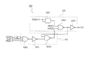
図2は図1のカラム選択線信号生成装置の等価回路図である。 FIG. 2 is an equivalent circuit diagram of the column selection line signal generation device of FIG.
図2を参照すると、カラム選択線信号生成部210及び区間制御信号生成部220が図示される。
Referring to FIG. 2, a column selection
カラム選択線信号生成部210は、コマンドがライト命令に連続して印加される場合には第1動作モードを有し、コマンドがライト命令に連続して印加されない場合には第2動作モードを有するカラム選択線信号を生成する。そして、カラム選択線信号CSLはイネーブル信号であるカラム選択線イネーブル信号PCSLEが入力された場合に第1,2区間制御信号に応じて第1,2動作モードで互いに異なったパルス区間を有する。
The column selection line
区間制御信号生成部220は第1動作モードでは動作活性化信号PWAX1に応じて第1区間制御信号を出力し、第2動作モードではカラム選択線ディスエーブル信号PCSLDに応じて第1区間制御信号の遷移時点とは異なった第2区間制御信号を出力する。
The section
データアクセスのためにコマンドCMDが設定された連続ウィンド区間内でライト命令WR1,WR2に連続的に印加されるかどうかをチェックする連続判定部は、動作活性化信号PWAX,PCAがカラム選択線ディスエーブル信号PCSLDに先立って印加されるかどうかを判断する部分である。即ち、連続判定部は区間制御信号生成部220としてみることができる。そして、連続判定部に動作的に連結され、連続されるかどうかに従い互いに異なったパルス区間を有するカラム選択線信号を差別的に生成する信号生成部はカラム選択線信号生成部210としてみることができる。つまり、連続ウィンド区間はコマンドCMDが応答する動作クロックサイクルよりも2サイクル以前の動作クロックサイクルに応じてライト命令が入力される区間になる。
The continuous determination unit that checks whether or not the command CMD is continuously applied to the write commands WR1 and WR2 within the continuous window section in which the command CMD is set for data access, the operation activation signals PWAX and PCA receive the column selection line display. This is a part for determining whether or not the signal is applied prior to the enable signal PCSLD. That is, the continuity determination unit can be viewed as the section control
以下、カラム選択線信号生成部210及び区間制御信号生成部220によりカラム選択線信号CSLが生成される過程を説明する。
Hereinafter, a process in which the column selection line signal CSL is generated by the column selection line
まず、カラム選択線イネーブル信号PCSLEがANDゲートAND1にハイ状態として入力されると、NORゲートNOR2の入力INPUT1はハイ状態になり、インバーターINV2を経て最終的に出力されるカラム選択線信号CSLはNORゲートNOR2の他の入力INPUT2の論理状態にかかわらずにハイ状態になる。即ち、カラム選択線イネーブル信号PCSLEに応じてカラム選択線信号CSLが活性化される。 First, when the column selection line enable signal PCSLE is inputted to the AND gate AND1 as a high state, the input INPUT1 of the NOR gate NOR2 becomes a high state, and the column selection line signal CSL finally outputted through the inverter INV2 is NOR. It goes high regardless of the logic state of the other input INPUT2 of the gate NOR2. That is, the column selection line signal CSL is activated according to the column selection line enable signal PCSLE.
次いで、カラム選択線イネーブル信号PCSLEがロー状態で、区間制御信号生成部220のNORゲートNOR1にコマンドCMDにより生成されたリード活性化信号PCA及びライト活性化信号PWAXのうちいずれ1つの信号、またはカラム選択線ディスエーブル信号PCSLDが遅延セル130を経由して入力されると、NORゲートNOR1の出力信号はロー状態になる。そして、ロー状態の信号はインバーターINV1により反転されてNORゲートNOR3に入力される。この場合、NORゲートNOR3による出力信号はロー状態になる。そこで、カラム選択線信号生成部210のNORゲートNOR2に入力される2個の入力信号INPUT1,INPUT2は全てロー状態であるため、NORゲートNOR2の出力信号はハイ状態になる。NORゲートNOR2の出力信号はインバーターINV2を経て反転されて、最終的なカラム選択線信号CSLはロー状態になる。即ち、カラム選択線信号CSLはカラム選択線イネーブル信号PCSLEにより活性化されて、コマンドCMDにより生成されたリード活性化信号PCA、ライト活性化信号PWAXのうちいずれ1つの信号PCA,PWAX及びカラム選択線ディスエーブル信号PCSLDのうち早い信号に応じて非活性化される。ここで、遅延されたカラム選択線ディスエーブル信号(図1のPCSLD_D)により遷移される場合には入力信号INPUT2が第2区間制御信号を有する状態であり、リード活性化信号PCAまたはライト活性化信号PWAXにより遷移される場合には入力信号INPUT2が第1区間制御信号を有する状態である。
Next, when the column selection line enable signal PCSLE is in the low state, one of the read activation signal PCA and the write activation signal PWAX generated by the command CMD to the NOR gate NOR1 of the section control
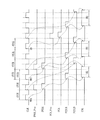
図3は図2のカラム選択線信号生成装置の動作を説明するための動作タイミング図である。 FIG. 3 is an operation timing chart for explaining the operation of the column selection line signal generation device of FIG.
図3を参照すると、動作クロックCLK、動作活性化信号のライト活性化信号PWAX及びリード活性化信号PCA、カラム選択線イネーブル信号PCSLE、カラム選択線ディスエーブル信号PCSLD及びカラム選択線信号CSL、第1動作モードM1及び第2動作モードM2が図示される。コマンドCMDは具体的な動作命令のライト命令WR1,WR2及びリード命令RDで示す。 Referring to FIG. 3, the operation clock CLK, the write activation signal PWAX of the operation activation signal and the read activation signal PCA, the column selection line enable signal PCSLE, the column selection line disable signal PCSLD and the column selection line signal CSL, An operation mode M1 and a second operation mode M2 are illustrated. The command CMD is indicated by a write command WR1, WR2 and a read command RD as specific operation commands.
メモリセルにデータがライトされるためにはライト命令WR1が印加され、動作クロックCLKでの動作クロックサイクル1TCKに応じてライト活性化信号PWAXが生成される。 In order to write data to the memory cell, a write command WR1 is applied, and a write activation signal PWAX is generated according to an operation clock cycle 1TCK at the operation clock CLK.
ライト活性化信号PWAXに応じてカラム選択線イネーブル信号PCSLEが生成され、カラム選択線イネーブル信号PCSLEによりカラム選択線信号CSLが活性化される。カラム選択線イネーブル信号PCSLEに応じてカラム選択線信号CSLが活性されることは第1動作モードM1と第2動作モードM2において同一である。 A column selection line enable signal PCSLE is generated in response to the write activation signal PWAX, and the column selection line signal CSL is activated by the column selection line enable signal PCSLE. The column selection line signal CSL is activated in response to the column selection line enable signal PCSLE in the first operation mode M1 and the second operation mode M2.
そして、動作クロックサイクルよりも1動作クロックサイクル以後の第2動作クロックサイクルに応じてクロック選択線ディスエーブル信号PCSLDが生成される。 Then, the clock selection line disable signal PCSLD is generated in accordance with the second operation clock cycle after one operation clock cycle rather than the operation clock cycle.
まず、コマンドCMDがライト命令WR1に連続して印加される場合に第1動作モードM1は、ライト命令WR1が応ずる動作クロックサイクル1TCKより2動作クロックサイクル以後の第3動作クロックサイクル3TCKに応じてライト活性化信号PWAXが生成されるモードである。即ち、第1動作モードM1はライト命令WR2が印加され、第3動作クロックサイクル3TCKに応じてライト活性化信号PWAXが生成される場合、ライト活性化信号PWAXに応じてカラム選択線信号が遷移されるモードである。第1区間制御信号はライト活性化信号PWAXにより生成された信号(図2のINPUT2)であり、カラム選択線信号CSLの第1動作モードのパルス区間を決定する。 First, when the command CMD is continuously applied to the write command WR1, the first operation mode M1 is written in accordance with the third operation clock cycle 3TCK after two operation clock cycles from the operation clock cycle 1TCK to which the write command WR1 responds. In this mode, the activation signal PWAX is generated. That is, in the first operation mode M1, when the write command WR2 is applied and the write activation signal PWAX is generated according to the third operation clock cycle 3TCK, the column selection line signal is transitioned according to the write activation signal PWAX. Mode. The first section control signal is a signal (INPUT2 in FIG. 2) generated by the write activation signal PWAX, and determines the pulse section of the first operation mode of the column selection line signal CSL.
第3動作クロックサイクル3TCKはライト命令WR2が応ずる動作クロックサイクルであるため、続くリード命令RDとの関係では第1動作クロックサイクル1TCKと同一視することができる。即ち、第2動作モードM2では第1動作クロックサイクル1TCKとして見ることができる。図3で第2動作モードM2と関係する動作クロックサイクル1TCK,2TCK,3TCK,4TCKはそのような意味で用いた。 Since the third operation clock cycle 3TCK is an operation clock cycle to which the write command WR2 responds, the third operation clock cycle 3TCK can be identified with the first operation clock cycle 1TCK in relation to the subsequent read command RD. That is, in the second operation mode M2, it can be viewed as the first operation clock cycle 1TCK. In FIG. 3, the operation clock cycles 1TCK, 2TCK, 3TCK, and 4TCK related to the second operation mode M2 are used in this sense.
次いで、コマンドCMDがライト命令WR2に連続して印加されない場合の第2動作モードM2は第3動作クロックサイクル以後の第4動作クロックサイクルに応じてコマンドCMD(図3のRD)が印加されるモードである。即ち、第2動作モードはライト命令WR2が印加された後、ライト命令WR2が応ずる動作クロックサイクルの次の動作クロックサイクル2TCKに応じて生成されたディスエーブル信号のカラム選択線ディスエーブル信号PCSLDにより遷移されるモードである。ここで、第2区間制御信号はカラム選択線ディスエーブル信号PCSLDにより生成された信号であって、カラム選択線信号CSLの第2動作モードM2のパルス区間を決定する。カラム選択線ディスエーブル信号PCSLDは追加的な遅延回路を含んでもよい。 Next, the second operation mode M2 when the command CMD is not continuously applied to the write command WR2 is a mode in which the command CMD (RD in FIG. 3) is applied according to the fourth operation clock cycle after the third operation clock cycle. It is. That is, the second operation mode is changed by the column selection line disable signal PCSLD of the disable signal generated in response to the operation clock cycle 2TCK next to the operation clock cycle to which the write command WR2 responds after the write command WR2 is applied. Mode. Here, the second interval control signal is a signal generated by the column selection line disable signal PCSLD, and determines the pulse interval of the second operation mode M2 of the column selection line signal CSL. The column select line disable signal PCSLD may include an additional delay circuit.
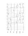
図4は本発明の好適な他の実施形態によるカラム選択線信号生成装置の動作を説明するための動作タイミング図である。 FIG. 4 is an operation timing diagram for explaining an operation of the column selection line signal generating apparatus according to another preferred embodiment of the present invention.
図4を参照すると、カラム選択線信号生成装置はプリコマンドパルスPWAX_Pre,PCA_Preに応じて第1区間制御信号を出力し、カラム選択線ディスエーブル信号に応じて第2区間制御信号を出力する区間制御信号生成部を備える。即ち、カラム選択線信号生成装置でのカラム選択線信号生成部はコマンド(図1のCMD)がライト命令WR1に連続して印加される場合には第1動作モードM1を有し、コマンド(図1のCMD)がライト命令WR2に連続して印加されない場合には第2動作モードM2を有し、コマンド(図1のCMD)により生成されたイネーブル信号が入力される場合、第1,2区間制御信号に応じて第1,2動作モードM1,M2で互いに異なったパルス区間を有するカラム選択線信号を生成する。そして、カラム選択線信号生成装置での区間制御信号生成部は第1動作モードM1ではコマンドCMDが印加される動作クロックサイクル1TCKの次の動作クロックサイクルの第2動作クロックサイクル2TCKと遷移時点が大抵一致するプリコマンドパルスPWAX_Pre,PCA_Preに応じて第1区間制御信号を出力し、第2動作モードM2ではディスエーブル信号に応じて第2区間制御信号を第1区間制御信号の遷移時点とは異にして出力する。ディスエーブル信号は第2動作クロックサイクル2TCKに応じて生成されるカラム選択線ディスエーブル信号PCSLDである。 Referring to FIG. 4, the column selection line signal generator outputs a first interval control signal according to pre-command pulses PWAX_Pre and PCA_Pre, and outputs a second interval control signal according to a column selection line disable signal. A signal generation unit is provided. That is, the column selection line signal generation unit in the column selection line signal generation apparatus has the first operation mode M1 when the command (CMD in FIG. 1) is applied continuously to the write command WR1, and the command (FIG. 1 CMD) is not continuously applied to the write command WR2, the second operation mode M2 is provided, and when the enable signal generated by the command (CMD in FIG. 1) is input, the first and second sections In response to the control signal, column selection line signals having different pulse sections in the first and second operation modes M1 and M2 are generated. In the first operation mode M1, the section control signal generation unit in the column selection line signal generation device usually has a transition time point that is the second operation clock cycle 2TCK of the operation clock cycle 1TCK to which the command CMD is applied. The first section control signal is output in accordance with the matching pre-command pulses PWAX_Pre and PCA_Pre, and in the second operation mode M2, the second section control signal is made different from the transition point of the first section control signal in accordance with the disable signal. Output. The disable signal is a column selection line disable signal PCSLD generated in response to the second operation clock cycle 2TCK.
第1動作モードM1でプリコマンドパルスPWAX_Pre,PCA_Preはカラム選択線ディスエーブル信号PCSLDよりも先に生成されることが好ましい。そこで、カラム選択線ディスエーブル信号PCSLDは遅延セルDCによりプリコマンドパルスPWAX_Pre,PCA_Preよりも遅く生成されることが好ましい。 In the first operation mode M1, it is preferable that the pre-command pulses PWAX_Pre and PCA_Pre are generated before the column selection line disable signal PCSLD. Therefore, the column selection line disable signal PCSLD is preferably generated later than the pre-command pulses PWAX_Pre and PCA_Pre by the delay cell DC.
第2動作モードM2でプリコマンドパルスPWAX_Pre,PCA_Preはカラム選択線ディスエーブル信号PCSLDよりも遅く生成されることが好ましい。これはカラム選択線信号CSLの遷移がプリコマンドパルスPWAX_Pre,PCA_Preとカラム選択線ディスエーブル信号のうち早い信号に応じて遷移されるからである。 In the second operation mode M2, the pre-command pulses PWAX_Pre and PCA_Pre are preferably generated later than the column selection line disable signal PCSLD. This is because the transition of the column selection line signal CSL is transitioned in response to an early signal among the pre-command pulses PWAX_Pre and PCA_Pre and the column selection line disable signal.
そして、第2区間制御信号の遷移時点は第1区間遷移時点よりも一層遅くなるため、カラム選択線信号CSLのパルス幅は第2動作モードM2で一層広くなる。 Since the transition time of the second interval control signal is much later than the first interval transition time, the pulse width of the column selection line signal CSL becomes wider in the second operation mode M2.
本発明の好適な更に他の実施形態は一つのアクセストランジスタとストレージキャパシタからなる単位メモリセルが行と列の交差点にマトリックス形態に連結されたメモリブロックを複数個だけ有するメモリセルアレイと、メモリセルの行を選択するためのロー選択回路と、コマンドCMDがライト命令WR1,WR2に連続して印加される場合には第1動作モードM1を有し、コマンドCMDがライト命令WR1,WR2に連続して印加されない場合には第2動作モードM2を有し、イネーブル信号が入力される場合に第1,2区間制御信号に応じて第1,2動作モードM1,M2で互いに異なったパルス区間を有するカラム選択線信号を生成するカラム選択線信号生成部と、第1動作モードM1では第1区間制御信号を出力し、第2動作モードM2では第1区間制御信号の遷移時点とは異なった第2区間制御信号を出力する区間制御信号生成部と、を備えて、メモリセルの列を選択するためのカラム選択回路を有する半導体メモリ装置として具体化される。ここで、イネーブル信号は動作クロックサイクルに応じて印加されたコマンドCMDにより生成される動作活性化信号PWAX,PCAに応じて生成されるカラム選択線イネーブル信号PCSLEである。そして、第1区間制御信号はコマンドに応じて遷移され、第2区間制御信号は動作クロックサイクルの次の動作クロックサイクルの第2動作クロックサイクルにより生成されたディスエーブル信号のカラム選択線ディスエーブル信号PCSLDに応じて遷移される。そして、コマンドは第1動作モードM1で第2動作クロックサイクルの次の動作クロックサイクルの第3動作クロックサイクルに応じて印加され、第2動作モードM2で第3動作クロックサイクル以後の第4動作クロックサイクルに応じて印加される。 According to still another preferred embodiment of the present invention, a memory cell array having a plurality of memory blocks in which unit memory cells each consisting of one access transistor and a storage capacitor are connected in a matrix at the intersection of a row and a column, A row selection circuit for selecting a row, and when the command CMD is continuously applied to the write commands WR1 and WR2, the first operation mode M1 is provided, and the command CMD is continuously input to the write commands WR1 and WR2. A column having a second operation mode M2 when not applied, and having a different pulse section in the first and second operation modes M1 and M2 according to the first and second section control signals when an enable signal is input. In the first operation mode M1, the first section control signal is output and the second operation is performed in the column selection line signal generation unit that generates the selection line signal. And a section control signal generator for outputting a second section control signal different from the transition point of the first section control signal, and a semiconductor having a column selection circuit for selecting a column of memory cells. It is embodied as a memory device. Here, the enable signal is a column selection line enable signal PCSLE generated according to the operation activation signals PWAX and PCA generated by the command CMD applied according to the operation clock cycle. The first interval control signal is transitioned according to the command, and the second interval control signal is the disable signal column select line disable signal generated by the second operation clock cycle of the operation clock cycle following the operation clock cycle. Transition is made according to the PCSLD. The command is applied in accordance with the third operation clock cycle of the operation clock cycle next to the second operation clock cycle in the first operation mode M1, and the fourth operation clock after the third operation clock cycle in the second operation mode M2. Applied according to the cycle.
本発明の好適な更に他の実施形態によるデータアクセスのためにメモリセルと連結されるカラムラインを選択するカラム選択回路を備えた半導体メモリ装置でのカラム選択線信号生成方法は、データアクセスのためのコマンドCMDが設定された連続ウィンド区間内でライト命令に連続して印加されるかどうかに従い、互いに異なったパルス区間を有するカラム選択線信号を差別的に生成する。ここで、連続ウィンド区間はコマンドが応答する動作クロックサイクルから動作クロックサイクルよりも2サイクル以前の動作クロックサイクルに応じてライト命令が入力される区間である。 According to another exemplary embodiment of the present invention, a column selection line signal generation method in a semiconductor memory device having a column selection circuit that selects a column line connected to a memory cell for data access is provided for data access. The column selection line signals having different pulse sections are generated differently according to whether or not the command CMD is continuously applied to the write command within the set continuous window section. Here, the continuous window section is a section in which a write command is input in accordance with an operation clock cycle two cycles before the operation clock cycle from the operation clock cycle to which the command responds.
図5は図2によるカラム選択線信号生成装置により、従来よりも速くなったメモリセルへのデータライト時点を示す動作タイミング図である。 FIG. 5 is an operation timing chart showing the time of data write to the memory cell, which is faster than the prior art by the column selection line signal generation device of FIG.
図5を参照すると、コマンド(例えばライトWR)が印加されて動作クロックCLKに応じてカラム選択線信号CSLが生成される。具体的な内部応答及び信号生成の関係は図3または図4での説明と同様なので省略する。 Referring to FIG. 5, a command (for example, write WR) is applied, and a column selection line signal CSL is generated according to the operation clock CLK. The specific relationship between internal response and signal generation is the same as that described with reference to FIG. 3 or FIG.
カラム選択線信号CSLによりIOドライバ/MUXのイネーブル信号のPDT信号が生成される。そして、コマンドが応答する動作クロックサイクルよりも1サイクル以後の動作クロックサイクルに応じてカラム選択線信号CSLが遷移される。カラム選択線信号CSLの遷移時点が図3及び図4に説明したように第1動作モード801と第2動作モード802で互いに異なる。その結果、IOドライバ/MUX経路が連結される時間が更に長くなる。従って、メモリセルに最後のデータがライトされる時点が第1動作モード時803と第2動作モード時813において異なる。即ち、第2動作モード時に最後データが更に速くライトされる。よって、最後データがメモリセルに完全にライトされた後にビットラインのプリチャージが行われることにより、データの損傷が減少する。
The PDT signal of the IO driver / MUX enable signal is generated by the column selection line signal CSL. Then, the column selection line signal CSL transitions in accordance with an operation clock cycle after one cycle from the operation clock cycle to which the command responds. The transition point of the column selection line signal CSL is different between the
本発明の好適な実施形態による半導体メモリ装置のカラム選択線信号生成装置は上記の実施形態に限定されず、本発明の基本原理を逸脱しない範囲内で多様に設計され且つ応用されることは、当業者には自明な事実である。 The column selection line signal generation apparatus of the semiconductor memory device according to the preferred embodiment of the present invention is not limited to the above-described embodiment, and can be variously designed and applied without departing from the basic principle of the present invention. This is obvious to those skilled in the art.
122:コマンドバッファ
124:カラム選択線イネーブル部
125:カラム選択線ディスエーブル部
CMD:コマンド
127:PDT発生器
128:IOドライバ/MUX
129:ビットラインセンスアンプ
MC:メモリセル
201:カラム選択線信号生成装置
200:可変カラム選択線ドライバ
130:遅延セル
DC:遅延セル
M1:第1動作モード
M2:第2動作モード
PWAX:ライト活性化信号
PCA:リード活性化信号
PWAX_Pre,PCA_Pre:プリコマンドパルス
122: Command buffer 124: Column selection line enable unit 125: Column selection line disable unit CMD: Command 127: PDT generator 128: IO driver / MUX
129: Bit line sense amplifier MC: Memory cell 201: Column selection line signal generator 200: Variable column selection line driver 130: Delay cell DC: Delay cell M1: First operation mode M2: Second operation mode PWAX: Write activation Signal PCA: Read activation signal PWAX_Pre, PCA_Pre: Pre-command pulse
Claims (23)
コマンドがライト命令に連続して印加される場合には第1動作モードを有し、前記コマンドが前記ライト命令に連続して印加されない場合には第2動作モードを有し、カラム選択線イネーブル信号によりカラム選択線信号がイネーブルされ、前記カラム選択線信号の動作区間は前記第1及び第2動作モードで互いに異なることを特徴とするカラム選択線信号生成装置。 In a column selection line signal generation device of a semiconductor memory device,
When the command is applied continuously to the write command, the first operation mode is provided. When the command is not applied consecutively to the write command, the second operation mode is provided. The column selection line signal generation device according to claim 1, wherein a column selection line signal is enabled, and an operation period of the column selection line signal is different between the first and second operation modes.
前記第1動作モードでは前記動作活性化信号に応じて前記第1区間制御信号を出力し、前記第2動作モードではカラム選択線ディスエーブル信号に応じて前記第1区間制御信号の遷移時点よりも遅い前記第2区間制御信号を出力する区間制御信号生成部と、を備えることを特徴とする請求項2に記載のカラム選択線信号生成装置。 The column selection line signal generating device generates a column selection line signal having different operation sections according to first and second section control signals when the column selection line enable signal is input. A generator,
In the first operation mode, the first section control signal is output in response to the operation activation signal, and in the second operation mode, the transition period of the first section control signal is in response to a column selection line disable signal. The column selection line signal generation device according to claim 2, further comprising: a section control signal generation unit that outputs the second section control signal that is slow.
前記第1動作モードでは前記コマンドが印加される動作クロックサイクルの次の動作クロックサイクルの遷移時点と略一致するプリコマンドパルスに応じて前記第1区間制御信号を出力し、前記第2動作モードではディスエーブル信号に応じて前記第2区間制御信号を前記第1区間制御信号の遷移時点とは異にして出力する区間制御信号生成部と、を備えることを特徴とするカラム選択線信号生成装置。 In a column selection line signal generation device of a semiconductor memory device, the first operation mode is provided when a command is applied continuously to a write command, and the first operation mode is applied when the command is not applied continuously to the write command. Columns having two operation modes and having different pulse sections in the first and second operation modes according to the first and second section control signals when the column selection line enable signal generated by the command is input A column selection line signal generator for generating a selection line signal;
In the first operation mode, the first section control signal is output in response to a pre-command pulse substantially coincident with the transition point of the operation clock cycle next to the operation clock cycle to which the command is applied. In the second operation mode, A column selection line signal generation device comprising: an interval control signal generation unit that outputs the second interval control signal in response to a disable signal different from the transition time of the first interval control signal.
前記メモリセルの行を選択するためのロー選択回路と、
コマンドがライト命令に連続して印加される場合には第1動作モードを有し、前記コマンドが前記ライト命令に連続して印加されない場合には第2動作モードを有し、カラム選択線イネーブル信号によりイネーブルされ、前記第1及び第2動作モードで互いに異なった動作区間を有するカラム選択線信号により前記メモリセルの列を選択するためのカラム選択回路を有することを特徴とする半導体メモリ装置。 A memory cell array having a plurality of memory blocks in which unit memory cells each consisting of one access transistor and a storage capacitor are connected in a matrix at the intersection of a row and a column;
A row selection circuit for selecting a row of the memory cells;
When the command is applied continuously to the write command, the first operation mode is provided. When the command is not applied consecutively to the write command, the second operation mode is provided. And a column selection circuit for selecting a column of the memory cells according to a column selection line signal which is enabled by the above and has different operation sections in the first and second operation modes.
前記第1動作モードでは前記動作活性化信号に応じて前記第1区間制御信号を出力し、前記第2動作モードではカラム選択線ディスエーブル信号に応じて前記第1区間制御信号の遷移時点よりも遅い前記第2区間制御信号を出力する区間制御信号生成部と、を備えることを特徴とする請求項13に記載の半導体メモリ装置。 A column selection line signal generator for generating column selection line signals having different operation intervals according to the first and second interval control signals when the column selection line enable signal is input;
In the first operation mode, the first section control signal is output in response to the operation activation signal, and in the second operation mode, the transition period of the first section control signal is in response to a column selection line disable signal. The semiconductor memory device of claim 13, further comprising: a section control signal generation unit that outputs the second section control signal that is late.
前記データアクセスのためのコマンドが設定された連続ウィンド区間内でライト命令に連続して印加されるかどうかをチェックする連続判定部と、
前記連続判定部に動作的に連結され、前記連続するかどうかに従い互いに異なったパルス区間を有するカラム選択線信号を差別的に生成する信号生成部と、を備えることを特徴とするカラム線選択信号生成回路。 In a column line selection signal generation circuit in a semiconductor memory device using a column selection line signal for selecting a column line connected to a memory cell for data access,
A continuous determination unit that checks whether the command for data access is continuously applied to a write command within a set continuous window section;
A column line selection signal, comprising: a signal generation unit that is operatively connected to the continuity determination unit and that differentially generates column selection line signals having different pulse intervals depending on whether the continuation unit is continuous. Generation circuit.
前記データアクセスのためのコマンドが設定された連続ウィンド区間内でライト命令に連続して印加されるかどうかに従い、互いに異なったパルス区間を有するカラム選択線信号を差別的に生成することを特徴とするカラム選択線信号生成方法。 In a column selection line signal generation method in a semiconductor memory device including a column selection circuit that selects a column line connected to a memory cell for data access,
According to whether the command for data access is continuously applied to a write command within a set continuous window period, a column selection line signal having different pulse periods is generated differentially. Column selection line signal generation method.
Applications Claiming Priority (2)
| Application Number | Priority Date | Filing Date | Title |
|---|---|---|---|
| KR10-2004-0104713 | 2004-12-13 | ||
| KR1020040104713A KR100610018B1 (en) | 2004-12-13 | 2004-12-13 | Column select line signal generator of a semiconductor memory device |
Publications (3)
| Publication Number | Publication Date |
|---|---|
| JP2006172702A true JP2006172702A (en) | 2006-06-29 |
| JP2006172702A5 JP2006172702A5 (en) | 2008-11-27 |
| JP5037006B2 JP5037006B2 (en) | 2012-09-26 |
Family
ID=36583628
Family Applications (1)
| Application Number | Title | Priority Date | Filing Date |
|---|---|---|---|
| JP2005359515A Expired - Fee Related JP5037006B2 (en) | 2004-12-13 | 2005-12-13 | Column selection line signal generation device for semiconductor memory device |
Country Status (3)
| Country | Link |
|---|---|
| US (1) | US7295488B2 (en) |
| JP (1) | JP5037006B2 (en) |
| KR (1) | KR100610018B1 (en) |
Families Citing this family (19)
| Publication number | Priority date | Publication date | Assignee | Title |
|---|---|---|---|---|
| KR100821573B1 (en) * | 2006-04-05 | 2008-04-15 | 주식회사 하이닉스반도체 | Column selection signal generator of semiconductor memory |
| DE102006029169B4 (en) * | 2006-06-24 | 2009-03-26 | Qimonda Ag | Memory chip with changeable column selection duration |
| KR100868251B1 (en) * | 2007-03-22 | 2008-11-12 | 주식회사 하이닉스반도체 | Semiconductor memory device |
| KR100852002B1 (en) * | 2007-05-14 | 2008-08-13 | 주식회사 하이닉스반도체 | Pulse Width Control Circuit of Column Selection Signal of Semiconductor Memory Device |
| KR100881134B1 (en) * | 2007-06-27 | 2009-02-02 | 주식회사 하이닉스반도체 | Column access control unit |
| KR100924347B1 (en) * | 2008-01-03 | 2009-10-30 | 주식회사 하이닉스반도체 | Column selection signal control device and method |
| KR100967112B1 (en) * | 2008-11-10 | 2010-07-05 | 주식회사 하이닉스반도체 | Output Enable Signal Generation Circuit |
| KR100980061B1 (en) | 2008-12-23 | 2010-09-03 | 주식회사 하이닉스반도체 | Control signal generation circuit |
| KR101020290B1 (en) * | 2009-01-12 | 2011-03-07 | 주식회사 하이닉스반도체 | Burst Mode Control Circuit |
| KR101047003B1 (en) | 2009-06-26 | 2011-07-06 | 주식회사 하이닉스반도체 | Precharge signal generation circuit and semiconductor memory device |
| KR101052078B1 (en) * | 2010-02-26 | 2011-07-27 | 주식회사 하이닉스반도체 | Semiconductor memory device and operation method thereof |
| US9563253B2 (en) | 2013-03-12 | 2017-02-07 | Intel Corporation | Techniques for power saving on graphics-related workloads |
| US9715909B2 (en) | 2013-03-14 | 2017-07-25 | Micron Technology, Inc. | Apparatuses and methods for controlling data timing in a multi-memory system |
| KR102686058B1 (en) * | 2016-09-06 | 2024-07-17 | 에스케이하이닉스 주식회사 | Semiconductor device |
| US11462261B2 (en) * | 2019-10-10 | 2022-10-04 | Micron Technology, Inc. | Methods of activating input/output lines of memory devices, and related devices and systems |
| US11715503B2 (en) | 2021-03-26 | 2023-08-01 | Changxin Memory Technologies, Inc. | Signal generation circuit and memory |
| CN116072170B (en) | 2021-11-03 | 2025-06-27 | 长鑫存储技术有限公司 | Memory read-write circuit, memory control method and electronic device |
| CN116072169B (en) * | 2021-11-03 | 2025-06-27 | 长鑫存储技术有限公司 | Memory read-write circuit, memory control method and electronic equipment |
| TWI849542B (en) * | 2022-10-20 | 2024-07-21 | 晶豪科技股份有限公司 | Method and circuit for adaptive column-select line signal generation |
Citations (2)
| Publication number | Priority date | Publication date | Assignee | Title |
|---|---|---|---|---|
| JPH09167489A (en) * | 1995-11-13 | 1997-06-24 | Samsung Electron Co Ltd | Column selection signal control circuit |
| JP2003331579A (en) * | 2002-04-27 | 2003-11-21 | Samsung Electronics Co Ltd | Method and apparatus for controlling column decoder enable timing of synchronous semiconductor memory device |
Family Cites Families (7)
| Publication number | Priority date | Publication date | Assignee | Title |
|---|---|---|---|---|
| US6038176A (en) * | 1997-12-10 | 2000-03-14 | Winbond Electronics Corporation | Presettable semiconductor memory device |
| JPH11306758A (en) * | 1998-04-27 | 1999-11-05 | Matsushita Electric Ind Co Ltd | Semiconductor storage device |
| JP2000021198A (en) * | 1998-06-30 | 2000-01-21 | Mitsubishi Electric Corp | Synchronous semiconductor integrated circuit device |
| JP2003059264A (en) * | 2001-08-08 | 2003-02-28 | Hitachi Ltd | Semiconductor storage device |
| US6972978B1 (en) * | 2002-03-15 | 2005-12-06 | Integrated Device Technology, Inc. | Content addressable memory (CAM) devices with block select and pipelined virtual sector look-up control and methods of operating same |
| ITMI20021540A1 (en) | 2002-07-12 | 2004-01-12 | St Microelectronics Srl | BUCK TYPE MULTI-PHASE VOLTAGE REGULATOR |
| JP2004178729A (en) * | 2002-11-28 | 2004-06-24 | Hitachi Ltd | Semiconductor storage device |
-
2004
- 2004-12-13 KR KR1020040104713A patent/KR100610018B1/en not_active Expired - Fee Related
-
2005
- 2005-11-14 US US11/272,900 patent/US7295488B2/en not_active Expired - Fee Related
- 2005-12-13 JP JP2005359515A patent/JP5037006B2/en not_active Expired - Fee Related
Patent Citations (2)
| Publication number | Priority date | Publication date | Assignee | Title |
|---|---|---|---|---|
| JPH09167489A (en) * | 1995-11-13 | 1997-06-24 | Samsung Electron Co Ltd | Column selection signal control circuit |
| JP2003331579A (en) * | 2002-04-27 | 2003-11-21 | Samsung Electronics Co Ltd | Method and apparatus for controlling column decoder enable timing of synchronous semiconductor memory device |
Also Published As
| Publication number | Publication date |
|---|---|
| KR100610018B1 (en) | 2006-08-08 |
| JP5037006B2 (en) | 2012-09-26 |
| US7295488B2 (en) | 2007-11-13 |
| KR20060066203A (en) | 2006-06-16 |
| US20060126421A1 (en) | 2006-06-15 |
Similar Documents
| Publication | Publication Date | Title |
|---|---|---|
| JP5037006B2 (en) | Column selection line signal generation device for semiconductor memory device | |
| US6459641B2 (en) | Semiconductor memory device | |
| JP2003249077A (en) | Semiconductor memory device and its control method | |
| JP3604291B2 (en) | Memory device with double-rate input / output circuit | |
| JP4307894B2 (en) | Method and apparatus for controlling column decoder enable timing of synchronous semiconductor memory device | |
| US6205069B1 (en) | Semiconductor memory device with fast input/output line precharge scheme and method of precharging input/output lines thereof | |
| US8730742B2 (en) | Device | |
| JPH1040678A (en) | Semiconductor memory | |
| KR100566615B1 (en) | Semiconductor memory | |
| KR20050015853A (en) | Semiconductor device and method for controlling the same | |
| KR100430658B1 (en) | Semiconductor memory device operable for both of cas latencies of one and more than one | |
| KR100473747B1 (en) | Semiconductor memory device that operates in synchronization with a clock signal | |
| US7145820B2 (en) | Semiconductor memory device for reducing chip area | |
| KR20100117874A (en) | Precharge method of semiconductor memory device for contorlling precharge starting time of each bank at bank precharge operation and semiconductor memory device using it | |
| KR100359360B1 (en) | Semiconductor memory device | |
| US20080002498A1 (en) | Semiconductor memory device and driving method thereof | |
| JP4143287B2 (en) | Semiconductor memory device and data read control method thereof | |
| KR100405582B1 (en) | Synchronous semiconductor memory device | |
| US6483762B1 (en) | tRCD margin | |
| KR20010077080A (en) | Burst-type semiconductor memory device having full-page mode | |
| US20200302992A1 (en) | Memory device with improved writing features | |
| US6415399B1 (en) | Semiconductor memory device requiring performance of plurality of tests for each of plurality of memory circuits and method for testing the same | |
| KR100481819B1 (en) | SRAM compatible and Synchronous Memory Device being controlled by a signal, the signal activating in Chip disable period | |
| US7359267B2 (en) | Method of transferring data | |
| KR20050032892A (en) | Semiconductor memory device able to read and write at a time |
Legal Events
| Date | Code | Title | Description |
|---|---|---|---|
| RD03 | Notification of appointment of power of attorney |
Free format text: JAPANESE INTERMEDIATE CODE: A7423 Effective date: 20080201 |
|
| RD04 | Notification of resignation of power of attorney |
Free format text: JAPANESE INTERMEDIATE CODE: A7424 Effective date: 20080620 |
|
| A521 | Request for written amendment filed |
Free format text: JAPANESE INTERMEDIATE CODE: A523 Effective date: 20081008 |
|
| A621 | Written request for application examination |
Free format text: JAPANESE INTERMEDIATE CODE: A621 Effective date: 20081008 |
|
| A977 | Report on retrieval |
Free format text: JAPANESE INTERMEDIATE CODE: A971007 Effective date: 20110531 |
|
| A131 | Notification of reasons for refusal |
Free format text: JAPANESE INTERMEDIATE CODE: A131 Effective date: 20110823 |
|
| A521 | Request for written amendment filed |
Free format text: JAPANESE INTERMEDIATE CODE: A523 Effective date: 20111122 |
|
| TRDD | Decision of grant or rejection written | ||
| A01 | Written decision to grant a patent or to grant a registration (utility model) |
Free format text: JAPANESE INTERMEDIATE CODE: A01 Effective date: 20120605 |
|
| A01 | Written decision to grant a patent or to grant a registration (utility model) |
Free format text: JAPANESE INTERMEDIATE CODE: A01 |
|
| A61 | First payment of annual fees (during grant procedure) |
Free format text: JAPANESE INTERMEDIATE CODE: A61 Effective date: 20120704 |
|
| FPAY | Renewal fee payment (event date is renewal date of database) |
Free format text: PAYMENT UNTIL: 20150713 Year of fee payment: 3 |
|
| R150 | Certificate of patent or registration of utility model |
Free format text: JAPANESE INTERMEDIATE CODE: R150 |
|
| LAPS | Cancellation because of no payment of annual fees |