JP2006190868A - Semiconductor memory device - Google Patents
Semiconductor memory device Download PDFInfo
- Publication number
- JP2006190868A JP2006190868A JP2005002259A JP2005002259A JP2006190868A JP 2006190868 A JP2006190868 A JP 2006190868A JP 2005002259 A JP2005002259 A JP 2005002259A JP 2005002259 A JP2005002259 A JP 2005002259A JP 2006190868 A JP2006190868 A JP 2006190868A
- Authority
- JP
- Japan
- Prior art keywords
- diffusion layer
- memory device
- semiconductor memory
- charge holding
- region
- Prior art date
- Legal status (The legal status is an assumption and is not a legal conclusion. Google has not performed a legal analysis and makes no representation as to the accuracy of the status listed.)
- Pending
Links
Images


Landscapes
- Semiconductor Memories (AREA)
- Non-Volatile Memory (AREA)
Abstract
【課題】素子の微細化(高集積化)と信頼性の高い安定した高速メモリ動作ができ、2ビット以上の記憶保持ができる半導体記憶装置を提供する。
【解決手段】半導体基板10上に第1,第2の拡散層領域17,18を形成し、その第1,第2の拡散層領域17,18を連結するようにチャネル形成領域31を形成する。上記チャネル形成領域31上にゲート絶縁膜12を形成し、そのゲート絶縁膜12上にゲート電極13を形成する。また、上記ゲート絶縁膜12およびゲート電極13の両側の側壁に電荷保持体61,62を形成する。上記チャネル形成領域31にカーボンナノチューブを用いる。
【選択図】図1To provide a semiconductor memory device capable of miniaturization (high integration) of an element, a stable and high-speed memory operation with high reliability, and capable of storing and storing 2 bits or more.
First and second diffusion layer regions 17 and 18 are formed on a semiconductor substrate 10 and a channel formation region 31 is formed so as to connect the first and second diffusion layer regions 17 and 18. . A gate insulating film 12 is formed on the channel formation region 31, and a gate electrode 13 is formed on the gate insulating film 12. Further, charge holding bodies 61 and 62 are formed on the side walls on both sides of the gate insulating film 12 and the gate electrode 13. Carbon nanotubes are used for the channel formation region 31.
[Selection] Figure 1
Description
本発明は、半導体記憶装置に関し、より詳細には、電荷量の変化を電流量に変換する機能を有する電界効果トランジスタを用いた半導体記憶装置に関する。 The present invention relates to a semiconductor memory device, and more particularly to a semiconductor memory device using a field effect transistor having a function of converting a change in charge amount into a current amount.
従来、半導体記憶装置としては、1つの電界効果トランジスタで2ビットの記憶が可能な不揮発性メモリがあり、この不揮発性メモリはサイファン・セミコンダクターズ・リミテッド社が開発したものである(例えば、特表2001−512290号公報(特許文献1)参照)。上記従来技術のメモリの構造と、書込み動作原理を以下に説明する。 Conventionally, as a semiconductor memory device, there is a non-volatile memory capable of storing 2 bits with one field effect transistor, and this non-volatile memory has been developed by Cyphan Semiconductors Ltd. Table 2001-512290 publication (patent document 1) reference). The structure of the above prior art memory and the write operation principle will be described below.
この半導体記憶装置は、図9に示すように、P型ウェル領域901上にゲート絶縁膜を介して形成されたゲート電極909、P型ウェル領域901表面に形成された第1のN型拡散層領域902および第2のN型拡散層領域903から構成される。上記ゲート絶縁膜は、シリコン酸化膜904,905の間にシリコン窒化膜906が挟まれたONO(Oxide Nitride Oxide)膜からなる。シリコン窒化膜906中には、第1および第2のN型拡散層領域902,903の端部付近に、それぞれ記憶保持部907,908が形成されている。
As shown in FIG. 9, the semiconductor memory device includes a
これらの記憶保持部907,908のそれぞれの個所での電荷の多寡をトランジスタのドレイン電流として読み出すことにより、1トランジスタで2ビットの情報を記憶させることができる。
By reading the amount of charge at each of the
次に、この半導体記憶装置における書込み動作方法を説明する。ここで、書込みとは、記憶保持部907,908に電子を注入することを指すこととする。特表2001−512290号公報では、右側の記憶保持部908に蓄積された電子を放出させるために、第2の拡散層領域903に5.5Vを、ゲート電極909に10Vを印加する方法が開示されている。これにより、2つある記憶保持部907,908の特定の側に書込みをすることができる。また、特定の側の消去および読出しを行う方法も開示されており、これらの方法を総合して2ビット動作が可能となっている。
Next, a write operation method in this semiconductor memory device will be described. Here, writing refers to injecting electrons into the
しかし、上記半導体記憶装置のように、一般にMOSFET(Metal Oxide Semiconductor Field Effect Transistor:メタル・オキサイド・セミコンダクタ・電界効果トランジスタ)に基づいたメモリ素子は、繰り返し多数回の読み出し・書き込みおよび消去のメモリ動作を行うと、チャネルの移動度劣化が生じ、メモリ動作に必要な読み出し電流を保つことができず、信頼性の高い安定したメモリ動作を得ることができなかった。また、ゲート絶縁膜は、トランジスタを動作させるための機能と、電荷を蓄積するメモリ膜としての機能を併せ持たせるために、ONO膜の3層構造となっているため、ゲート絶縁膜の薄膜化が困難であった。 However, like the above-mentioned semiconductor memory devices, memory devices based on MOSFETs (Metal Oxide Semiconductor Field Effect Transistors) generally perform repeated read / write and erase memory operations many times. If this is done, the mobility of the channel deteriorates, the read current required for the memory operation cannot be maintained, and a reliable and stable memory operation cannot be obtained. In addition, since the gate insulating film has a three-layer structure of an ONO film in order to have both a function for operating the transistor and a function as a memory film for accumulating charges, the gate insulating film is thinned. It was difficult.
また、チャネル長が短くなるにつれ、1つのトランジスタの記憶保持部907,908の2箇所が互いに干渉して2ビット動作が困難なため、さらなる素子の微細化が果たせなかった。
そこで、本発明の目的は、素子の微細化(高集積化)と信頼性の高い安定した高速メモリ動作ができ、2ビット以上の記憶保持ができる半導体記憶装置を提供することにある。 SUMMARY OF THE INVENTION An object of the present invention is to provide a semiconductor memory device capable of miniaturization (high integration) of an element, a highly reliable and stable high-speed memory operation, and capable of storing and storing 2 bits or more.
上記課題を解決するため、本発明の半導体記憶装置は、複数の電荷保持体を有する多値記憶体と、上記多値記憶体の上記電荷保持体に夫々対応する拡散層領域と、上記多値記憶体の下側に配置され、上記拡散層領域を連結するチャネル形成領域とを備え、上記チャネル形成領域はカーボンナノチューブを含むことを特徴とする。ここで「多値」とは、4値以上の論理値をいう。 In order to solve the above problems, a semiconductor memory device according to the present invention includes a multi-value memory having a plurality of charge carriers, a diffusion layer region corresponding to each of the charge carriers of the multi-value memory, and the multi-values. And a channel forming region that is connected to the diffusion layer region, and the channel forming region includes carbon nanotubes. Here, “multi-value” means a logical value of four or more values.
上記構成の半導体記憶装置によれば、上記チャネル形成領域に、電気伝導度、熱伝導度の高い半導体性質を有するカーボンナノチューブを用いることにより、素子の微細化(高集積化)と信頼性の高い安定した高速メモリ動作を得ることができる。カーボンナノチューブ内を流れる電流は、トンネル効果によりほぼ抵抗無く流れるので、半導体記憶装置の読み出し・書き込みおよび消去のメモリ動作の高速化が可能となると共に、多数回のメモリ動作を繰り返し行うことでチャネルの移動度劣化が生じても、メモリ動作に必要な読み出し電流を保つことができ、長寿命で信頼性の高い安定したメモリ動作を得ることができる。また、カーボンナノチューブ内を流れる電流は、従来チャネル抵抗と同様かそれ以下で、上記電荷保持体に保持された電荷の影響を表すことになり、電荷の有無の判別を容易に行うことができ、多値の不揮発性メモリに適している。 According to the semiconductor memory device having the above configuration, the use of carbon nanotubes having a semiconductor property with high electrical conductivity and thermal conductivity in the channel formation region enables miniaturization of elements (high integration) and high reliability. A stable high-speed memory operation can be obtained. Since the current flowing through the carbon nanotube flows almost without resistance due to the tunnel effect, it is possible to speed up the memory operation of reading / writing and erasing of the semiconductor memory device, and by repeating the memory operation many times, Even when mobility deterioration occurs, a read current necessary for the memory operation can be maintained, and a stable memory operation with a long lifetime and high reliability can be obtained. In addition, the current flowing in the carbon nanotube is the same as or lower than the conventional channel resistance, and represents the influence of the charge held in the charge holding body, and can easily determine the presence or absence of charge, Suitable for multi-value nonvolatile memory.
また、上記構成の半導体記憶装置によれば、絶縁体あるいは絶縁体膜上にチャネル形成領域を設けることにより、半導体基板上にチャネル形成領域を形成する場合に比べ、リーク電流を抑制することができ、省電力の効果を得ることができる。また、完全素子分離ができ、拡散層領域の容量が低減できるため、集積密度や動作速度の向上が可能である。 Further, according to the semiconductor memory device having the above structure, by providing the channel formation region on the insulator or the insulator film, the leakage current can be suppressed as compared with the case where the channel formation region is formed on the semiconductor substrate. The power saving effect can be obtained. Further, since complete element isolation can be performed and the capacitance of the diffusion layer region can be reduced, integration density and operation speed can be improved.
また、一実施形態の半導体記憶装置は、上記多値記憶体が、基板上に形成されたゲート絶縁膜と、上記ゲート絶縁膜上に形成されたゲート電極とを有し、上記ゲート電極の側壁の両側に、上記多値記憶体の上記電荷保持体が2つ形成され、上記2つの電荷保持体の夫々に2つの上記拡散層領域が対応することを特徴とする。 In one embodiment, the multilevel memory includes a gate insulating film formed on a substrate and a gate electrode formed on the gate insulating film, and a sidewall of the gate electrode. Two charge holding bodies of the multi-value storage body are formed on both sides of the two, and the two diffusion layer regions correspond to the two charge holding bodies, respectively.
上記実施形態の半導体記憶装置によれば、従来のサイドウォール型のトランジスタとほぼ同じ構造であり、従来の作製方法で製造することができる。また、構造的に記憶部である2つの拡散層領域がゲート電極により分離されているので微細化が可能であり、ゲート・チャネル間を短くでき、低電圧でチャネルに高電界を加えることが可能である。 The semiconductor memory device of the above embodiment has almost the same structure as a conventional sidewall type transistor, and can be manufactured by a conventional manufacturing method. In addition, the two diffusion layer regions that are structurally separated by the gate electrode are separated by the gate electrode, so miniaturization is possible, the gap between the gate and the channel can be shortened, and a high electric field can be applied to the channel at a low voltage. It is.
また、一実施形態の半導体記憶装置は、上記電荷保持体が、電荷を蓄積する機能を有する第1の絶縁体と、上記第1の絶縁体を両側から挟むように配置された第2の絶縁体と第3の絶縁体とを有し、上記第1の絶縁体がシリコン窒化物または酸化アルミニウムであり、上記第2および第3の絶縁体がシリコン酸化物であることを特徴とする。 In one embodiment of the semiconductor memory device, the charge holding body includes a first insulator having a function of accumulating charges, and a second insulator disposed so as to sandwich the first insulator from both sides. And a third insulator, wherein the first insulator is silicon nitride or aluminum oxide, and the second and third insulators are silicon oxide.
上記実施形態の半導体記憶装置によれば、上記電荷を蓄積する機能を有する第1の絶縁体に用いられるシリコン窒化物(または酸化アルミニウム)は、電荷(電子および正孔)をトラップする準位が多数存在するため、大きなヒステリシス特性を得ることができ、半導体装置の製造工程で多く用いられている物質である。また、第2および第3の絶縁体にシリコン酸化物を用いることによって、シリコン窒化物(または酸化アルミニウム)に蓄積された電荷の漏れを防いでおり、また、上記電荷保持体はサンドウィッチ構造になっているので、電荷の注入効率が高くなり、書換え動作を高速化できる。 According to the semiconductor memory device of the above embodiment, the silicon nitride (or aluminum oxide) used for the first insulator having the function of accumulating charges has a level for trapping charges (electrons and holes). Since there are many, a large hysteresis characteristic can be obtained, and it is a substance often used in the manufacturing process of semiconductor devices. Further, by using silicon oxide for the second and third insulators, leakage of charges accumulated in silicon nitride (or aluminum oxide) is prevented, and the charge holding body has a sandwich structure. Therefore, the charge injection efficiency is increased, and the rewriting operation can be speeded up.
以上より明らかなように、本発明の半導体記憶装置によれば、チャネル形成領域に、電気伝導度、熱伝導度の高いカーボンナノチューブを用いることにより、素子の微細化(高集積化)と信頼性の高い安定した高速メモリ動作を得ることができる。 As can be seen from the above, according to the semiconductor memory device of the present invention, the use of carbon nanotubes with high electrical conductivity and high thermal conductivity in the channel formation region enables miniaturization (high integration) and reliability of the device. High and stable high-speed memory operation can be obtained.
また、カーボンナノチューブ内を流れる電流は、トンネル効果によりほぼ抵抗無く流れるので、半導体記憶装置の読み出し・書き込みおよび消去のメモリ動作の高速化が可能となり、また、多数回のメモリ動作を繰り返し行うことでチャネルの移動度劣化が生じても、メモリ動作に必要な読み出し電流を保つことができ、長寿命で信頼性の高い安定したメモリ動作を得ることができる。 In addition, since the current flowing through the carbon nanotube flows almost without resistance due to the tunnel effect, it is possible to speed up the memory operation of reading / writing and erasing of the semiconductor memory device, and by repeating the memory operation many times. Even when channel mobility is deteriorated, a read current necessary for memory operation can be maintained, and a stable memory operation with a long lifetime and high reliability can be obtained.
また、カーボンナノチューブ内を流れる電流が上記電荷保持体に保持された電荷の影響を表すことになり、電荷の有無の判別を容易に行うことができ、多値の不揮発性メモリに適している。 In addition, the current flowing in the carbon nanotube represents the influence of the charge held in the charge holding body, so that the presence / absence of charge can be easily determined, which is suitable for a multi-value nonvolatile memory.
また、上記チャネル形成領域に、電子の移動度がシリコンの電子の移動度より高い半導体を用いることにより、読み出し・書き込みおよび消去のメモリ動作を繰り返し多数回行うことなどによりチャネルの移動度劣化が生じても、メモリ動作に必要な読み出し電流を保つことができ、信頼性が高く長寿命で安定したメモリ動作を得ることができる。 In addition, by using a semiconductor whose electron mobility is higher than that of silicon in the channel formation region, channel mobility is deteriorated due to repeated read / write and erase memory operations. However, the read current necessary for the memory operation can be maintained, and a reliable and long-life and stable memory operation can be obtained.
また、本発明の半導体記憶装置では、書き込み後か消去後かの判別が容易にできるだけの電流差(書き込み後の読み出し電流と消去後の読み出し電流との電流差)を十分に保持していることから、大面積基板上にメモリを作製したとき、面内において作製ばらつきが生じ、書き込み後・消去後の読み出し電流値のメモリ性能ばらつきが生じても、メモリ動作に必要な書き込み後と消去後の読み出し電流差を得ることができるので、歩留まりをよくすることができ、生産性を向上することができる。また、絶縁体基板上にチャネル領域を設けることによって、完全素子分離ができ、また拡散層領域の容量が低減できるため、集積密度や動作速度の向上が可能である。 Further, in the semiconductor memory device of the present invention, the current difference (current difference between the read current after writing and the read current after erasing) as much as possible can be easily maintained so that it can be easily discriminated after writing or after erasing. Therefore, when a memory is manufactured on a large area substrate, manufacturing variations occur in the plane, and even if there is a variation in memory performance of read current values after writing and erasing, even after writing and erasing necessary for memory operation Since the read current difference can be obtained, the yield can be improved and the productivity can be improved. Further, by providing the channel region over the insulator substrate, complete element isolation can be performed and the capacity of the diffusion layer region can be reduced, so that the integration density and the operation speed can be improved.
また、従来のTFT(Thin Film Transistor:薄膜トランジスタ)のように絶縁体基板上に作製した半導体装置はチャネル形成領域にアモルファスシリコンやポリシリコンを用いているために移動度が低いという問題があったが、チャネル形成領域にカーボンナノチューブ(またはカーボンナノチューブと電子の移動度がシリコンの電子の移動度より高い半導体)を用いることにより、高速動作が可能な半導体装置を絶縁体基板上に作製することができる。 In addition, a semiconductor device manufactured on an insulator substrate such as a conventional thin film transistor (TFT) has a problem of low mobility because amorphous silicon or polysilicon is used for a channel formation region. A semiconductor device capable of high-speed operation can be manufactured over an insulator substrate by using carbon nanotubes (or a semiconductor whose electron mobility is higher than that of silicon electrons) in the channel formation region. .
また、本発明の半導体記憶装置は、従来の半導体プロセスを用いることができるので作製も容易である。 In addition, the semiconductor memory device of the present invention can be easily manufactured because a conventional semiconductor process can be used.
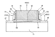
以下、本発明の半導体記憶装置を図示の実施の形態により詳細に説明する。図1,図2,図4,図5は本発明の実施の形態の半導体記憶装置の構造を示す概略断面図であり、図1に示す第1実施形態と図2に示す第2実施形態は半導体基板上、図4に示す第3実施形態と図5に示す第4実施形態は絶縁体基板上に構成されたものであり、図1と図2、図4と図5はそれぞれゲート電極の両側に形成された電荷保持体の構造が異なっている。 The semiconductor memory device of the present invention will be described in detail below with reference to the illustrated embodiments. 1, FIG. 2, FIG. 4 and FIG. 5 are schematic cross-sectional views showing the structure of a semiconductor memory device according to an embodiment of the present invention. The first embodiment shown in FIG. 1 and the second embodiment shown in FIG. On the semiconductor substrate, the third embodiment shown in FIG. 4 and the fourth embodiment shown in FIG. 5 are configured on an insulator substrate. FIGS. 1 and 2, FIG. 4 and FIG. The structure of the charge holding body formed on both sides is different.
(第1実施形態)
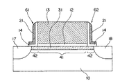
本発明の第1実施形態の図1に示す半導体記憶装置は、2ビットの記憶が可能な不揮発性メモリセルとして、図1に示すように、半導体基板10上に、第1の拡散層領域(ソース/ドレイン領域)17および第2の拡散層領域(ソース/ドレイン領域)18が形成されている。上記第1の拡散層領域17および第2の拡散層領域18を連結するようにチャネル形成領域31が形成されている。上記チャネル形成領域31上にゲート絶縁膜12が形成され、そのゲート絶縁膜12上に、通常のトランジスタと同程度のゲート長を有するゲート電極13が形成されている。また、上記ゲート絶縁膜12およびゲート電極13の両側の側壁に電荷保持体61,62が形成されている。さらに、第1,第2の拡散層領域(ソース/ドレイン領域)17,18は、ゲート電極13端部に対して(ゲート電極13が形成された領域41から)オフセットされている。
(First embodiment)
The semiconductor memory device shown in FIG. 1 according to the first embodiment of the present invention is a non-volatile memory cell capable of storing 2 bits, as shown in FIG. A source / drain region) 17 and a second diffusion layer region (source / drain region) 18 are formed. A
上記電荷保持体61,62、ゲート絶縁膜12およびゲート電極13で多値記憶体を構成している。
The
このように、半導体記憶装置の電荷保持体61,62は、ゲート絶縁膜12とは独立して形成されている。したがって、電荷保持体61,62が担うメモリ機能と、ゲート絶縁膜12が担うトランジスタ動作機能とは分離されている。また、ゲート電極13の両側に形成された2つの電荷保持体61,62は、ゲート電極13により分離されているので、書換え時の干渉が効果的に抑制される。したがって、この半導体記憶装置は、2ビットの記憶が可能で、かつ微細化が容易である。
As described above, the
また、第1,第2の拡散層領域(ソース/ドレイン領域)17,18がゲート電極13からオフセットされていることにより、ゲート電極13に電圧を印加したときの電荷保持体61,62下のオフセット領域42の反転しやすさを、電荷保持体61,62に蓄積された電荷量によって大きく変化させることができ、メモリ効果を増大させることが可能となる。更に、通常のロジックトランジスタと比較して、短チャネル効果を強力に防止することができ、より一層のゲート長の微細化を図ることができる。また、構造的に短チャネル効果抑制に適しているため、ロジックトランジスタと比較して膜厚の厚いゲート絶縁膜を採用することができ、信頼性を向上させることが可能となる。
In addition, since the first and second diffusion layer regions (source / drain regions) 17 and 18 are offset from the
また、チャネル形成領域31にカーボンナノチューブ(またはカーボンナノチューブと電子の移動度がシリコンの電子の移動度より高い半導体)を用いることにより、メモリの高速動作が可能になり、また、読み出し・書き込みおよび消去動作を繰り返し多数回行うことなどによってチャネルの移動度劣化が生じても、メモリ動作に必要な読み出し電流を保つことができ、長寿命で信頼性の高い安定したメモリ動作を得ることができる。
In addition, by using carbon nanotubes (or a semiconductor in which the mobility of electrons with respect to carbon nanotubes is higher than that of silicon electrons) in the
従来の半導体記憶装置では、読み出し・書き込みおよび消去のメモリ動作を10万回以上繰り返し行った場合、読み出し電流が保たれなくなっていき、消去後の読み出し電流値と書き込み後の電流値とが判別し難くなる現象が起こることあった。これに対して、半導体特性のカーボンナノチューブと、電子の移動度がシリコンの電子の移動度より高いシリコンゲルマニウム(SiGe)、インジウムリン(InP)、砒化ガリウム(GaAs)、ガリウムアンチモン(GaSb)、インジウムアンチモン(InSb)などの半導体を組み合わせた半導体膜をチャネル形成領域に用いることにより、メモリ動作を10万回以上繰り返し行った場合においてもメモリ動作に必要な読み出し電流が保たれているので書き込み後か消去後かの判別を容易に行うことが可能である。 In a conventional semiconductor memory device, when read / write and erase memory operations are repeated 100,000 times or more, the read current is not maintained, and the read current value after erase and the current value after write are discriminated. There was a phenomenon that became difficult. On the other hand, carbon nanotubes with semiconductor characteristics, and silicon germanium (SiGe), indium phosphide (InP), gallium arsenide (GaAs), gallium antimony (GaSb), indium whose electron mobility is higher than that of silicon. By using a semiconductor film in which a semiconductor such as antimony (InSb) is combined in the channel formation region, the read current necessary for the memory operation is maintained even after the memory operation is repeated 100,000 times or more. It is possible to easily determine whether it has been erased.
また、本発明の半導体記憶装置では、書き込み後か消去後かの判別が容易にできる電流差(書き込み後の読み出し電流と消去後の読み出し電流との電流差)を十分に保持していることから、大面積チップ上にメモリを作製したとき、面内において作製ばらつきが生じ、書き込み後・消去後の読み出し電流値のメモリ性能ばらつきが生じても、メモリ動作に必要な書き込み後と消去後の読み出し電流差を得ることができるので、歩留まりがよくなり、生産性の向上が可能となる。また、チャネル形成領域にカーボンナノチューブ(またはカーボンナノチューブと電子の移動度がシリコンの電子の移動度より高い半導体)を用いることにより、メモリの高速動作が可能になるので、従来の半導体記憶装置より低い電圧で従来の半導体記憶装置と同等の読み出し・書き込みおよび消去のメモリ動作を行うことができるので、省消費電力化が可能となる。 Further, in the semiconductor memory device of the present invention, the current difference (current difference between the read current after writing and the read current after erasing) that can easily determine whether it is after writing or after erasing is sufficiently retained. When memory is fabricated on a large-area chip, fabrication variations occur in-plane, and even if there is a variation in memory performance of read current values after writing and erasing, reading after writing and erasing necessary for memory operation Since a current difference can be obtained, yield is improved and productivity can be improved. In addition, the use of carbon nanotubes (or a semiconductor in which the mobility of carbon nanotubes and electrons is higher than that of silicon electrons) in the channel formation region enables high-speed operation of the memory, which is lower than conventional semiconductor memory devices. Since the read / write and erase memory operations equivalent to those of a conventional semiconductor memory device can be performed with a voltage, power consumption can be reduced.
本発明の半導体記憶装置の製造方法は、基板上全面にカーボンナノチューブを配置し、その上を酸化膜で被覆した後、通常のサイドウォール型のトランジスタと同じ方法で製造される。また、カーボンナノチューブ自身が最外層に絶縁層を有している場合は、その上を酸化膜で被覆しなくても良い。カーボンナノチューブを配置する方法は、作製されたカーボンナノチューブを精製し、アセトンなどの液体に混ぜ込んだ後、基板上に塗布する方法などがある。 In the method of manufacturing a semiconductor memory device of the present invention, carbon nanotubes are arranged on the entire surface of a substrate, and the carbon nanotube is covered with an oxide film, and then manufactured by the same method as that of a normal sidewall type transistor. Further, when the carbon nanotube itself has an insulating layer as the outermost layer, it is not necessary to cover it with an oxide film. As a method for arranging the carbon nanotubes, there is a method in which the produced carbon nanotubes are purified, mixed in a liquid such as acetone, and then applied onto a substrate.
また、サイドウォールスペーサ形状の電荷保持体61,62は、例えば図1に示すように、サイドウォール形状をしたシリコン窒化膜(または酸化アルミニウム膜)21とシリコン酸化膜14とからなる構造をしている。上記シリコン窒化膜(または酸化アルミニウム膜)21は、ゲート電極13、チャネル形成領域31および第1,第2の拡散層領域(ソース/ドレイン領域)17,18とシリコン酸化膜14により隔てられている。この電荷保持体61,62において電荷(電子または正孔)を蓄積する機能を有するのは、シリコン窒化膜(または酸化アルミニウム膜)21であり、シリコン窒化膜(または酸化アルミニウム膜)は、電荷をトラップする準位が多数存在するため、大きなヒステリシス特性を得ることができる。シリコン酸化膜14は、シリコン窒化膜(または酸化アルミニウム膜)21に蓄積された電荷の漏れを防いでいる。主として電荷を蓄積するのは、シリコン窒化膜(または酸化アルミニウム膜)21のうち、オフセット領域42上に存する部分である。
Further, the side wall spacer-shaped
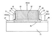
(第2実施形態)
本発明の第2実施形態の図2に示す半導体記憶装置は、電荷保持体を除いて第1実施形態の半導体記憶装置と同一の構成をしており、同一構成部は同一参照番号を付して説明を省略する。
(Second Embodiment)
The semiconductor memory device shown in FIG. 2 of the second embodiment of the present invention has the same configuration as that of the semiconductor memory device of the first embodiment except for the charge holding body, and the same components are denoted by the same reference numerals. The description is omitted.
図2に示すように、サイドウォールスペーサ形状の電荷保持体71,72は、シリコン窒化膜(または酸化アルミニウム膜)21がシリコン酸化膜14,16で挟まれた構造をしている。このように、電荷保持体71,72は、シリコン窒化膜(または酸化アルミニウム膜)21がシリコン酸化膜14,16によって挟まれているため、電荷保持体71,72に注入された電荷は、シリコン酸化膜16によりブロックされ、シリコン窒化膜(または酸化アルミニウム膜)21への電荷注入効率が上がり、書換え動作(書込みおよび消去動作)の高速化が実現し、信頼性の向上、十分な保持時間の確保が可能となる。シリコン窒化物、酸化アルミニウム、シリコン酸化物は、半導体装置の材料として用いられているものであるので、従来の半導体プロセスを用いて製造することができる。
As shown in FIG. 2, the side wall spacer-shaped
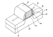
なお、図3は上記半導体記憶装置の斜視図であり、図3において31はカーボンナノチューブからなるチャネル形成領域を模式的に示している。
3 is a perspective view of the semiconductor memory device. In FIG. 3,
(第3実施形態)
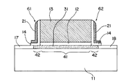
本発明の第3実施形態の図4に示す半導体記憶装置は、2ビットの記憶が可能な不揮発性メモリセルとして、図4に示したように、絶縁体基板11上に、第1の拡散層領域17(ソース/ドレイン領域)および第2の拡散層領域18(ソース/ドレイン領域)とチャネル形成領域31が形成されている。また、チャネル形成領域31上にゲート絶縁膜12が形成され、そのゲート絶縁膜12上に、通常のトランジスタと同程度のゲート長を有するゲート電極13が形成されている。また、ゲート絶縁膜12およびゲート電極13の両側の側壁に、電荷保持体61,62が形成されている。また、第1,第2の拡散層領域(ソース/ドレイン領域)17,18は、ゲート電極13端部に対して(ゲート電極13が形成された領域41から)オフセットされている。つまり、第1,第2実施形態の図1,図2に示したように半導体基板10上に構成されていたものを、図4では絶縁体基板11上に構成したものである。
(Third embodiment)
The semiconductor memory device shown in FIG. 4 according to the third embodiment of the present invention has a first diffusion layer on the
このように、絶縁体基板11上にチャネル形成領域31を設けることにより、完全素子分離ができ、また拡散層領域の容量が低減できるため、集積密度や動作速度の向上が可能である。また、半導体基板上にチャネル形成領域を形成する場合に比べ、リーク電流を抑制することができ、低消費電力化が可能である。また、従来のTFT(Thin Film Transistor:薄膜トランジスタ)のように絶縁体基板上に作製した半導体装置はチャネル形成領域にアモルファスシリコンやポリシリコンを用いているため、移動度が低いという問題があったが、チャネル形成領域にカーボンナノチューブ(またはカーボンナノチューブと電子の移動度がシリコンの電子の移動度より高い半導体)を用いることにより、高速動作が可能な半導体装置を大面積の絶縁体基板上に作製することが可能である。
Thus, by providing the
(第4実施形態)
本発明の第4実施形態の図5に示す半導体記憶装置は、電荷保持体を除いて第3実施形態の半導体記憶装置と同一の構成をしており、同一構成部は同一参照番号を付して説明を省略する。
(Fourth embodiment)
The semiconductor memory device shown in FIG. 5 of the fourth embodiment of the present invention has the same configuration as that of the semiconductor memory device of the third embodiment except for the charge holding body, and the same components are denoted by the same reference numerals. The description is omitted.
図5に示すように、サイドウォールスペーサ形状の電荷保持体71,72は、シリコン窒化膜(または酸化アルミニウム膜)21がシリコン酸化膜14,16で挟まれた構造を有している。
As shown in FIG. 5, the side wall spacer-shaped
上記構成の半導体記憶装置の動作原理について、図6A〜図8Bを用いて説明する。なお、図6A〜図8Bは、図5に示した電荷保持体を有する半導体記憶装置の場合を示しているが、その他の形状の電荷保持体を有する半導体記憶装置にも適用することができる。 The operation principle of the semiconductor memory device having the above structure will be described with reference to FIGS. 6A to 8B. 6A to 8B show the case of the semiconductor memory device having the charge holding body shown in FIG. 5, but the present invention can also be applied to a semiconductor memory device having charge carriers of other shapes.
なお、半導体記憶装置がNチャネル型の時は、チャネル形成領域31はP型、拡散層領域17,18はN型の導電型を有し、半導体記憶装置がPチャネル型のときはそれぞれ導電型が反対となる。以下の説明(読出し方法および消去方法に関する説明も含む)では、半導体記憶装置がNチャネル型の場合を説明するが、Pチャネル型の場合は電子と正孔の役割を逆にすればよい。また、Pチャネル型の場合は各ノードに印加する電圧の符号を全て反対にすればよい。
When the semiconductor memory device is an N-channel type, the
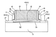
まず、この半導体記憶装置の第1の書込み方法について、図6A,図6Bを用いて説明する。なお、書込みとは、半導体記憶装置がNチャネル型のとき、電荷保持体に電子を注入することを指し、半導体記憶装置がPチャネル型のとき、電荷保持体に正孔を注入することを指すこととする。 First, a first writing method of the semiconductor memory device will be described with reference to FIGS. 6A and 6B. Note that writing refers to injecting electrons into the charge holding body when the semiconductor memory device is an N-channel type, and injecting holes into the charge holding body when the semiconductor memory device is a P-channel type. I will do it.
この半導体記憶装置の第1の書き込み方法は、ドレイン電界により加速された電子を電荷保持体71,72に注入することにより行う。
The first writing method of this semiconductor memory device is performed by injecting electrons accelerated by the drain electric field into the
第2の電荷保持体72に電子を注入する(書込む)ためには、図6Aに示すように、第1の拡散層領域17をソース電極に、第2の拡散層領域18をドレイン電極とする。例えば、第1の拡散層領域17に0V、第2の拡散層領域18に+5V、ゲート電極13に+5Vを印加すればよい。このような電圧条件によれば、反転層32が、第1の拡散層領域17(ソース電極)から伸びるが、第2の拡散層領域18(ドレイン電極)に達することなく、ピンチオフ点が発生する。電子は、ピンチオフ点から第2の拡散層領域18(ドレイン電極)までドレイン電界により加速され、第2の電荷保持体72(より正確には第2の電荷保持体72内のシリコン窒化膜(または酸化アルミニウム膜)21)に注入されて、書込みが行なわれる。なお、第1の電荷保持体71近傍では、ドレイン電界により加速された電子が発生しないため、書込みは行なわれない。なお、書込み動作のための電圧は上記に限らず、例えば、第1の拡散層領域17に0V、第2の拡散層領域18に+10V、ゲート電極13に+5Vを印加した場合も、第2の電荷保持体72にホットエレクトロン(熱電子)が注入されて書込みが行なわれた。
In order to inject (write) electrons into the second
このようにして、第2の電荷保持体72に電子を注入して、書込みを行なうことができる。
In this way, writing can be performed by injecting electrons into the second
一方、第1の電荷保持体71に電子を注入する(書込む)ためには、図6Bに示すように、第2の拡散層領域18をソース電極に、第1の拡散層領域17をドレイン電極とする。例えば、第2の拡散層領域18に0V、第1の拡散層領域17に+5V、ゲート電極13に+5Vを印加すればよい。このように、第2の電荷保持体72に電子を注入する場合は、第1,第2の拡散層領域(ソース/ドレイン領域)17,18を入れ替えることにより、第1の電荷保持体71に電子を注入して、書込みを行なうことができる。
On the other hand, in order to inject (write) electrons into the
次に、この半導体記憶装置の第2の書込み方法について、図7A,図7Bを用いて説明する。 Next, a second writing method of the semiconductor memory device will be described with reference to FIGS. 7A and 7B.
この第2の書込み方法によって、第2の電荷保持体72に電子を注入する(書込む)ためには、図7Aに示すように、第1の拡散層領域17をソース電極に、第2の拡散層領域18をドレイン電極とする。この第2の書込み方法に特有な点は、第1の拡散層領域17の電位よりも、チャネル形成領域31の電位を低くすることである。例えば、第1の拡散層領域17に2V、第2の拡散層領域18に+5V、ゲート電極13に+5Vを印加すればよい。すなわち、一方のN型拡散層領域(第1の拡散層領域17)を基準電圧とし、他方のN型拡散層領域(第2の拡散層領域18)を基準電圧より高い電圧とし、ゲート電極13を基準電圧より高い電圧とし、P型チャネル形成領域(チャネル形成領域11)を基準電圧より低い電圧とする。なお、各ノードに与える電位は上記の限りではなく、その最適値は半導体記憶装置の構造などに依存する。また、ゲート電極13および第2の拡散層領域18の電位は、それぞれ第1の拡散層領域17の電位より高くなくてはならないが、ゲート電極13の電位と第2の拡散層領域18の電位との大小関係は問われない。
In order to inject (write) electrons into the second
この第2の書込み方法は、第1の書込み方法に比べて非常に少ない電流で書込みが行なわれる。言い換えれば、第2の書込み方法における電荷注入効率は、第1の書込方法に比べてはるかに高くなっている。 In the second writing method, writing is performed with a very small current compared to the first writing method. In other words, the charge injection efficiency in the second writing method is much higher than that in the first writing method.
一方、第1の電荷保持体71に電子を注入する(書込む)ためには、図7Bに示すように、第2の拡散層領域18をソース電極に、第1の拡散層領域17をドレイン電極とする。例えば、第2の拡散層領域18に2V、第1の拡散層領域17に+5V、ゲート電極13に+5Vを印加すればよい。このように、第2の電荷保持体72に電子を注入する場合とは、第1,第2の拡散層領域(ソース/ドレイン領域)17,18を入れ替えることにより、第1の電荷保持体71に電子を注入して、書込みを行なうことができる。
On the other hand, in order to inject (write) electrons into the first
上記第2の書込み方法によれば、非常に高い効率で所望の電荷保持体に選択的に電子注入を行なうことができる。したがって、書込み電流値を大幅に低くして、半導体記憶装置の消費電力を削減することができる。 According to the second writing method, electrons can be selectively injected into a desired charge holding body with very high efficiency. Therefore, the write current value can be significantly reduced, and the power consumption of the semiconductor memory device can be reduced.
次に、上記半導体記憶装置の読み出し動作原理を説明する(図示せず)。 Next, the principle of read operation of the semiconductor memory device will be described (not shown).
上記第1の電荷保持体71に記憶された情報を読み出す場合、第1の拡散層領域17をソース電極に、第2の拡散層領域18をドレイン電極とし、トランジスタを飽和領域動作させる。例えば、第1の拡散層領域17に0V、第2の拡散層領域18に+2V、ゲート電極13に+3Vを印加すればよい。このとき、第1の電荷保持体71に電子が蓄積していない場合には、ドレイン電流が流れやすい。一方、第1の電荷保持体71に電子が蓄積している場合は、第1の電荷保持体71近傍で反転層が形成されにくいので、ドレイン電流は流れにくい。したがって、ドレイン電流を検出することにより、第1の電荷保持体71の記憶情報を読み出すことができる。このとき、第2の電荷保持体72における電荷蓄積の有無は、ドレイン近傍がピンチオフしているため、ドレイン電流に影響を与えない。
When reading the information stored in the first
一方、第2の電荷保持体72に記憶された情報を読み出す場合、第2の拡散層領域18をソース電極に、第1の拡散層領域17をドレイン電極とし、トランジスタを飽和領域動作させる。例えば、第2の拡散層領域18に0V、第1の拡散層領域17に+2V、ゲート電極13に+3Vを印加すればよい。このように、第1の電荷保持体71に記憶された情報を読み出す場合とは、第1,第2の拡散層領域(ソース/ドレイン領域)17,18を入れ替えることにより、第2の電荷保持体72に記憶された情報の読出しを行なうことができる。
On the other hand, when information stored in the second
なお、ゲート電極13で覆われないチャネル形成領域(オフセット領域42)においては、電荷保持体71,72の余剰電子の有無によって反転層が消失または形成され、その結果、大きなヒステリシス(閾値の変化)が得られる。ただし、オフセット領域42の幅があまり大きいと、ドレイン電流が大きく減少し、読出し速度が大幅に遅くなる。したがって、十分なヒステリシスと読出し速度が得られるように、オフセット領域42の幅を決定することが好ましい。
In the channel formation region (offset region 42) that is not covered by the
また、上記第1,第2の拡散層領域17,18がゲート電極13端に達している場合、つまり、第1,第2の拡散層領域17,18とゲート電極13とがオーバーラップしている場合であっても、書き込み動作によりトランジスタの閾値はほとんど変わらなかったが、ソース/ドレイン端での寄生抵抗が大きく変わり、ドレイン電流は大きく減少(1桁以上)した。したがって、ドレイン電流の検出により読出しが可能であり、メモリとしての機能を得ることができる。
Further, when the first and second
次に、上記半導体記憶装置の消去方法を図8A,図8Bで説明する。 Next, an erasing method of the semiconductor memory device will be described with reference to FIGS. 8A and 8B.
まず、第2の電荷保持体72に記憶された情報を消去する場合、図8Aに示すように第2の拡散層領域18に正電圧(例えば、+5V)を印加して、第2の拡散層領域18とチャネル形成領域31とのPN接合に逆バイアスをかけ、更にゲート電極13に負電圧(例えば、−5V)を印加すればよい。このとき、上記PN接合のうちゲート電極13付近では、負電圧が印加されたゲート電極13の影響により、特にポテンシャルの勾配が急になる。そのため、バンド間トンネルによりPN接合のチャネル形成領域31側にホール(正孔)が発生する。このホールが負の電位をもつゲート電極13方向に引きこまれ、その結果、第2の電荷保持体72にホールが注入される。このようにして、第2の電荷保持体72の消去が行なわれる。このとき第1の拡散層領域17には0Vを印加すればよい。
First, when erasing information stored in the second
上記第1の消去方法において、第1の電荷保持体71に記憶された情報を消去する場合は、上記において第1の拡散層領域17と第2の拡散層領域18の電位を入れ替えればよい(図8B)。
In the first erasing method, when the information stored in the first
上記動作方法では、ソース電極とドレイン電極を入れ替えることによって1トランジスタ当り2ビットの書込みおよび消去をさせているが、ソース電極とドレイン電極を固定して1ビットメモリとして動作させてもよい。この場合、第1,第2の拡散層領域(ソース/ドレイン領域)の一方を共通固定電圧とすることが可能となり、第1,第2の拡散層領域(ソース/ドレイン領域)に接続されるビット線の本数を半減できる。 In the above operation method, writing and erasing of 2 bits per transistor are performed by switching the source electrode and the drain electrode. However, the source electrode and the drain electrode may be fixed and operated as a 1-bit memory. In this case, one of the first and second diffusion layer regions (source / drain regions) can be set to a common fixed voltage, and is connected to the first and second diffusion layer regions (source / drain regions). The number of bit lines can be halved.
上記第1〜第4実施形態の半導体記憶装置によれば、電荷保持体は、ゲート絶縁膜とは独立してゲート電極の両側に形成され、2ビット動作が可能である。更には、各電荷保持体はゲート電極により分離されているので、書換え時の干渉が効果的に抑制される。また、電荷保持体が担うメモリ機能と、ゲート絶縁膜が担うトランジスタ動作機能とは分離されているので、ゲート絶縁膜を薄膜化して短チャネル効果を抑制することができる。したがって、素子の微細化が容易となる。 According to the semiconductor memory devices of the first to fourth embodiments, the charge holding body is formed on both sides of the gate electrode independently of the gate insulating film, and a 2-bit operation is possible. Furthermore, since each charge holding body is separated by the gate electrode, interference during rewriting is effectively suppressed. In addition, since the memory function of the charge holding body and the transistor operation function of the gate insulating film are separated, the gate insulating film can be thinned to suppress the short channel effect. Therefore, the element can be easily miniaturized.
また、この半導体記憶装置の第2の書込み方法によれば、電荷保持体に電子を高い効率で注入することができる。したがって、書込み電流値を大幅に低くして、半導体記憶装置の消費電力を削減することができる。 Further, according to the second writing method of the semiconductor memory device, electrons can be injected into the charge holding body with high efficiency. Therefore, the write current value can be significantly reduced, and the power consumption of the semiconductor memory device can be reduced.
本発明の半導体記憶装置は、主として、複数の電荷保持体を有する多値記憶体と、上記多値記憶体の上記電荷保持体に夫々対応する拡散層領域と、上記多値記憶体の下側に配置され、上記拡散層領域を連結するチャネル形成領域とから構成される。この半導体記憶装置は、1つの電荷保持体に2値またはそれ以上の情報を記憶することにより、4値またはそれ以上の情報を記憶するメモリ素子として機能する。 The semiconductor memory device according to the present invention mainly includes a multi-value memory having a plurality of charge carriers, a diffusion layer region corresponding to each of the charge carriers of the multi-value memory, and a lower side of the multi-value memory. And a channel forming region connecting the diffusion layer regions. This semiconductor memory device functions as a memory element for storing quaternary or higher information by storing binary or higher information in one charge holding body.
上記チャネル形成領域は、カーボンナノチューブを含む膜であるか、またはカーボンナノチューブと電子の移動度がシリコンの電子の移動度より高い半導体を含む膜である。上記電子の移動度がシリコンの電子の移動度より高い半導体としては、例えば、シリコンゲルマニウム(SiGe)、インジウムリン(InP)、砒化ガリウム(GaAs)、ガリウムアンチモン(GaSb)、インジウムアンチモン(InSb)などがある。 The channel formation region is a film containing carbon nanotubes or a film containing a semiconductor in which the mobility of carbon nanotubes and electrons is higher than the mobility of electrons of silicon. Examples of semiconductors having higher electron mobility than silicon electron mobility include silicon germanium (SiGe), indium phosphide (InP), gallium arsenide (GaAs), gallium antimony (GaSb), and indium antimony (InSb). There is.
カーボンナノチューブは、炭素の同素体であり、各炭素原子が6角形の各頂点に配置され結合して形成されたグラフェンのシート状のものがナノサイズの直径で丸く巻かれた形をなしている。カーボンナノチューブは、電気伝導度、熱伝導度が高く、物理的、化学的に強靭であり、また、カーボンナノチューブはグラフェンの巻かれる角度および構造によって金属または半導体の特性を示す。カーボンナノチューブは、その電気的な性質によって相異なる2種のカーボンナノチューブに分けられる。すなわち、ゲート電圧に関係なく、電流電圧特性が線形関係を示す金属性カーボンナノチューブと、ゲート電圧に大きく影響され、電流電圧特性が非線形関係を示す半導体特性(バンドギャップの大きいものは絶縁体に近似)のカーボンナノチューブとに分けられる。 A carbon nanotube is an allotrope of carbon, and has a shape in which a sheet of graphene formed by arranging and bonding each carbon atom at each vertex of a hexagon is rounded with a nano-sized diameter. Carbon nanotubes have high electrical and thermal conductivity, are physically and chemically tough, and carbon nanotubes exhibit metal or semiconductor characteristics depending on the angle and structure of graphene. Carbon nanotubes are divided into two types of carbon nanotubes that differ from each other depending on their electrical properties. That is, metallic carbon nanotubes whose current-voltage characteristics are linearly related regardless of the gate voltage, and semiconductor characteristics whose current-voltage characteristics are non-linearly influenced greatly by the gate voltage (those with a large band gap approximate to an insulator) ) Carbon nanotubes.
本発明の実施形態に係る半導体記憶装置に用いられるカーボンナノチューブは、半導体特性のカーボンナノチューブであって、ゲート電極に印加される電圧によってカーボンナノチューブを通じて移動する電子の流れ、すなわち電流が制御される。このようなカーボンナノチューブは、電気放電法、レーザー蒸着法、プラズマ化学気相蒸着法、熱化学気相蒸着法、気相合成法などを用いて作製することができる。 The carbon nanotube used in the semiconductor memory device according to the embodiment of the present invention is a carbon nanotube having semiconductor characteristics, and the flow of electrons moving through the carbon nanotube, that is, the current is controlled by the voltage applied to the gate electrode. Such carbon nanotubes can be produced using an electric discharge method, a laser vapor deposition method, a plasma chemical vapor deposition method, a thermal chemical vapor deposition method, a vapor phase synthesis method, or the like.
また、チャネル形成領域に、電子の移動度がシリコンの電子の移動度1880[cm2/V・s]より高い半導体を用いることにより、半導体記憶装置の読み出し・書き込みおよび消去のメモリ動作の高速化が可能となり、また、多数回のメモリ動作を繰り返し行うことでチャネルの移動度劣化が生じても、メモリ動作に必要な読み出し電流を保つことができ、長寿命で信頼性の高い安定したメモリ動作を得ることができる。 Further, by using a semiconductor whose electron mobility is higher than the electron mobility 1880 [cm 2 / V · s] of silicon for the channel formation region, the memory operation for reading / writing and erasing of the semiconductor memory device can be accelerated. In addition, it is possible to maintain the read current necessary for memory operation even when channel mobility is deteriorated by repeatedly performing memory operations many times. Can be obtained.
このように、電気伝導度、熱伝導度の高いカーボンナノチューブをチャネル形成領域に用いることにより、半導体記憶装置の小型化による抵抗の増加がなく熱損失、電力消耗、電気的特性変動、電荷漏れが少なく、素子の微細化(高集積化)が図れると共に、信頼性の高い安定したメモリ動作を得ることができる。 Thus, by using carbon nanotubes with high electrical conductivity and thermal conductivity in the channel formation region, there is no increase in resistance due to downsizing of the semiconductor memory device, and heat loss, power consumption, electrical characteristic fluctuations, and charge leakage are eliminated. Thus, the device can be miniaturized (highly integrated), and a highly reliable and stable memory operation can be obtained.
また、カーボンナノチューブ内を流れる電流は、ほとんど抵抗なく流れるので、上記電荷保持体に保持された電荷の影響を強く表すことになり、電荷の有無の判別を容易に行うことができ、多値の不揮発性メモリに適している。 In addition, since the current flowing through the carbon nanotube flows almost without resistance, the influence of the charge held in the charge holding body is strongly expressed, and the presence / absence of the charge can be easily determined. Suitable for non-volatile memory.
また、書き込み後か消去後かの判別が容易にできるだけの電流差(書き込み後と消去後の読み出し電流の差)を十分に保持していることから、大面積チップ上にメモリを作製したとき、面内において作製ばらつきが生じ、書き込み後・消去後の読み出し電流値のメモリ性能ばらつきが生じても、メモリ動作に必要な書き込み後と消去後の読み出し電流差を得ることができるので、歩留まりをよくすることができ、生産性を向上させることができる。 In addition, since the current difference (difference between read current after write and erase) is sufficiently retained to easily determine whether it is after writing or after erasing, when creating a memory on a large area chip, Even if manufacturing variations occur in-plane and memory performance varies after reading and erasing, the difference in reading current after writing and erasing necessary for memory operation can be obtained, so the yield is improved. Productivity can be improved.
本発明の半導体記憶装置は、第1,第2実施形態のように半導体基板上、好ましくは半導体基板内に形成された第1導電型のウェル領域上、あるいは第3,第4実施形態のように絶縁体基板上に形成されることが好ましい。 The semiconductor memory device of the present invention is on a semiconductor substrate as in the first and second embodiments, preferably on a first conductivity type well region formed in the semiconductor substrate, or as in the third and fourth embodiments. It is preferably formed on an insulator substrate.
半導体基板としては、半導体装置に使用されるものであれば特に限定されるものではなく、例えば、シリコン、ゲルマニウム等の元素半導体、GaAs、InGaAs、ZnSe等の化合物半導体による基板、SOI基板または多層SOI基板等の種々の基板を用いることができる。なかでもシリコン基板または表面半導体層としてシリコン層が形成されたSOI基板が好ましい。この半導体基板上には、素子分離領域が形成されていることが好ましく、更にトランジスタ、キャパシタ、抵抗等の素子、これらによる回路、半導体装置や層間絶縁膜が組み合わせられて、シングルまたはマルチレイヤー構造で形成されていてもよい。なお、素子分離領域は、LOCOS(Local Oxidation Of Silicon:局所酸化シリコン)膜、トレンチ酸化膜、STI(Shallow Trench Isolation;浅い溝分離法)膜等種々の素子分離膜により形成することができる。さらに、半導体基板は、P型またはN型の導電型を有していてもよく、半導体基板には、少なくとも1つの第1導電型(P型またはN型)のウェル領域が形成されていることが好ましい。半導体基板およびウェル領域の不純物濃度は、当該分野で公知の範囲のものが使用できる。なお、半導体基板としてSOI(Silicon on Insulator: シリコン・オン・インシュレータ)基板を用いる場合には、表面半導体層には、ウェル領域が形成されていてもよいが、チャネル形成領域下にボディ領域を有していてもよい。 The semiconductor substrate is not particularly limited as long as it is used in a semiconductor device. For example, an elemental semiconductor such as silicon or germanium, a compound semiconductor such as GaAs, InGaAs, or ZnSe, an SOI substrate, or a multilayer SOI. Various substrates such as a substrate can be used. Among these, a silicon substrate or an SOI substrate on which a silicon layer is formed as a surface semiconductor layer is preferable. An element isolation region is preferably formed on this semiconductor substrate, and further, elements such as transistors, capacitors, resistors, etc., circuits using these elements, semiconductor devices, and interlayer insulating films are combined to form a single or multi-layer structure. It may be formed. The element isolation region can be formed by various element isolation films such as a LOCOS (Local Oxidation Of Silicon) film, a trench oxide film, and an STI (Shallow Trench Isolation) film. Furthermore, the semiconductor substrate may have a P-type or N-type conductivity type, and at least one first conductivity type (P-type or N-type) well region is formed in the semiconductor substrate. Is preferred. The impurity concentration in the semiconductor substrate and the well region can be within the range known in the art. When an SOI (Silicon on Insulator) substrate is used as the semiconductor substrate, a well region may be formed in the surface semiconductor layer, but a body region is provided under the channel formation region. You may do it.
絶縁体または酸化膜としては、通常、半導体装置に使用されるものであれば特に限定されるものではなく、例えば、シリコン酸化膜、シリコン窒化膜、等の絶縁膜:酸化アルミニウム膜、酸化チタニウム膜、酸化タンタル膜、酸化ハフニウム膜などの高誘電体膜の単層膜または積層膜、カーボンナノチューブ絶縁層などを使用することができる。なかでも、シリコン酸化膜が好ましい。 The insulator or oxide film is not particularly limited as long as it is usually used in a semiconductor device. For example, an insulating film such as a silicon oxide film or a silicon nitride film: an aluminum oxide film, a titanium oxide film, or the like. A single-layer film or a laminated film of a high dielectric film such as a tantalum oxide film or a hafnium oxide film, a carbon nanotube insulating layer, or the like can be used. Of these, a silicon oxide film is preferable.
また、本発明の半導体記憶装置のゲート電極は、ゲート絶縁膜上に、通常半導体装置に使用されるような形状で形成されている。このゲート電極は、実施の形態のなかで特に指定がない限り、特に限定されるものではなく、導電膜、例えば、ポリシリコン、銅・アルミニウム等の金属、タングステン・チタン・タンタル等の高融点金属、高融点金属とのシリサイド等の単層膜または積層膜等が挙げられる。ゲート電極の膜厚は、例えば10nm〜400nm程度の膜厚で形成することが適当である。 In addition, the gate electrode of the semiconductor memory device of the present invention is formed on the gate insulating film in a shape normally used for a semiconductor device. The gate electrode is not particularly limited unless otherwise specified in the embodiment, and a conductive film, for example, a metal such as polysilicon, copper or aluminum, or a refractory metal such as tungsten, titanium or tantalum. In addition, a single layer film or a laminated film such as silicide with a refractory metal can be used. The gate electrode is suitably formed to a thickness of about 10 nm to 400 nm, for example.
また、本発明の半導体記憶装置のチャネル形成領域は、ゲート電極の下に形成されるが、ゲート電極下のみならず、ゲート電極とゲート長方向におけるゲート端の外側を含む領域下に形成されている。このように、ゲート電極で覆われていないチャネル形成領域が存在する場合には、そのチャネル形成領域は、ゲート絶縁膜または後述する電荷保持体で覆われていることが好ましい。 The channel formation region of the semiconductor memory device of the present invention is formed under the gate electrode, but not only under the gate electrode but also under the region including the gate electrode and the outside of the gate end in the gate length direction. Yes. As described above, when there is a channel formation region that is not covered with the gate electrode, the channel formation region is preferably covered with a gate insulating film or a charge holding body described later.
また、本発明の半導体記憶装置の電荷保持体は、直接または絶縁膜を介してゲート電極の両側に形成されており、また、直接、ゲート絶縁膜または絶縁膜を介して基板(チャネル形成領域、第1,第2の拡散層領域(ソース/ドレイン領域))上に配置している。ゲート電極の両側の電荷保持体は、直接または絶縁膜を介してゲート電極の側壁の全てを覆うように形成されていてもよいし、一部を覆うように形成されてもよい。電荷保持体として導電膜を用いる場合には、電荷保持体が基板(チャネル形成領域、第1,第2の拡散層領域(ソース/ドレイン領域))またはゲート電極と直接接触しないように、絶縁膜を介して配置させることが好ましい。例えば、導電膜と絶縁膜との積層構造、絶縁膜内に導電膜をドット状等に分散させた構造、ゲートの側壁に形成された側壁絶縁膜内の一部に配置した構造等が挙げられる。 Further, the charge holding body of the semiconductor memory device of the present invention is formed on both sides of the gate electrode directly or via an insulating film, and directly on the substrate (channel forming region, via the gate insulating film or insulating film). First and second diffusion layer regions (source / drain regions)). The charge holding bodies on both sides of the gate electrode may be formed so as to cover all of the side walls of the gate electrode directly or via an insulating film, or may be formed so as to cover a part thereof. When a conductive film is used as the charge holding body, an insulating film is used so that the charge holding body does not come into direct contact with the substrate (channel formation region, first and second diffusion layer regions (source / drain region)) or the gate electrode. It is preferable to arrange via. For example, a laminated structure of a conductive film and an insulating film, a structure in which a conductive film is dispersed in a dot shape or the like in the insulating film, a structure in which the conductive film is disposed in a part of the side wall insulating film formed on the side wall of the gate, etc. .
上記電荷保持体は、電荷を蓄積する第1の絶縁体からなる膜が、第2の絶縁体からなる膜と第3の絶縁体からなる膜とで挟まれたサンドウィッチ構造を有するのが好ましい。電荷を蓄積する第1の絶縁体が膜状であるから、電荷の注入により短い時間で第1の絶縁体内の電荷密度を上げ、また、電荷密度を均一にすることができる。電荷を蓄積する第1の絶縁体内の電荷分布が不均一であった場合、保持中に第1の絶縁体内を電荷が移動して信頼性が低下する恐れがある。また、電荷を蓄積する第1の絶縁体は、導電体部(ゲート電極、拡散層領域、チャネル形成領域)とは他の絶縁膜で隔てられているので、電荷の漏れが抑制されて十分な保持時間を得ることができる。したがって、上記サンドウィッチ構造を有する場合、半導体記憶装置の高速書換え、信頼性の向上、十分な保持時間の確保が可能となる。上記条件を満たす電荷保持体としては、上記第1の絶縁体をシリコン窒化膜(または酸化アルミニウム膜)とし、第2および第3の絶縁体をシリコン酸化膜とするのが特に好ましい。シリコン窒化膜(または酸化アルミニウム膜)は、電荷をトラップする準位が多数存在するため、大きなヒステリシス特性を得ることができる。また、シリコン酸化膜およびシリコン窒化膜は共に半導体プロセスでごく標準的に用いられる材料であるため、好ましい。なお、上記第2および第3の絶縁体は、異なる物質であってもよいし同一の物質であってもよい。 The charge holding body preferably has a sandwich structure in which a film made of a first insulator for accumulating charges is sandwiched between a film made of a second insulator and a film made of a third insulator. Since the first insulator for accumulating charges is in the form of a film, the charge density in the first insulator can be increased and the charge density can be made uniform in a short time by the injection of charges. If the charge distribution in the first insulator that accumulates the charge is non-uniform, the charge may move through the first insulator during holding, and reliability may be reduced. Further, since the first insulator for accumulating charges is separated from the conductor portion (gate electrode, diffusion layer region, channel formation region) by another insulating film, leakage of charges is suppressed and sufficient. Retention time can be obtained. Therefore, in the case of having the sandwich structure, it is possible to rewrite the semiconductor memory device at high speed, improve reliability, and ensure a sufficient holding time. As the charge holding body satisfying the above conditions, it is particularly preferable that the first insulator is a silicon nitride film (or aluminum oxide film) and the second and third insulators are silicon oxide films. Since the silicon nitride film (or aluminum oxide film) has many levels for trapping charges, a large hysteresis characteristic can be obtained. In addition, both the silicon oxide film and the silicon nitride film are preferable because they are materials that are extremely used in a semiconductor process. The second and third insulators may be different materials or the same material.
また、本発明の半導体記憶装置の第1,第2の拡散層領域(ソース/ドレイン領域)は、半導体基板(またはウェル領域)と逆導電型の拡散層領域として、電荷保持体のゲート電極の両側のそれぞれに配置されている。上記第1,第2の拡散層領域(ソース/ドレイン領域)と半導体基板(またはウェル領域)との接合は、不純物濃度が急峻であることが好ましい。ホットエレクトロンやホットホールが低電圧で効率良く発生し、より低電圧で高速な動作が可能となるからである。上記第1,第2の拡散層領域(ソース/ドレイン領域)の接合深さは、特に限定されるものではなく、得ようとする半導体記憶装置の性能等に応じて、適宜調整することができる。なお、半導体基板としてSOI基板を用いる場合には、第1,第2の拡散層領域(ソース/ドレイン領域)は、表面半導体層の膜厚よりも小さな接合深さを有していてもよいが、表面半導体層の膜厚とほぼ同程度の接合深さを有していることが好ましい。 In addition, the first and second diffusion layer regions (source / drain regions) of the semiconductor memory device of the present invention serve as diffusion layer regions having a conductivity type opposite to that of the semiconductor substrate (or well region). Located on each side. The junction between the first and second diffusion layer regions (source / drain regions) and the semiconductor substrate (or well region) preferably has a steep impurity concentration. This is because hot electrons and hot holes are efficiently generated at a low voltage, and a high-speed operation can be performed at a lower voltage. The junction depths of the first and second diffusion layer regions (source / drain regions) are not particularly limited, and can be appropriately adjusted according to the performance of the semiconductor memory device to be obtained. . When an SOI substrate is used as the semiconductor substrate, the first and second diffusion layer regions (source / drain regions) may have a junction depth smaller than the film thickness of the surface semiconductor layer. It is preferable that the junction depth is approximately the same as the film thickness of the surface semiconductor layer.
上記第1,第2の拡散層領域(ソース/ドレイン領域)は、ゲート電極端とオーバーラップするように配置していてもよいし、ゲート電極端と一致するように配置してもよいし、ゲート電極端に対してオフセットされて配置されていてもよい。特に、オフセットされている場合には、ゲート電極に電圧を印加したとき、電荷保持体下のオフセット領域の反転しやすさが、電荷保持体に蓄積された電荷量によって大きく変化し、メモリ効果が増大するとともに、短チャネル効果の低減をもたらすため、好ましい。ただし、あまりオフセットし過ぎると、ソース・ドレイン間の駆動電流が著しく小さくなるため、ゲート長方向に対して平行方向の電荷保持体の厚さよりもオフセット量つまり、ゲート長方向における一方のゲート電極端から近い方のソース・ドレイン領域までの距離は短い方が好ましい。特に重要なことは、電荷保持体中の電荷蓄積領域の少なくとも一部が、第1,第2の拡散層領域である第1,第2の拡散層領域(ソース/ドレイン領域)の一部とオーバーラップしていることである。本発明の半導体記憶装置の本質は、電荷保持体の側壁部にのみ存在するゲート電極と第1,第2の拡散層領域(ソース/ドレイン領域)間の電圧差により電荷保持体を横切る電界によって記憶を書き換えることであるためである。 The first and second diffusion layer regions (source / drain regions) may be disposed so as to overlap the gate electrode end, may be disposed so as to coincide with the gate electrode end, It may be arranged offset with respect to the gate electrode end. In particular, when offset is applied, when a voltage is applied to the gate electrode, the ease of inversion of the offset region under the charge holding body greatly varies depending on the amount of charge accumulated in the charge holding body, and the memory effect is improved. This is preferred because it increases and leads to a reduction in the short channel effect. However, if the offset is too much, the drive current between the source and the drain becomes extremely small. Therefore, the offset amount is larger than the thickness of the charge holding member in the direction parallel to the gate length direction, that is, one gate electrode end in the gate length direction. It is preferable that the distance from the source to the nearer source / drain region is shorter. Of particular importance is that at least a portion of the charge storage region in the charge carrier is a portion of the first and second diffusion layer regions (source / drain regions) that are the first and second diffusion layer regions. It is overlapping. The essence of the semiconductor memory device of the present invention is that an electric field across the charge holding body is caused by a voltage difference between the gate electrode existing only on the side wall portion of the charge holding body and the first and second diffusion layer regions (source / drain regions). This is because the memory is rewritten.
また、上記第1,第2の拡散層領域(ソース/ドレイン領域)は、その一部が、ゲート絶縁膜下面よりも高い位置に延設されていてもよい。この場合には、半導体基板内に形成された第1,第2の拡散層領域上に、この第1,第2の拡散層領域と一体化した導電膜が積層されて構成されていることが適当である。導電膜としては、例えば、ポリシリコン、アモルファスシリコン等の半導体、シリサイド、上述した金属、高融点金属等が挙げられる。なかでも、ポリシリコンが好ましい。ポリシリコンは、不純物拡散速度が半導体基板に比べて非常に大きいために、半導体基板内における第1,第2の拡散層領域の接合深さを浅くするのが容易で、短チャネル効果の抑制がしやすいためである。なお、この場合には、この第1,第2の拡散層領域の一部は、ゲート電極とともに、電荷保持体の少なくとも一部を挟持するように配置することが好ましい。 In addition, a part of the first and second diffusion layer regions (source / drain regions) may be extended to a position higher than the lower surface of the gate insulating film. In this case, the conductive film integrated with the first and second diffusion layer regions is laminated on the first and second diffusion layer regions formed in the semiconductor substrate. Is appropriate. Examples of the conductive film include semiconductors such as polysilicon and amorphous silicon, silicide, the above-described metals, refractory metals, and the like. Of these, polysilicon is preferable. Since polysilicon has a very high impurity diffusion rate compared to a semiconductor substrate, it is easy to reduce the junction depth of the first and second diffusion layer regions in the semiconductor substrate and suppress the short channel effect. It is because it is easy to do. In this case, it is preferable that a part of the first and second diffusion layer regions is arranged so as to sandwich at least a part of the charge holding body together with the gate electrode.
本発明の半導体記憶装置は、ゲート絶縁膜上に形成された単一のゲート電極、ソース領域、ドレイン領域および半導体基板を4個の端子として、この4個の端子のそれぞれに所定の電位を与えることにより、書込み、消去、読出しの各動作を行なう。したがって、本発明の半導体記憶装置をアレイ状に配置してメモリセルアレイを構成した場合、単一の制御ゲートで各メモリセルを制御できるので、ワード線の本数を少なくすることができる。 The semiconductor memory device of the present invention uses a single gate electrode, a source region, a drain region, and a semiconductor substrate formed on a gate insulating film as four terminals, and applies a predetermined potential to each of the four terminals. Thus, write, erase, and read operations are performed. Therefore, when the memory cell array is configured by arranging the semiconductor memory devices of the present invention in an array, each memory cell can be controlled by a single control gate, so that the number of word lines can be reduced.
本発明の半導体記憶装置は、チャネル形成領域に、半導体特性のカーボンナノチューブを用いることにより、メモリの高速動作が可能になり、また、読み出し・書き込みおよび消去のメモリ動作を繰り返し多数回行うことなどによってチャネルの移動度劣化が生じても、メモリ動作に必要な読み出し電流を保つことができ、長寿命で信頼性の高い安定したメモリ動作を得ることができる。例えば、読み出し・書き込みおよび消去のメモリ動作を10万回以上繰り返し行っても、読み出し電流が保たれているので書き込み後か消去後かの判別を容易に行うことができる。 In the semiconductor memory device of the present invention, the use of carbon nanotubes having semiconductor characteristics in the channel formation region enables high-speed operation of the memory, and by repeatedly performing read / write and erase memory operations many times. Even when channel mobility is deteriorated, a read current necessary for memory operation can be maintained, and a stable memory operation with a long lifetime and high reliability can be obtained. For example, even if the read / write and erase memory operations are repeated 100,000 times or more, the read current is maintained, so that it is possible to easily determine whether the data has been written or erased.
また、本発明の半導体記憶装置は、電池駆動の携帯電子機器、特に携帯情報端末に用いることができる。携帯電子機器としては、携帯情報端末、携帯電話、ゲーム機器等が挙げられる。 The semiconductor memory device of the present invention can be used for a battery-driven portable electronic device, particularly a portable information terminal. Examples of the portable electronic device include a portable information terminal, a mobile phone, and a game device.
なお、電荷保持体の構造は、上記第1〜第4実施形態の半導体記憶装置に限らず、例えば、電荷保持体に電荷を蓄積する機能を有する量子ドットが含まれているものでもよい。また、電荷保持体の形状はサイドウォール形状を有している必要はなく、ゲート電極の両側にあって、その一部が半導体基板および第1,第2の拡散層領域(ソース/ドレイン領域)に接していればよい。 The structure of the charge holding body is not limited to the semiconductor memory devices of the first to fourth embodiments, and may include, for example, quantum dots having a function of accumulating charges in the charge holding body. Further, the shape of the charge holding body does not need to have a sidewall shape, and is located on both sides of the gate electrode, and a part thereof is a semiconductor substrate and first and second diffusion layer regions (source / drain regions). As long as it touches.
10…半導体基板
11…絶縁体基板
12…ゲート絶縁膜
13…ゲート電極
14,16…シリコン酸化膜
17…第1の拡散層領域
18…第2の拡散層領域
21…シリコン窒化膜(または酸化アルミニウム膜)
31…チャネル形成領域
32…反転層
41…ゲート電極が形成された領域
42…オフセット領域
61,71…第1の電荷保持体
62,72…第2の電荷保持体
DESCRIPTION OF
DESCRIPTION OF
Claims (3)
上記多値記憶体の上記電荷保持体に夫々対応する拡散層領域と、
上記多値記憶体の下側に配置され、上記拡散層領域を連結するチャネル形成領域と
を備え、
上記チャネル形成領域はカーボンナノチューブを含むことを特徴とする半導体記憶装置。 A multi-value storage body having a plurality of charge holding bodies;
Diffusion layer regions respectively corresponding to the charge holding bodies of the multilevel memory;
A channel forming region disposed below the multilevel memory and connecting the diffusion layer regions;
The semiconductor memory device, wherein the channel formation region includes carbon nanotubes.
上記多値記憶体は、基板上に形成されたゲート絶縁膜と、上記ゲート絶縁膜上に形成されたゲート電極とを有し、
上記ゲート電極の側壁の両側に、上記多値記憶体の上記電荷保持体が2つ形成され、
上記2つの電荷保持体の夫々に2つの上記拡散層領域が対応することを特徴とする半導体記憶装置。 The semiconductor memory device according to claim 1,
The multilevel memory includes a gate insulating film formed on a substrate, and a gate electrode formed on the gate insulating film,
Two charge holding bodies of the multilevel memory are formed on both sides of the side wall of the gate electrode,
2. The semiconductor memory device according to claim 2, wherein the two diffusion layer regions correspond to the two charge carriers.
上記電荷保持体は、電荷を蓄積する機能を有する第1の絶縁体と、上記第1の絶縁体を両側から挟むように配置された第2の絶縁体と第3の絶縁体とを有し、
上記第1の絶縁体がシリコン窒化物または酸化アルミニウムであり、
上記第2および第3の絶縁体がシリコン酸化物であることを特徴とする半導体記憶装置。 The semiconductor memory device according to claim 1 or 2,
The charge holding body includes a first insulator having a function of accumulating charges, a second insulator and a third insulator arranged so as to sandwich the first insulator from both sides. ,
The first insulator is silicon nitride or aluminum oxide;
A semiconductor memory device wherein the second and third insulators are silicon oxide.
Priority Applications (1)
| Application Number | Priority Date | Filing Date | Title |
|---|---|---|---|
| JP2005002259A JP2006190868A (en) | 2005-01-07 | 2005-01-07 | Semiconductor memory device |
Applications Claiming Priority (1)
| Application Number | Priority Date | Filing Date | Title |
|---|---|---|---|
| JP2005002259A JP2006190868A (en) | 2005-01-07 | 2005-01-07 | Semiconductor memory device |
Publications (1)
| Publication Number | Publication Date |
|---|---|
| JP2006190868A true JP2006190868A (en) | 2006-07-20 |
Family
ID=36797790
Family Applications (1)
| Application Number | Title | Priority Date | Filing Date |
|---|---|---|---|
| JP2005002259A Pending JP2006190868A (en) | 2005-01-07 | 2005-01-07 | Semiconductor memory device |
Country Status (1)
| Country | Link |
|---|---|
| JP (1) | JP2006190868A (en) |
Cited By (1)
| Publication number | Priority date | Publication date | Assignee | Title |
|---|---|---|---|---|
| US8421129B2 (en) | 2007-04-16 | 2013-04-16 | Nec Corporation | Semiconductor device using carbon nanotubes for a channel layer and method of manufacturing the same |
-
2005
- 2005-01-07 JP JP2005002259A patent/JP2006190868A/en active Pending
Cited By (1)
| Publication number | Priority date | Publication date | Assignee | Title |
|---|---|---|---|---|
| US8421129B2 (en) | 2007-04-16 | 2013-04-16 | Nec Corporation | Semiconductor device using carbon nanotubes for a channel layer and method of manufacturing the same |
Similar Documents
| Publication | Publication Date | Title |
|---|---|---|
| JP4370104B2 (en) | Semiconductor memory device | |
| KR100659026B1 (en) | Semiconductor memory | |
| US7582926B2 (en) | Semiconductor storage device, its manufacturing method and operating method, and portable electronic apparatus | |
| US7608883B2 (en) | Transistor for non volatile memory devices having a carbon nanotube channel and electrically floating quantum dots in its gate dielectric | |
| JP4620334B2 (en) | Semiconductor memory device, semiconductor device, portable electronic device including them, and IC card | |
| US7141849B2 (en) | Semiconductor storage device having a function to convert changes of an electric charge amount to a current amount | |
| KR100894683B1 (en) | High Performance Single Transistor Floating Body DRAM Device and Manufacturing Method Thereof | |
| EP1480275A2 (en) | SONOS memory device having nanocrystal layer | |
| JP2004349308A (en) | Semiconductor storage device | |
| JP4480955B2 (en) | Semiconductor memory device | |
| JP4657681B2 (en) | Semiconductor memory device, method of manufacturing the same, and portable electronic device | |
| US7544993B2 (en) | Semiconductor storage device and portable electronic equipment | |
| US7187594B2 (en) | Semiconductor storage device, semiconductor device, manufacturing method of semiconductor storage device, and mobile electronic device | |
| KR100695702B1 (en) | IC card | |
| US8298899B2 (en) | Semiconductor devices and methods of fabricating the same | |
| WO2023195047A1 (en) | Semiconductor memory device | |
| US20040227177A1 (en) | Semiconductor memory device and portable electronic apparatus | |
| JP2004343536A (en) | hearing aid | |
| US20120224419A1 (en) | Semiconductor storage device | |
| JP2006190868A (en) | Semiconductor memory device | |
| JP2005150765A (en) | Semiconductor memory device, manufacturing method and operating method thereof, and portable electronic device | |
| JP2004335595A (en) | Semiconductor storage device | |
| US20060186447A1 (en) | Semiconductor memory and method for fabricating the same | |
| JP2004538662A (en) | Memory cell | |
| JP2004349304A (en) | Semiconductor storage device, semiconductor device and manufacturing method thereof, portable electronic device, and IC card |