JP2006190873A - プリント回路基板及びそれを備えた電子機器 - Google Patents
プリント回路基板及びそれを備えた電子機器 Download PDFInfo
- Publication number
- JP2006190873A JP2006190873A JP2005002360A JP2005002360A JP2006190873A JP 2006190873 A JP2006190873 A JP 2006190873A JP 2005002360 A JP2005002360 A JP 2005002360A JP 2005002360 A JP2005002360 A JP 2005002360A JP 2006190873 A JP2006190873 A JP 2006190873A
- Authority
- JP
- Japan
- Prior art keywords
- printed circuit
- circuit board
- chassis
- usb
- layer
- Prior art date
- Legal status (The legal status is an assumption and is not a legal conclusion. Google has not performed a legal analysis and makes no representation as to the accuracy of the status listed.)
- Granted
Links
- 239000012212 insulator Substances 0.000 claims abstract description 12
- 239000002184 metal Substances 0.000 claims description 35
- 239000007787 solid Substances 0.000 claims description 22
- 239000000758 substrate Substances 0.000 claims description 15
- 230000032258 transport Effects 0.000 description 5
- 239000000853 adhesive Substances 0.000 description 1
- 230000001070 adhesive effect Effects 0.000 description 1
- 238000010586 diagram Methods 0.000 description 1
- 230000005672 electromagnetic field Effects 0.000 description 1
- 238000004519 manufacturing process Methods 0.000 description 1
- 238000005476 soldering Methods 0.000 description 1
Images


Classifications
-
- H—ELECTRICITY
- H01—ELECTRIC ELEMENTS
- H01R—ELECTRICALLY-CONDUCTIVE CONNECTIONS; STRUCTURAL ASSOCIATIONS OF A PLURALITY OF MUTUALLY-INSULATED ELECTRICAL CONNECTING ELEMENTS; COUPLING DEVICES; CURRENT COLLECTORS
- H01R13/00—Details of coupling devices of the kinds covered by groups H01R12/70 or H01R24/00 - H01R33/00
- H01R13/648—Protective earth or shield arrangements on coupling devices, e.g. anti-static shielding
- H01R13/658—High frequency shielding arrangements, e.g. against EMI [Electro-Magnetic Interference] or EMP [Electro-Magnetic Pulse]
- H01R13/6591—Specific features or arrangements of connection of shield to conductive members
- H01R13/6594—Specific features or arrangements of connection of shield to conductive members the shield being mounted on a PCB and connected to conductive members
-
- H—ELECTRICITY
- H01—ELECTRIC ELEMENTS
- H01R—ELECTRICALLY-CONDUCTIVE CONNECTIONS; STRUCTURAL ASSOCIATIONS OF A PLURALITY OF MUTUALLY-INSULATED ELECTRICAL CONNECTING ELEMENTS; COUPLING DEVICES; CURRENT COLLECTORS
- H01R13/00—Details of coupling devices of the kinds covered by groups H01R12/70 or H01R24/00 - H01R33/00
- H01R13/646—Details of coupling devices of the kinds covered by groups H01R12/70 or H01R24/00 - H01R33/00 specially adapted for high-frequency, e.g. structures providing an impedance match or phase match
- H01R13/6473—Impedance matching
-
- H—ELECTRICITY
- H05—ELECTRIC TECHNIQUES NOT OTHERWISE PROVIDED FOR
- H05K—PRINTED CIRCUITS; CASINGS OR CONSTRUCTIONAL DETAILS OF ELECTRIC APPARATUS; MANUFACTURE OF ASSEMBLAGES OF ELECTRICAL COMPONENTS
- H05K1/00—Printed circuits
- H05K1/02—Details
- H05K1/0213—Electrical arrangements not otherwise provided for
- H05K1/0216—Reduction of cross-talk, noise or electromagnetic interference
- H05K1/0218—Reduction of cross-talk, noise or electromagnetic interference by printed shielding conductors, ground planes or power plane
-
- H—ELECTRICITY
- H05—ELECTRIC TECHNIQUES NOT OTHERWISE PROVIDED FOR
- H05K—PRINTED CIRCUITS; CASINGS OR CONSTRUCTIONAL DETAILS OF ELECTRIC APPARATUS; MANUFACTURE OF ASSEMBLAGES OF ELECTRICAL COMPONENTS
- H05K1/00—Printed circuits
- H05K1/02—Details
- H05K1/0213—Electrical arrangements not otherwise provided for
- H05K1/0237—High frequency adaptations
-
- H—ELECTRICITY
- H05—ELECTRIC TECHNIQUES NOT OTHERWISE PROVIDED FOR
- H05K—PRINTED CIRCUITS; CASINGS OR CONSTRUCTIONAL DETAILS OF ELECTRIC APPARATUS; MANUFACTURE OF ASSEMBLAGES OF ELECTRICAL COMPONENTS
- H05K2201/00—Indexing scheme relating to printed circuits covered by H05K1/00
- H05K2201/09—Shape and layout
- H05K2201/09209—Shape and layout details of conductors
- H05K2201/09218—Conductive traces
- H05K2201/09236—Parallel layout
-
- H—ELECTRICITY
- H05—ELECTRIC TECHNIQUES NOT OTHERWISE PROVIDED FOR
- H05K—PRINTED CIRCUITS; CASINGS OR CONSTRUCTIONAL DETAILS OF ELECTRIC APPARATUS; MANUFACTURE OF ASSEMBLAGES OF ELECTRICAL COMPONENTS
- H05K3/00—Apparatus or processes for manufacturing printed circuits
- H05K3/0058—Laminating printed circuit boards onto other substrates, e.g. metallic substrates
- H05K3/0061—Laminating printed circuit boards onto other substrates, e.g. metallic substrates onto a metallic substrate, e.g. a heat sink
Landscapes
- Physics & Mathematics (AREA)
- Electromagnetism (AREA)
- Engineering & Computer Science (AREA)
- Microelectronics & Electronic Packaging (AREA)
- Structure Of Printed Boards (AREA)
- Shielding Devices Or Components To Electric Or Magnetic Fields (AREA)
Abstract
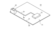
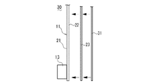
【解決手段】プリント回路基板11をシャーシ9の一部に略平行に隣接させて搭載し、シャーシ9をGNDベタパターン層として機能させる。さらに、プリント回路基板11とシャーシ9との間に絶縁体23を介在させることにより、信号ラインD+と信号ラインD−の周辺の浮遊容量を適正な範囲内で安定させる。これにより、USB信号ラインD+、D−の差動インピーダンスを規格内に収める。
【選択図】図3
Description
9 シャーシ
11 プリント回路基板
13 USB端子
21 第1層
22 第2層
D+ USB信号ライン
D− USB信号ライン
Claims (4)
- USB2.0の規格に準拠するUSB端子が実装され、画像形成装置の金属板から成るシャーシに搭載されるプリント回路基板において、
少なくともUSB信号ラインが形成された第1層と、少なくとも電源ラインが形成された第2層の2層で構成され、
前記シャーシに略平行に隣接して搭載され、
前記シャーシとの間に絶縁体が介在されていることにより、前記第1層と前記シャーシとの間の浮遊容量が適正化され、
前記シャーシを基板の略全領域をカバーするGNDベタパターン層として機能させることにより、基板内にGNDベタパターン層を設けることなく、USB信号ラインの差動インピーダンスをUSB2.0の規格内に収めて、2層基板を用いながらUSB2.0の規格に対応できるようにしたことを特徴とするプリント回路基板。 - 電子部品が実装され、信号ラインが形成されているプリント回路基板において、
金属板又は金属フィルムが基板と平行に隣接して配置され、該金属板又は金属フィルムが基板の略全領域をカバーするGNDベタパターン層として機能していることを特徴とするプリント回路基板。 - 前記金属板又は金属フィルムと基板の間には、絶縁体が介在されていることを特徴とする請求項2に記載のプリント回路基板。
- 請求項1乃至3に記載のプリント回路基板を備えたことを特徴とする電子機器。
Priority Applications (2)
| Application Number | Priority Date | Filing Date | Title |
|---|---|---|---|
| JP2005002360A JP4720184B2 (ja) | 2005-01-07 | 2005-01-07 | プリント回路基板及びそれを備えた電子機器 |
| US11/324,240 US20060154526A1 (en) | 2005-01-07 | 2006-01-04 | Printed circuit board and electronic apparatus equipped with the same |
Applications Claiming Priority (1)
| Application Number | Priority Date | Filing Date | Title |
|---|---|---|---|
| JP2005002360A JP4720184B2 (ja) | 2005-01-07 | 2005-01-07 | プリント回路基板及びそれを備えた電子機器 |
Publications (2)
| Publication Number | Publication Date |
|---|---|
| JP2006190873A true JP2006190873A (ja) | 2006-07-20 |
| JP4720184B2 JP4720184B2 (ja) | 2011-07-13 |
Family
ID=36653856
Family Applications (1)
| Application Number | Title | Priority Date | Filing Date |
|---|---|---|---|
| JP2005002360A Expired - Fee Related JP4720184B2 (ja) | 2005-01-07 | 2005-01-07 | プリント回路基板及びそれを備えた電子機器 |
Country Status (2)
| Country | Link |
|---|---|
| US (1) | US20060154526A1 (ja) |
| JP (1) | JP4720184B2 (ja) |
Cited By (3)
| Publication number | Priority date | Publication date | Assignee | Title |
|---|---|---|---|---|
| CN110471521A (zh) * | 2018-05-11 | 2019-11-19 | 丰田自动车株式会社 | 电子单元 |
| JP2020504440A (ja) * | 2016-12-08 | 2020-02-06 | 華為技術有限公司Huawei Technologies Co.,Ltd. | Usbポート付きデバイス |
| JP2021027337A (ja) * | 2019-08-06 | 2021-02-22 | キヤノン株式会社 | プリント回路板、プリント配線板、及び電子機器 |
Families Citing this family (8)
| Publication number | Priority date | Publication date | Assignee | Title |
|---|---|---|---|---|
| US7427719B2 (en) * | 2006-03-21 | 2008-09-23 | Intel Corporation | Shifted segment layout for differential signal traces to mitigate bundle weave effect |
| CN101472385A (zh) * | 2007-12-26 | 2009-07-01 | 鸿富锦精密工业(深圳)有限公司 | 印刷电路板 |
| EP2199920B1 (en) * | 2008-12-22 | 2013-09-18 | Huawei Device Co., Ltd. | Method and apparatus for improving radio performance of wireless data terminal device |
| CN201323599Y (zh) * | 2008-12-22 | 2009-10-07 | 深圳华为通信技术有限公司 | 一种无线数据终端设备 |
| CN201789539U (zh) * | 2010-09-09 | 2011-04-06 | 中兴通讯股份有限公司 | 一种移动终端 |
| CN102646086A (zh) * | 2011-02-18 | 2012-08-22 | 鸿富锦精密工业(深圳)有限公司 | Usb接口组件及其线路板 |
| CN105636421B (zh) * | 2016-01-22 | 2020-04-17 | 青岛海尔洗衣机有限公司 | 家用电器及减少干扰电压的装置 |
| CN109743834B (zh) * | 2018-12-28 | 2020-07-28 | 苏州浪潮智能科技有限公司 | 一种优化usb链路阻抗的方法 |
Citations (2)
| Publication number | Priority date | Publication date | Assignee | Title |
|---|---|---|---|---|
| JPS51113145A (en) * | 1975-03-31 | 1976-10-06 | Hitachi Ltd | Pluggin type relay |
| JPH11205012A (ja) * | 1998-01-14 | 1999-07-30 | Mitsubishi Electric Corp | 高周波回路 |
Family Cites Families (5)
| Publication number | Priority date | Publication date | Assignee | Title |
|---|---|---|---|---|
| US5761051A (en) * | 1994-12-29 | 1998-06-02 | Compaq Computer Corporation | Multi-layer circuit board having a supply bus and discrete voltage supply planes |
| JP2638567B2 (ja) * | 1995-06-08 | 1997-08-06 | 日本電気株式会社 | 多層配線基板 |
| US6140575A (en) * | 1997-10-28 | 2000-10-31 | 3Com Corporation | Shielded electronic circuit assembly |
| JP2003078279A (ja) * | 2001-09-04 | 2003-03-14 | Konica Corp | プリント基板のシールド方法及びその方法を用いたプリント基板が装着された装置 |
| US6650549B1 (en) * | 2002-10-23 | 2003-11-18 | D-Link Corp. | Hub having a bluetooth system |
-
2005
- 2005-01-07 JP JP2005002360A patent/JP4720184B2/ja not_active Expired - Fee Related
-
2006
- 2006-01-04 US US11/324,240 patent/US20060154526A1/en not_active Abandoned
Patent Citations (2)
| Publication number | Priority date | Publication date | Assignee | Title |
|---|---|---|---|---|
| JPS51113145A (en) * | 1975-03-31 | 1976-10-06 | Hitachi Ltd | Pluggin type relay |
| JPH11205012A (ja) * | 1998-01-14 | 1999-07-30 | Mitsubishi Electric Corp | 高周波回路 |
Cited By (6)
| Publication number | Priority date | Publication date | Assignee | Title |
|---|---|---|---|---|
| JP2020504440A (ja) * | 2016-12-08 | 2020-02-06 | 華為技術有限公司Huawei Technologies Co.,Ltd. | Usbポート付きデバイス |
| US10997109B2 (en) | 2016-12-08 | 2021-05-04 | Huawei Technologies Co., Ltd. | Device with USB port |
| CN110471521A (zh) * | 2018-05-11 | 2019-11-19 | 丰田自动车株式会社 | 电子单元 |
| CN110471521B (zh) * | 2018-05-11 | 2023-01-03 | 丰田自动车株式会社 | 电子单元 |
| JP2021027337A (ja) * | 2019-08-06 | 2021-02-22 | キヤノン株式会社 | プリント回路板、プリント配線板、及び電子機器 |
| JP7497232B2 (ja) | 2019-08-06 | 2024-06-10 | キヤノン株式会社 | プリント回路板、プリント配線板、及び電子機器 |
Also Published As
| Publication number | Publication date |
|---|---|
| JP4720184B2 (ja) | 2011-07-13 |
| US20060154526A1 (en) | 2006-07-13 |
Similar Documents
| Publication | Publication Date | Title |
|---|---|---|
| US9674941B2 (en) | Printed circuit board for mobile platforms | |
| US7435912B1 (en) | Tailoring via impedance on a circuit board | |
| US8063480B2 (en) | Printed board and semiconductor integrated circuit | |
| US8013427B2 (en) | Wiring board and electrical signal transmission system | |
| US20020108779A1 (en) | Multi-layered printed wiring board | |
| JP4720184B2 (ja) | プリント回路基板及びそれを備えた電子機器 | |
| US8022313B2 (en) | Circuit board with electromagnetic bandgap adjacent or overlapping differential signals | |
| JP4967164B2 (ja) | 多層プリント配線板及びそれを用いた電子機器 | |
| US20160233174A1 (en) | Integrated circuit, electronic device and method for transmitting data in electronic device | |
| CN220173699U (zh) | 电路模块 | |
| JP4660738B2 (ja) | プリント配線板及び電子機器 | |
| JP2004304134A (ja) | 配線基板及びその製造方法 | |
| US6812409B2 (en) | Layer allocating apparatus for multi-layer circuit board | |
| TWI706518B (zh) | 佈線基板 | |
| JP2001284828A (ja) | プリント基板 | |
| EP2996446A1 (en) | High speed routing module | |
| US8283574B2 (en) | Printed circuit board with compound via | |
| JP6889090B2 (ja) | 配線基板 | |
| JP2017220505A (ja) | プリント基板 | |
| CN118973079B (zh) | 印刷电路板、处理器和存储器之间的走线方法以及电子设备 | |
| JP2021028934A (ja) | プリント基板 | |
| US20260032822A1 (en) | Electronic module | |
| CN101018473B (zh) | 镜像式屏蔽结构 | |
| JP7528266B2 (ja) | Pcb組立体 | |
| JP6969847B2 (ja) | 配線基板 |
Legal Events
| Date | Code | Title | Description |
|---|---|---|---|
| A621 | Written request for application examination |
Free format text: JAPANESE INTERMEDIATE CODE: A621 Effective date: 20071213 |
|
| A977 | Report on retrieval |
Free format text: JAPANESE INTERMEDIATE CODE: A971007 Effective date: 20100216 |
|
| A131 | Notification of reasons for refusal |
Free format text: JAPANESE INTERMEDIATE CODE: A131 Effective date: 20100309 |
|
| A521 | Request for written amendment filed |
Free format text: JAPANESE INTERMEDIATE CODE: A523 Effective date: 20100428 |
|
| A131 | Notification of reasons for refusal |
Free format text: JAPANESE INTERMEDIATE CODE: A131 Effective date: 20100824 |
|
| A521 | Request for written amendment filed |
Free format text: JAPANESE INTERMEDIATE CODE: A523 Effective date: 20101025 |
|
| A01 | Written decision to grant a patent or to grant a registration (utility model) |
Free format text: JAPANESE INTERMEDIATE CODE: A01 Effective date: 20110308 |
|
| A61 | First payment of annual fees (during grant procedure) |
Free format text: JAPANESE INTERMEDIATE CODE: A61 Effective date: 20110321 |
|
| FPAY | Renewal fee payment (event date is renewal date of database) |
Free format text: PAYMENT UNTIL: 20140415 Year of fee payment: 3 |
|
| R150 | Certificate of patent or registration of utility model |
Free format text: JAPANESE INTERMEDIATE CODE: R150 |
|
| LAPS | Cancellation because of no payment of annual fees |