JP2006196687A - 磁気メモリ - Google Patents
磁気メモリ Download PDFInfo
- Publication number
- JP2006196687A JP2006196687A JP2005006647A JP2005006647A JP2006196687A JP 2006196687 A JP2006196687 A JP 2006196687A JP 2005006647 A JP2005006647 A JP 2005006647A JP 2005006647 A JP2005006647 A JP 2005006647A JP 2006196687 A JP2006196687 A JP 2006196687A
- Authority
- JP
- Japan
- Prior art keywords
- magnetic layer
- layer
- magnetic
- magnetization direction
- current
- Prior art date
- Legal status (The legal status is an assumption and is not a legal conclusion. Google has not performed a legal analysis and makes no representation as to the accuracy of the status listed.)
- Pending
Links
Images



Classifications
-
- G—PHYSICS
- G11—INFORMATION STORAGE
- G11C—STATIC STORES
- G11C11/00—Digital stores characterised by the use of particular electric or magnetic storage elements; Storage elements therefor
- G11C11/02—Digital stores characterised by the use of particular electric or magnetic storage elements; Storage elements therefor using magnetic elements
- G11C11/16—Digital stores characterised by the use of particular electric or magnetic storage elements; Storage elements therefor using magnetic elements using elements in which the storage effect is based on magnetic spin effect
-
- H—ELECTRICITY
- H10—SEMICONDUCTOR DEVICES; ELECTRIC SOLID-STATE DEVICES NOT OTHERWISE PROVIDED FOR
- H10B—ELECTRONIC MEMORY DEVICES
- H10B61/00—Magnetic memory devices, e.g. magnetoresistive RAM [MRAM] devices
- H10B61/20—Magnetic memory devices, e.g. magnetoresistive RAM [MRAM] devices comprising components having three or more electrodes, e.g. transistors
- H10B61/22—Magnetic memory devices, e.g. magnetoresistive RAM [MRAM] devices comprising components having three or more electrodes, e.g. transistors of the field-effect transistor [FET] type
-
- H—ELECTRICITY
- H10—SEMICONDUCTOR DEVICES; ELECTRIC SOLID-STATE DEVICES NOT OTHERWISE PROVIDED FOR
- H10N—ELECTRIC SOLID-STATE DEVICES NOT OTHERWISE PROVIDED FOR
- H10N50/00—Galvanomagnetic devices
- H10N50/10—Magnetoresistive devices
Landscapes
- Engineering & Computer Science (AREA)
- Computer Hardware Design (AREA)
- Mram Or Spin Memory Techniques (AREA)
- Hall/Mr Elements (AREA)
- Semiconductor Memories (AREA)
Abstract
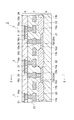
【解決手段】 磁気メモリ1が備えるTMR素子4は、積層方向に流れる電流の密度及びスピン方向に応じて磁化方向Aが変化する第1磁性層41と、第1磁性層41の一方の面41a上に設けられ、磁化方向Bが一定である第2磁性層43と、第1磁性層41と第2磁性層43との間に設けられた非磁性絶縁層42と、第1磁性層41の他方の面41b上に設けられ、磁化方向Cが一定である第3磁性層45と、第1磁性層41と第3磁性層45との間に設けられた第1非磁性導電層44とを備え、第1磁性層41における積層方向SLと直交する断面の面積が0.001μm2以上であり且つ0.02μm2を超えないことを特徴とする。
【選択図】 図4
Description
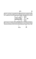
ここで、本実施形態による磁気メモリ1の変形例について説明する。図10〜図12は、それぞれ本変形例に係るTMR素子4a〜4cの構成を示す断面図である。上記実施形態のTMR素子4に代えて本変形例に係るTMR素子4a〜4cを磁気メモリが備えることによって、上記実施形態の磁気メモリ1と同様の効果を得ることができる。
Claims (7)
- 磁気抵抗効果素子を有する複数の記憶領域を備える磁気メモリであって、
前記磁気抵抗効果素子は、
強磁性材料を含み、積層方向に流れる電流の密度及びスピン方向に応じて磁化方向が変化する第1磁性層と、
強磁性材料を含み、前記第1磁性層の一方の面上に設けられ、磁化方向が一定である第2磁性層と、
非磁性材料を含み、前記第1磁性層と前記第2磁性層との間に設けられた非磁性層と、
強磁性材料を含み、前記第1磁性層の他方の面上に設けられ、磁化方向が一定である第3磁性層と、
非磁性且つ導電性の材料を含み、前記第1磁性層と前記第3磁性層との間に設けられた第1非磁性導電層と
を含み、
前記第1磁性層における前記積層方向と直交する断面の面積が0.001μm2以上であり且つ0.02μm2を超えないことを特徴とする、磁気メモリ。 - トンネル磁気抵抗効果素子を有する複数の記憶領域を備える磁気メモリであって、
前記トンネル磁気抵抗効果素子は、
強磁性材料を含み、積層方向に流れる電流の密度及びスピン方向に応じて磁化方向が変化する第1磁性層と、
強磁性材料を含み、前記第1磁性層の一方の面上に設けられ、磁化方向が一定である第2磁性層と、
非磁性且つ絶縁性の材料を含み、前記第1磁性層と前記第2磁性層との間に設けられた非磁性絶縁層と、
強磁性材料を含み、前記第1磁性層の他方の面上に設けられ、磁化方向が一定である第3磁性層と、
非磁性且つ導電性の材料を含み、前記第1磁性層と前記第3磁性層との間に設けられた第1非磁性導電層と
を含み、
前記第1磁性層における前記積層方向と直交する断面の面積が0.001μm2以上であり且つ0.02μm2を超えないことを特徴とする、磁気メモリ。 - 前記第2磁性層の前記積層方向の厚さが、前記第1磁性層の前記積層方向の厚さよりも大きいことを特徴とする、請求項1または2に記載の磁気メモリ。
- 前記第3磁性層の前記積層方向の厚さが、前記第1磁性層の前記積層方向の厚さよりも大きいことを特徴とする、請求項1〜3のいずれか一項に記載の磁気メモリ。
- 前記第2磁性層における前記積層方向と直交する断面の面積が、前記第1磁性層における前記積層方向と直交する断面の面積よりも大きいことを特徴とする、請求項1〜4のいずれか一項に記載の磁気メモリ。
- 反強磁性材料を含み、前記第2磁性層における前記第1磁性層と対向する面とは反対側の面上に設けられた反強磁性層を更に備えることを特徴とする、請求項1〜5のいずれか一項に記載の磁気メモリ。
- 強磁性材料を含み、前記第2磁性層における前記第1磁性層と対向する面とは反対側の面上に設けられた第4磁性層と、
非磁性且つ導電性の材料を含み、前記第2磁性層と前記第4磁性層との間に設けられた第2非磁性導電層と
を更に備えることを特徴とする、請求項1〜6のいずれか一項に記載の磁気メモリ。
Priority Applications (2)
| Application Number | Priority Date | Filing Date | Title |
|---|---|---|---|
| JP2005006647A JP2006196687A (ja) | 2005-01-13 | 2005-01-13 | 磁気メモリ |
| US11/330,196 US7366010B2 (en) | 2005-01-13 | 2006-01-12 | Magnetic memory |
Applications Claiming Priority (1)
| Application Number | Priority Date | Filing Date | Title |
|---|---|---|---|
| JP2005006647A JP2006196687A (ja) | 2005-01-13 | 2005-01-13 | 磁気メモリ |
Publications (1)
| Publication Number | Publication Date |
|---|---|
| JP2006196687A true JP2006196687A (ja) | 2006-07-27 |
Family
ID=36802521
Family Applications (1)
| Application Number | Title | Priority Date | Filing Date |
|---|---|---|---|
| JP2005006647A Pending JP2006196687A (ja) | 2005-01-13 | 2005-01-13 | 磁気メモリ |
Country Status (2)
| Country | Link |
|---|---|
| US (1) | US7366010B2 (ja) |
| JP (1) | JP2006196687A (ja) |
Families Citing this family (6)
| Publication number | Priority date | Publication date | Assignee | Title |
|---|---|---|---|---|
| JP4758812B2 (ja) * | 2006-04-26 | 2011-08-31 | 株式会社日立製作所 | スピン流狭窄層を備えたスピン蓄積素子及びその作製方法 |
| US7539046B2 (en) * | 2007-01-31 | 2009-05-26 | Northern Lights Semiconductor Corp. | Integrated circuit with magnetic memory |
| JP4682998B2 (ja) * | 2007-03-15 | 2011-05-11 | ソニー株式会社 | 記憶素子及びメモリ |
| JP2010114143A (ja) * | 2008-11-04 | 2010-05-20 | Toshiba Corp | 半導体記憶装置および半導体記憶装置の製造方法 |
| US9583187B2 (en) * | 2015-03-28 | 2017-02-28 | Intel Corporation | Multistage set procedure for phase change memory |
| CN108666339B (zh) * | 2017-03-28 | 2020-11-13 | 中芯国际集成电路制造(上海)有限公司 | 磁性随机存储器及其存储单元的制造方法 |
Citations (5)
| Publication number | Priority date | Publication date | Assignee | Title |
|---|---|---|---|---|
| JP2001156357A (ja) * | 1999-09-16 | 2001-06-08 | Toshiba Corp | 磁気抵抗効果素子および磁気記録素子 |
| WO2003025942A2 (fr) * | 2001-09-20 | 2003-03-27 | Centre National De La Recherche Scientifique | Memoire magnetique a ecriture par courant polarise en spin, mettant en oeuvre des alliages amorphes ferrimagnetiques et procede pour son ecriture |
| WO2004013861A2 (en) * | 2002-08-06 | 2004-02-12 | Grandis, Inc. | Magnetic element utilizing spin transfer and an mram device using the magnetic element |
| JP2004207707A (ja) * | 2002-12-13 | 2004-07-22 | Japan Science & Technology Agency | スピン注入デバイス及びこれを用いた磁気装置 |
| JP2005150482A (ja) * | 2003-11-18 | 2005-06-09 | Sony Corp | 磁気抵抗効果素子及び磁気メモリ装置 |
Family Cites Families (18)
| Publication number | Priority date | Publication date | Assignee | Title |
|---|---|---|---|---|
| JP3022023B2 (ja) * | 1992-04-13 | 2000-03-15 | 株式会社日立製作所 | 磁気記録再生装置 |
| JPH0766033A (ja) * | 1993-08-30 | 1995-03-10 | Mitsubishi Electric Corp | 磁気抵抗素子ならびにその磁気抵抗素子を用いた磁性薄膜メモリおよび磁気抵抗センサ |
| JPH08274386A (ja) * | 1995-03-31 | 1996-10-18 | Mitsubishi Electric Corp | 磁電変換素子 |
| US5768181A (en) * | 1997-04-07 | 1998-06-16 | Motorola, Inc. | Magnetic device having multi-layer with insulating and conductive layers |
| JP4066477B2 (ja) | 1997-10-09 | 2008-03-26 | ソニー株式会社 | 不揮発性ランダムアクセスメモリー装置 |
| EP1115164B1 (en) * | 2000-01-07 | 2005-05-25 | Sharp Kabushiki Kaisha | Magnetoresistive device and magnetic memory using the same |
| US6469926B1 (en) * | 2000-03-22 | 2002-10-22 | Motorola, Inc. | Magnetic element with an improved magnetoresistance ratio and fabricating method thereof |
| JP4020573B2 (ja) * | 2000-07-27 | 2007-12-12 | 富士通株式会社 | 磁性メモリデバイス、および磁性メモリデバイスにおけるデータ読み出し方法 |
| US6347049B1 (en) * | 2001-07-25 | 2002-02-12 | International Business Machines Corporation | Low resistance magnetic tunnel junction device with bilayer or multilayer tunnel barrier |
| JP3967237B2 (ja) | 2001-09-19 | 2007-08-29 | 株式会社東芝 | 磁気抵抗効果素子及びその製造方法、磁気再生素子並びに磁気メモリ |
| JP3980990B2 (ja) | 2002-10-31 | 2007-09-26 | 株式会社東芝 | 磁気メモリ |
| US7023723B2 (en) * | 2002-11-12 | 2006-04-04 | Nve Corporation | Magnetic memory layers thermal pulse transitions |
| CN101114694A (zh) * | 2002-11-26 | 2008-01-30 | 株式会社东芝 | 磁单元和磁存储器 |
| JP2004179483A (ja) * | 2002-11-28 | 2004-06-24 | Hitachi Ltd | 不揮発性磁気メモリ |
| JP4147118B2 (ja) * | 2003-01-15 | 2008-09-10 | 株式会社日立製作所 | 3端子型磁気ヘッドとそれを搭載した磁気記録再生装置 |
| US6667901B1 (en) * | 2003-04-29 | 2003-12-23 | Hewlett-Packard Development Company, L.P. | Dual-junction magnetic memory device and read method |
| JP2006032464A (ja) * | 2004-07-13 | 2006-02-02 | Toshiba Corp | 磁気ランダムアクセスメモリ |
| JP2006196683A (ja) * | 2005-01-13 | 2006-07-27 | Tdk Corp | 磁気抵抗効果素子及び磁気メモリ |
-
2005
- 2005-01-13 JP JP2005006647A patent/JP2006196687A/ja active Pending
-
2006
- 2006-01-12 US US11/330,196 patent/US7366010B2/en not_active Expired - Lifetime
Patent Citations (5)
| Publication number | Priority date | Publication date | Assignee | Title |
|---|---|---|---|---|
| JP2001156357A (ja) * | 1999-09-16 | 2001-06-08 | Toshiba Corp | 磁気抵抗効果素子および磁気記録素子 |
| WO2003025942A2 (fr) * | 2001-09-20 | 2003-03-27 | Centre National De La Recherche Scientifique | Memoire magnetique a ecriture par courant polarise en spin, mettant en oeuvre des alliages amorphes ferrimagnetiques et procede pour son ecriture |
| WO2004013861A2 (en) * | 2002-08-06 | 2004-02-12 | Grandis, Inc. | Magnetic element utilizing spin transfer and an mram device using the magnetic element |
| JP2004207707A (ja) * | 2002-12-13 | 2004-07-22 | Japan Science & Technology Agency | スピン注入デバイス及びこれを用いた磁気装置 |
| JP2005150482A (ja) * | 2003-11-18 | 2005-06-09 | Sony Corp | 磁気抵抗効果素子及び磁気メモリ装置 |
Also Published As
| Publication number | Publication date |
|---|---|
| US7366010B2 (en) | 2008-04-29 |
| US20060186443A1 (en) | 2006-08-24 |
Similar Documents
| Publication | Publication Date | Title |
|---|---|---|
| JP6200471B2 (ja) | 磁気メモリ | |
| US7012832B1 (en) | Magnetic memory cell with plural read transistors | |
| US8779496B2 (en) | Spin FET, magnetoresistive element and spin memory | |
| JP4693634B2 (ja) | スピンfet | |
| US7535755B2 (en) | Magnetic memory device and method for fabricating the same | |
| US10483459B2 (en) | Magnetic memory | |
| US20100109061A1 (en) | Semiconductor memory device and manufacturing method for semiconductor memory device | |
| US10170694B1 (en) | Magnetic memory | |
| US11730001B2 (en) | Tunnel magnetoresistive effect element, magnetic memory, and built-in memory | |
| CN102280136A (zh) | 磁存储器元件和磁存储器器件 | |
| JP2008187048A (ja) | 磁気抵抗効果素子 | |
| JP2007317895A (ja) | 磁気抵抗メモリ装置 | |
| JP4729836B2 (ja) | 磁気記憶セルおよび磁気メモリデバイスならびに磁気メモリデバイスの製造方法 | |
| US7366010B2 (en) | Magnetic memory | |
| US7522450B2 (en) | Magnetic storage cell, magnetic memory device and magnetic memory device manufacturing method | |
| JP2006278645A (ja) | 磁気メモリ装置 | |
| US20070133264A1 (en) | Storage element and memory | |
| US7683446B2 (en) | Magnetic memory using spin injection flux reversal | |
| JP2006196683A (ja) | 磁気抵抗効果素子及び磁気メモリ | |
| KR20070066118A (ko) | 자기터널접합 셀 및 이를 구비하는 자기램 | |
| JP2006156893A (ja) | 磁気メモリ | |
| JP2009146995A (ja) | 磁気記憶装置 | |
| JP2007123512A (ja) | 磁気記憶装置 | |
| EP1635356A1 (en) | Magnetic memory with magnetic yoke |
Legal Events
| Date | Code | Title | Description |
|---|---|---|---|
| A621 | Written request for application examination |
Free format text: JAPANESE INTERMEDIATE CODE: A621 Effective date: 20070911 |
|
| A977 | Report on retrieval |
Free format text: JAPANESE INTERMEDIATE CODE: A971007 Effective date: 20100723 |
|
| A131 | Notification of reasons for refusal |
Free format text: JAPANESE INTERMEDIATE CODE: A131 Effective date: 20100727 |
|
| A521 | Request for written amendment filed |
Free format text: JAPANESE INTERMEDIATE CODE: A523 Effective date: 20100921 |
|
| A02 | Decision of refusal |
Free format text: JAPANESE INTERMEDIATE CODE: A02 Effective date: 20110322 |