JP2006198738A - Punching die for printed circuit board - Google Patents
Punching die for printed circuit board Download PDFInfo
- Publication number
- JP2006198738A JP2006198738A JP2005014056A JP2005014056A JP2006198738A JP 2006198738 A JP2006198738 A JP 2006198738A JP 2005014056 A JP2005014056 A JP 2005014056A JP 2005014056 A JP2005014056 A JP 2005014056A JP 2006198738 A JP2006198738 A JP 2006198738A
- Authority
- JP
- Japan
- Prior art keywords
- printed circuit
- circuit board
- die plate
- punching
- lower die
- Prior art date
- Legal status (The legal status is an assumption and is not a legal conclusion. Google has not performed a legal analysis and makes no representation as to the accuracy of the status listed.)
- Pending
Links
- 238000004080 punching Methods 0.000 title claims abstract description 76
- 239000000463 material Substances 0.000 claims abstract description 58
- 230000002093 peripheral effect Effects 0.000 claims abstract description 9
- 239000002994 raw material Substances 0.000 claims description 2
- 238000003825 pressing Methods 0.000 abstract description 4
- 230000000740 bleeding effect Effects 0.000 abstract 1
- 239000000758 substrate Substances 0.000 description 12
- 238000000034 method Methods 0.000 description 10
- 125000006850 spacer group Chemical group 0.000 description 4
- 238000003780 insertion Methods 0.000 description 2
- 230000037431 insertion Effects 0.000 description 2
- 239000002184 metal Substances 0.000 description 2
- 229920006311 Urethane elastomer Polymers 0.000 description 1
- 230000006835 compression Effects 0.000 description 1
- 238000007906 compression Methods 0.000 description 1
- 238000009434 installation Methods 0.000 description 1
- 238000007747 plating Methods 0.000 description 1
Images





Landscapes
- Perforating, Stamping-Out Or Severing By Means Other Than Cutting (AREA)
Abstract
Description
本発明は、プリント基板打抜き用金型に関する。 The present invention relates to a printed board punching die.
従来、プリント基板の外形抜きやスリット抜きを行う場合、打抜きプレス加工機などに取り付けられたプリント基板打抜き用金型を用いてプリント基板素材を打抜くことにより行われていた。このようなプリント基板打抜き用金型として、例えば特許文献1に開示されたものがある。 Conventionally, when performing external cutting or slitting of a printed circuit board, it has been performed by punching a printed circuit board material using a printed circuit board punching die attached to a punching press or the like. An example of such a printed circuit board punching die is disclosed in Patent Document 1.
特許文献1に開示されているようなプリント基板打抜き用金型の基本構成は、図12に示すように、プリント基板素材150からプリント基板を打抜くための上型110と下型120とを備えている。上型110は、図示しない打抜きプレス加工機に取り付けるための天板プレート111、上型の厚さを調節するためのスペーサーダイホルダー112およびプリント基板の外形を切断するための上型ダイプレート113を備えている。
As shown in FIG. 12, the basic configuration of a printed board punching die disclosed in Patent Document 1 includes an
上型ダイプレート113は、断面矩形状の金属部材により形成されている。上型ダイプレート113の下型ダイプレート121に対向する面には、下型ダイプレート121が嵌入する凹部(シェダー)114が形成されている。また、シェダー114の開口縁115は、プリント基板素材150を切断する機能を有している。
The
シェダー114の周囲の面は、下型ダイプレート121およびストリッパー122に載置されるプリント基板素材150と平行となるように形成された支持面116であり、後述するストリッパー122との間でプリント基板150を挟持する機能を有している。
The peripheral surface of the
下型120は、下型ダイプレート121、ストリッパー122、弾性部材123およびアンダーダイプレート124を備えている。下型ダイプレート121は、シェダー114の開口縁115により切断されたプリント基板をプリント基板素材150から抜くための部材である。この下型ダイプレート121は、上型ダイプレート113のシェダー114の内周面と同一形状となるように形成されており、上型110の降下に伴ってシェダー114の内周面に沿って嵌入するように構成されている。また、下型ダイプレート121の上面は水平面となるように形成されている。
The lower die 120 includes a
ストリッパー122は、プリント基板を打抜く際に、上型ダイプレート113の支持面116との間でプリント基板素材150を挟持するための部材である。このストリッパー122には、下型ダイプレート121と同一形状の貫通孔が設けられており、下型ダイプレート121の側壁面125に沿って弾性的に上下動可能となるように、弾性部材123を介してアンダーダイプレート124に取り付けられている。また、上型110と下型120とを開いた状態において、ストリッパー122は、その上面と下型ダイプレート121の上面とが略面一となるように構成されている。弾性部材123の材質は特に限定されるものではないが、ウレタンゴムを好適な一例として挙げることができる。
The
アンダーダイプレート124は、下型120の土台を構成する部材であり、上面に下型ダイプレート121および弾性部材123が取り付けられている。
The under
このように構成されたプリント基板打抜き用金型100を用いてプリント基板の打抜き加工を行うには、プリント基板打抜き用金型100を打抜きプレス加工機などに取り付け、プリント基板素材150を下型ダイプレート121上の所定位置に載せた後、上型110を降下させて、上型ダイプレート113と下型ダイプレート121とを嵌合させることにより行う。
しかしながら、上述したプリント基板打抜き用金型を用いてプリント基板の打抜き加工を行う場合、シェダーの開口縁による切断時の衝撃により切断位置にズレが生じていた。また、プリント基板素材の切断時に、図13に示すように、シェダー114の開口縁115に囲まれているプリント基板素材150が隆起することにより切断位置にズレが生じていた。
However, when a printed circuit board is punched using the above-described printed circuit board punching die, the cutting position is displaced due to an impact at the time of cutting by the opening edge of the shedder. Further, when the printed circuit board material was cut, as shown in FIG. 13, the printed
このように従来において用いられているプリント基板打抜き用金型によってプリント基板の打抜き加工を行った場合、プリント基板の切断位置にズレが発生することから、プリント基板の切断面にヒゲ、バリなどが発生すると共に、高い寸法精度で打抜き加工を行うことが困難であるという問題があった。 As described above, when the printed circuit board is punched by the conventionally used printed circuit board punching die, the cutting position of the printed circuit board is displaced, so that the cut surface of the printed circuit board has beards, burrs, and the like. There is a problem that it is difficult to perform punching with high dimensional accuracy.
本発明は、このような問題を解決すべくなされたものであって、プリント基板の切断面にヒゲ、バリなどが発生することを防止しつつ、高い寸法精度で打抜き加工ができるプリント基板打抜き用金型の提供を目的とする。 The present invention has been made to solve such a problem, and is for punching a printed circuit board that can be punched with high dimensional accuracy while preventing the occurrence of whiskers, burrs, etc. on the cut surface of the printed circuit board. The purpose is to provide molds.
本発明の上記目的は、プリント基板素材が載置される下型ダイプレートと、凹部が形成された上型ダイプレートとを備えており、前記下型ダイプレートに載置されたプリント基板素材を前記上型ダイプレートで押圧することにより、前記下型ダイプレートが前記凹部に嵌入してプリント基板素材からプリント基板を打抜くことが可能なプリント基板打抜き用金型において、前記凹部の開口縁は、前記下型ダイプレートに載置されたプリント基板素材の表面に対して傾斜しており、前記上型ダイプレートにおける前記凹部の周囲には、前記上型ダイプレートの押圧時に前記下型ダイプレートに載置されたプリント基板素材の周縁部が反り上がることを可能とする逃げ部が設けられているプリント基板打抜き用金型により達成される。 The object of the present invention includes a lower die plate on which a printed board material is placed, and an upper die plate in which a recess is formed, and the printed board material placed on the lower die plate is In the printed circuit board punching die in which the lower mold plate can be inserted into the concave portion and punched out of the printed circuit board material by pressing with the upper die plate, the opening edge of the concave portion is The lower die plate is inclined with respect to the surface of the printed circuit board material placed on the lower die plate, and around the concave portion of the upper die plate when the upper die plate is pressed. This is achieved by a printed circuit board punching die provided with a relief portion that allows the peripheral edge portion of the printed circuit board material placed on the substrate to warp.
このプリント基板打抜き用金型において、前記逃げ部は、縦断面視において直線状に傾斜する傾斜面であることが好ましい。 In this printed board punching die, the escape portion is preferably an inclined surface that is linearly inclined in a longitudinal sectional view.
また、前記凹部は、多角形状に形成されており、各角部に前記下型ダイプレートに載置されたプリント基板素材に対して平行となる支持面が形成されていることが好ましい。 Moreover, it is preferable that the said recessed part is formed in polygonal shape, and the support surface which becomes parallel with respect to the printed circuit board raw material mounted in the said lower die | dye plate is formed in each corner | angular part.
また、前記凹部の開口縁は、前記下型ダイプレートの嵌入方向に窪むV字状に形成されていることが好ましい。 Moreover, it is preferable that the opening edge of the said recessed part is formed in the V shape recessed in the insertion direction of the said lower die plate.
本発明によれば、プリント基板の切断面にヒゲ、バリなどが発生することを防止しつつ、高い寸法精度で打抜き加工ができるプリント基板打抜き用金型を提供することができる。 According to the present invention, it is possible to provide a printed circuit board punching die that can perform punching with high dimensional accuracy while preventing generation of whiskers, burrs, and the like on the cut surface of the printed circuit board.
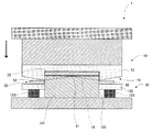
以下、本発明のプリント基板打抜き用金型について添付図面を参照して説明する。図1は本発明の一実施形態に係るプリント基板打抜き用金型1の断面図であり、図示しない打抜きプレス加工機に取り付けた状態を示している。図1に示すように、プリント基板打抜き用金型1は、互いに嵌合することによりプリント基板素材50からプリント基板を打抜くための上型10と下型30とを備えている。なお、下型30の構成は、背景技術で説明した図12に示される下型120と同じであるため、下型120の構成部材と同一の部材については、同一の符号を付すると共に、詳細な説明は省略する。
Hereinafter, a printed board punching die according to the present invention will be described with reference to the accompanying drawings. FIG. 1 is a cross-sectional view of a printed circuit board punching die 1 according to an embodiment of the present invention, showing a state where the printed board punching die 1 is attached to a punching press machine (not shown). As shown in FIG. 1, the printed circuit board punching die 1 includes an
上型10は、打抜きプレス加工機に取り付けるための天板プレート11、上型の厚さを調節するためのスペーサーダイホルダー12およびプリント基板の外形を切断するための上型ダイプレート13を備えている。スペーサーダイホルダー12は、ボルトなどを介して天板プレート11に固定されており、上型ダイプレート13は、ボルトなどを介してスペーサーダイホルダー12に固定されている。
The
上型ダイプレート13の下型ダイプレート121の上面に対向する面には、下型ダイプレート121が嵌入する凹部(以下、シェダーという)14が形成されている。シェダー14の平面視形状は図2に示すように矩形状に形成されており、この平面視形状がプリント基板の打抜き形状となる。また、シェダー14の平面視形状は、矩形状に限定されるものではなく、例えば、三角形状、五角形状などの多角形状とすることができる。また、円形状とすることもできる。
On the surface facing the upper surface of the
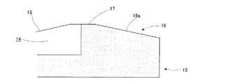
シェダー14の開口縁15は、プリント基板素材50を切断する機能を有している。この開口縁15は、下型ダイプレート121に載置されたプリント基板素材50の表面に対して傾斜しており、下型ダイプレート121の嵌入方向に窪むV字状に形成されている。
The
また、上型ダイプレートにおけるシェダー14の周囲には、後述するように、下型ダイプレート121に載置されたプリント基板素材50を上型ダイプレート13が押圧するときに、プリント基板素材50の周縁部が反り上がることを可能とする逃げ部16が設けられている。この逃げ部16は、縦断面視において、直線状に傾斜する傾斜面16aとなるように形成されている。
As will be described later, when the
このように構成されたプリント基板打抜き用金型1を用いて、プリント基板の打抜き加工を行う方法について図1及び図3から図5を用いて、以下に説明する。まず、図1に示すように、図示しない打抜きプレス加工機に固定されたプリント基板打抜き用金型1の上型10と下型30とを開き、プリント基板素材50を下型30の下型ダイプレート121に載せる。
A method for punching a printed circuit board using the printed circuit board punching die 1 configured as described above will be described below with reference to FIGS. 1 and 3 to 5. First, as shown in FIG. 1, the
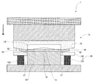
次に、打抜きプレス加工機を作動させ、上型10を降下させると、図3に示すように、シェダー14の各角部15aがプリント基板素材50に当接する。このとき、上型ダイプレート13の押圧により、プリント基板素材50の周縁部(以下、捨て基板52という)が反り上がるが、シェダー14の開口縁15で囲まれているプリント基板素材(以下、プリント基板51という)には隆起が発生しない。
Next, when the punching press machine is operated and the
更に、上型10を降下させて、下型ダイプレート121に載置されたプリント基板素材50を上型ダイプレート13で押圧すると、図4に示すように、シェダー14の開口縁15がプリント基板素材50に侵入して切断が行われる。このとき、下型ダイプレート121は、上型ダイプレート13の降下10に伴いシェダー14内に嵌入していく。また、ストリッパー122は、シェダー14の各角部15aにより捨て基板52を介して押圧され、弾性部材123の圧縮変形に伴い、下型ダイプレート121の側壁面125に沿って下方に移動していく。
Further, when the
プリント基板素材50の切断は、シェダー14の開口縁15がV字状に傾斜しているため、開口縁15とプリント基板素材50とが当接している一部分で行われる。したがって、開口縁15とプリント基板素材50との当接部分に打抜き力が集中するため、容易にかつ確実に切断することが可能となる。また、開口縁15が傾斜しているため、上型10の降下に伴い、プリント基板素材50を徐々に切断することができ、打抜き時の衝撃力を緩和させることができる。この結果、打抜き加工時にプリント基板素材50の位置ズレが発生することや、上型ダイプレート13と下型ダイプレート121との間に位置ズレが発生することを防止することができる。
The cutting of the printed
また、上型10の降下により、捨て基板52の外側は、図3に示す状態よりも更に反り上がり、捨て基板52は、逃げ部16の傾斜面16aに沿って当接する。このように、上型ダイプレートの押圧時に、捨て基板52が反り上がることが可能な逃げ部16をシェダー14の周囲に設けたことにより、打抜き加工時に発生するプリント基板素材50の変形を、捨て基板52側に発生させ、プリント基板51側に発生することを防止することができる。この結果、打抜かれるプリント基板51の姿勢を、下型ダイプレート121の上面と平行となるように維持して打抜き加工を行うことができるので、プリント基板51の切断位置にズレが発生することや、切断面にヒゲ、バリなどが発生することを防止することができる。また、切断位置にズレが発生することを防止して、安定して打抜き加工を行うことができるため、打抜き加工時に発生する衝撃力を低下させることができる。
Further, due to the lowering of the
また、逃げ部16は、縦断面視において、直線状に傾斜する傾斜面16aとなるように形成されているため、打抜き加工時に反り上がった捨て基板52を当該傾斜面16aに沿って安定して押えることができる。したがって、プリント基板素材50が、図4の左右方向に移動することを防止することができ、プリント基板51の切断位置にズレが発生することを効果的に防止することができる。
Further, since the
更に上型ダイプレート13の降下が進んで、図5に示すようにシェダー14の開口縁15の全域がプリント基板素材50を貫通することにより、プリント基板素材50からプリント基板51が切り離される。その後、上型10を上昇させてプリント基板51を取り除くことにより打抜き加工は完了する。なお、プリント基板51がプリント基板素材50から切り離されると、捨て基板52は、ストリッパー122の上面と平行な姿勢となり、ストリッパー122上に残る。また、上型10の上昇に伴い、ストリッパー122は、弾性部材123の弾性復元力により、その上面が下型ダイプレート121の上面と略面一となる位置まで下型ダイプレート121の側壁面125に沿って上昇する。
Further, the
ここで、図1に示すV字状の開口縁15の傾斜深さwは、プリント基板素材50の板厚に対して、110%から200%の範囲が好ましく、特に、120%から150%の範囲がより好ましい。本実施形態においては、開口縁15の傾斜深さwを、プリント基板素材50の板厚寸法に対して120%の寸法としている。この数値範囲外でも使用することはできるが、開口縁15の傾斜深さwが小さすぎると、プリント基板素材50に打抜き加工を施した場合に、切断時の衝撃などにより、切断位置にズレが生じ、プリント基板51の切断面にヒゲ、バリが発生するおそれがある。一方、開口縁15の傾斜深さwが大きすぎると、開口縁15による切断が完了する前にプリント基板51が割れて打抜かれるおそれがある。
Here, the inclination depth w of the V-shaped
また、逃げ部16の傾斜面16aの傾斜角θは、水平線に対して5°から20°の範囲が好ましく、特に、5°から10°の範囲がより好ましい。本実施形態においては、傾斜角θを10°としている。この数値範囲外でも使用することはできるが、傾斜角θが小さすぎると、打抜き加工時において、プリント基板51側に隆起が発生するおそれがあり、プリント基板51の切断面にヒゲ、バリが発生するおそれがある。一方、傾斜角θが大きすぎると、反り上がった捨て基板52を逃げ部16の傾斜面16aにて押えることが困難となり、プリント基板素材50の設置位置が変化して切断位置にズレが生じるおそれがある。
Further, the inclination angle θ of the
このように本実施形態に係るプリント基板打抜き用金型1によれば、打抜き加工時に発生する衝撃力を低下させることができ、また、シェダー14の開口縁15で囲まれているプリント基板51が隆起することを防止しつつ、確実に切断することができるため、切断位置にズレが発生することを防止することができる。その結果、プリント基板51の切断面にヒゲ、バリが発生することを防止できると共に、高い寸法精度でプリント基板51の打抜き加工を行うことができる。
As described above, according to the printed circuit board punching die 1 according to the present embodiment, the impact force generated during the punching process can be reduced, and the printed
また、打抜き加工時に発生する衝撃力を小さくすることができるので、打抜き時の衝撃によって上型ダイプレート13と下型ダイプレート121との間に位置ズレが発生することを防止することができる。したがって、上型ダイプレート13のシェダー14の内周面と下型ダイプレート121の外壁面125とのクリアランスを極めて小さく設定することができ、高い寸法精度でプリント基板の打抜き加工を行うことができる。
Further, since the impact force generated during the punching process can be reduced, it is possible to prevent the positional deviation between the
また、本実施形態に係るプリント基板打抜き用金型を用いて、スルーホールが形成されたプリント基板に打抜き加工を行い、スルーホールハーフカット基板を形成する場合においても、ハーフカットが施されるスルーホールの切断位置が、打抜き加工時に変動しないため、スルーホールの内壁メッキ部に剥離やひび割れなどが発生することを防止することができる。 In addition, when a through-hole half-cut substrate is formed by punching a printed circuit board having a through-hole formed therein using the printed-circuit board punching die according to the present embodiment, a through-cut is performed. Since the hole cutting position does not change during punching, it is possible to prevent the inner wall plating portion of the through hole from being peeled off or cracked.
また、ハロゲンフリー材により形成したプリント基板の打抜き加工を行う場合においても、シェダー14の開口縁15により囲まれているプリント基板51の隆起を防止しつつ、大きな力で確実に切断することができるため、切断面が破壊されて虫食い状態となることを防止することができると共に、高い寸法精度で打抜き加工を行うことができる。
Even when a printed board formed of a halogen-free material is punched, the printed
以上、本発明の一実施形態について説明したが、本発明の具体的な態様は上記実施形態に限定されない。例えば、図6の平面図および図6のA−A断面の要部拡大図である図7に示すように、下型ダイプレート121に載置されたプリント基板素材50に対して平行となる支持面17をシェダー14の各角部15aに設けてもよい。このような構成のプリント基板打抜き用金型1によりプリント基板の打抜き加工を行った場合、図8に示すように、支持面17とストリッパー122の上面とによりプリント基板素材50の捨て基板52側を確実に挟持することができる。したがって、打抜き加工時において、プリント基板素材50の位置ズレが発生することを確実に防止することができるため、切断面にヒゲ、バリなどが発生することを確実に防止できると共に、高い寸法精度でプリント基板の打抜き加工を行うことができる。
As mentioned above, although one Embodiment of this invention was described, the specific aspect of this invention is not limited to the said embodiment. For example, as shown in FIG. 7, which is a plan view of FIG. 6 and an enlarged view of the main part of the AA cross section of FIG. 6, a support that is parallel to the printed
また、本実施形態においては、逃げ部16は、縦断面視において、直線状に傾斜する傾斜面16aとなるように形成されているが、例えば、図9に示すように、湾曲状に傾斜する傾斜面16aとなるように形成してもよい。なお、この湾曲状の傾斜面16aは、縦断面視において、上に突あるいは下に突のいずれであってもよい。
Further, in the present embodiment, the
また、本実施形態において、シェダー14の開口縁15は、V字状に形成されているが、例えば、図10に示すように、曲線状に形成してもよい。このような構成であっても、プリント基板素材50の切断は、開口縁15とプリント基板素材50とが当接している一部分で行われるので、この当接部分に打抜き力が集中し、容易にかつ確実にプリント基板素材50を切断することが可能となる。また、上型10の降下に伴い、プリント基板素材50を徐々に切断することができ、打抜き時の衝撃力を緩和させることができるので、上型ダイプレート13と下型ダイプレート121との位置ズレを防止することができる。
In the present embodiment, the opening
また、シェダー14の開口縁15の形状をV字状とする代わりに、図11に示すように、片側に傾斜する直線形状としてもよい。
Moreover, instead of making the shape of the opening
1 プリント基板打抜き用金型
10 上型
13 上型ダイプレート
14 凹部(シェダー)
15 開口縁
15a 角部
16 逃げ部
16a 傾斜面
17 支持面
30 下型
50 プリント基板素材
51 プリント基板
52 捨て基板
121 下型ダイプレート
122 ストリッパー
DESCRIPTION OF SYMBOLS 1 Die for printed
15
Claims (4)
前記凹部の開口縁は、前記下型ダイプレートに載置されたプリント基板素材の表面に対して傾斜しており、
前記上型ダイプレートにおける前記凹部の周囲には、前記上型ダイプレートの押圧時に前記下型ダイプレートに載置されたプリント基板素材の周縁部が反り上がることを可能とする逃げ部が設けられているプリント基板打抜き用金型。 A lower die plate on which a printed board material is placed and an upper die plate with a recess formed thereon, and the printed board material placed on the lower die plate is pressed by the upper die plate In the printed circuit board punching die capable of punching the printed circuit board from the printed circuit board material by fitting the lower die plate into the recess,
The opening edge of the recess is inclined with respect to the surface of the printed circuit board material placed on the lower die plate,
Around the concave portion of the upper die plate, there is provided an escape portion that allows the peripheral portion of the printed circuit board material placed on the lower die plate to warp when the upper die plate is pressed. Die for punching printed circuit boards.
4. The printed circuit board punching die according to claim 1, wherein an opening edge of the concave portion is formed in a V shape that is recessed in a fitting direction of the lower die plate. 5.
Priority Applications (1)
| Application Number | Priority Date | Filing Date | Title |
|---|---|---|---|
| JP2005014056A JP2006198738A (en) | 2005-01-21 | 2005-01-21 | Punching die for printed circuit board |
Applications Claiming Priority (1)
| Application Number | Priority Date | Filing Date | Title |
|---|---|---|---|
| JP2005014056A JP2006198738A (en) | 2005-01-21 | 2005-01-21 | Punching die for printed circuit board |
Publications (1)
| Publication Number | Publication Date |
|---|---|
| JP2006198738A true JP2006198738A (en) | 2006-08-03 |
Family
ID=36957166
Family Applications (1)
| Application Number | Title | Priority Date | Filing Date |
|---|---|---|---|
| JP2005014056A Pending JP2006198738A (en) | 2005-01-21 | 2005-01-21 | Punching die for printed circuit board |
Country Status (1)
| Country | Link |
|---|---|
| JP (1) | JP2006198738A (en) |
Cited By (6)
| Publication number | Priority date | Publication date | Assignee | Title |
|---|---|---|---|---|
| WO2012127672A1 (en) * | 2011-03-24 | 2012-09-27 | 株式会社メイコー | Method and apparatus for cutting substrate |
| CN103722589A (en) * | 2012-10-12 | 2014-04-16 | 珠海格力电器股份有限公司 | Shutter mould |
| CN104290136A (en) * | 2014-09-12 | 2015-01-21 | 东莞市合通电子有限公司 | Unilateral rim charge removing device of PCB and rim charge removing method of unilateral rim charge removing device |
| CN105196353A (en) * | 2014-06-24 | 2015-12-30 | 嘉联益科技股份有限公司 | punching tool |
| CN114882041A (en) * | 2022-07-12 | 2022-08-09 | 江苏紫琅汽车集团股份有限公司 | Voting and identification method for burrs inside cast iron pipeline |
| CN115884520A (en) * | 2022-11-25 | 2023-03-31 | 武平飞天电子科技有限公司 | A 5G base station antenna coupling printed circuit board manufacturing method |
-
2005
- 2005-01-21 JP JP2005014056A patent/JP2006198738A/en active Pending
Cited By (11)
| Publication number | Priority date | Publication date | Assignee | Title |
|---|---|---|---|---|
| WO2012127672A1 (en) * | 2011-03-24 | 2012-09-27 | 株式会社メイコー | Method and apparatus for cutting substrate |
| CN103442860A (en) * | 2011-03-24 | 2013-12-11 | 名幸电子有限公司 | Method and apparatus for cutting substrate |
| JP5499218B2 (en) * | 2011-03-24 | 2014-05-21 | 株式会社メイコー | Substrate shearing method and apparatus |
| TWI492685B (en) * | 2011-03-24 | 2015-07-11 | Meiko Electronics Co Ltd | Substrate cutting method and device |
| CN103442860B (en) * | 2011-03-24 | 2015-07-22 | 名幸电子有限公司 | Method and apparatus for cutting substrate |
| CN103722589A (en) * | 2012-10-12 | 2014-04-16 | 珠海格力电器股份有限公司 | Shutter mould |
| CN105196353A (en) * | 2014-06-24 | 2015-12-30 | 嘉联益科技股份有限公司 | punching tool |
| CN104290136A (en) * | 2014-09-12 | 2015-01-21 | 东莞市合通电子有限公司 | Unilateral rim charge removing device of PCB and rim charge removing method of unilateral rim charge removing device |
| CN114882041A (en) * | 2022-07-12 | 2022-08-09 | 江苏紫琅汽车集团股份有限公司 | Voting and identification method for burrs inside cast iron pipeline |
| CN115884520A (en) * | 2022-11-25 | 2023-03-31 | 武平飞天电子科技有限公司 | A 5G base station antenna coupling printed circuit board manufacturing method |
| CN115884520B (en) * | 2022-11-25 | 2025-10-28 | 武平飞天电子科技有限公司 | A method for manufacturing a 5G base station antenna coupled printed circuit board |
Similar Documents
| Publication | Publication Date | Title |
|---|---|---|
| KR100892688B1 (en) | Press mold | |
| KR102026213B1 (en) | Apparatus for preventing burr emergence of PCB | |
| JP2006198738A (en) | Punching die for printed circuit board | |
| KR101389550B1 (en) | Piercing and Pinnacle Shearing Mold | |
| JP4868460B2 (en) | Mold for processing base plate, method for manufacturing processed plate, and method for manufacturing product plate | |
| JP2004022606A (en) | Processing method of metal board and metal board processed by the method | |
| CN111604415A (en) | Manufacturing method of shielding case bracket | |
| KR100585514B1 (en) | Press mold assembly | |
| JP4369874B2 (en) | Punching method for flexible printed circuit board | |
| JP2007305931A (en) | Circuit board outline punching die | |
| JP2007030127A (en) | Printed circuit board blanking die | |
| JP4958398B2 (en) | Punching method for flexible printed circuit board | |
| JP2609214B2 (en) | Circuit board dividing method and circuit board dividing mold | |
| KR20170140572A (en) | Manufacturing Method Of Haft Cutting Cutter And Haft Cutting Method Of Flexible Printed Circuit Board | |
| JP3592392B2 (en) | Prevention of scraping of punching die | |
| JP2008159968A (en) | Multi-sided printed board | |
| JP2000158059A (en) | Scrap floating prevention die device | |
| KR200355328Y1 (en) | A press metallic pattern assembly | |
| KR20170061369A (en) | Blade press die to prevent burr for cutting plastic film and manufacture method therefor | |
| JP2786983B2 (en) | Ejection device for punching waste in paper cutting machine | |
| KR20100026829A (en) | Press die for cutting and method of manufacturing thereof | |
| JP2007185729A (en) | Substrate punching die | |
| WO2012127672A1 (en) | Method and apparatus for cutting substrate | |
| JP2008137050A (en) | Punch die and counter die for half-blanking | |
| JP4175623B2 (en) | Mold for processing base plate and method for manufacturing processed plate |
Legal Events
| Date | Code | Title | Description |
|---|---|---|---|
| A977 | Report on retrieval |
Free format text: JAPANESE INTERMEDIATE CODE: A971007 Effective date: 20080618 |
|
| A131 | Notification of reasons for refusal |
Effective date: 20080709 Free format text: JAPANESE INTERMEDIATE CODE: A131 |
|
| A02 | Decision of refusal |
Free format text: JAPANESE INTERMEDIATE CODE: A02 Effective date: 20090701 |