JP2006201433A - Method of manufacturing color filter for transflective liquid crystal display device and color filter for transflective liquid crystal display device - Google Patents
Method of manufacturing color filter for transflective liquid crystal display device and color filter for transflective liquid crystal display device Download PDFInfo
- Publication number
- JP2006201433A JP2006201433A JP2005012477A JP2005012477A JP2006201433A JP 2006201433 A JP2006201433 A JP 2006201433A JP 2005012477 A JP2005012477 A JP 2005012477A JP 2005012477 A JP2005012477 A JP 2005012477A JP 2006201433 A JP2006201433 A JP 2006201433A
- Authority
- JP
- Japan
- Prior art keywords
- colored
- liquid crystal
- crystal display
- display device
- color filter
- Prior art date
- Legal status (The legal status is an assumption and is not a legal conclusion. Google has not performed a legal analysis and makes no representation as to the accuracy of the status listed.)
- Pending
Links
Images
Landscapes
- Liquid Crystal (AREA)
- Optical Filters (AREA)
Abstract
【課題】着色画素が光透過領域の着色層と、光反射領域の透明部を有する着色層とで構成されるカラーフィルタの製造にて、表面が平坦で、透明部と着色層部分の位置精度の優れたカラーフィルタを廉価に、容易に製造する半透過型液晶表示装置用カラーフィルタの製造方法を提供すること。
【解決手段】基板11上に着色フォトレジストを用いて着色画素13を形成し、着色画素が形成された基板上の全面に無色透明フォトレジスト18を塗布し、着色画素の厚さに、着色画素上に形成される無色透明樹脂層の厚さを加算した厚さ(D8)を、透明部に充填される無色透明樹脂層の厚さ(D5)と同一に形成するためのハーフトーン部1を有するフォトマスクPM1を介して露光し、現像処理を行うこと。
【選択図】図1[PROBLEMS] To manufacture a color filter in which a colored pixel is composed of a colored layer in a light transmission region and a colored layer having a transparent portion in a light reflection region, and the surface is flat and the positional accuracy of the transparent portion and the colored layer portion is improved. The present invention provides a method for producing a color filter for a transflective liquid crystal display device, which can easily produce an excellent color filter at low cost.
A colored pixel is formed on a substrate by using a colored photoresist, a colorless transparent photoresist is applied to the entire surface of the substrate on which the colored pixel is formed, and the colored pixel has a thickness of the colored pixel. A halftone portion 1 for forming the thickness (D8) obtained by adding the thickness of the colorless and transparent resin layer formed thereon to be the same as the thickness (D5) of the colorless and transparent resin layer filled in the transparent portion. Exposure is performed through the photomask PM1 and development processing is performed.
[Selection] Figure 1
Description
本発明は、液晶表示装置用カラーフィルタの製造方法に関するものであり、特に、一画素中の着色画素が、一画素中の光透過領域に形成された着色層と、光反射領域に形成され、透明部を有する着色層とで構成されるカラーフィルタを精度よく、廉価に製造することのできる半透過型液晶表示装置用カラーフィルタに関する。 The present invention relates to a method for producing a color filter for a liquid crystal display device, and in particular, a colored pixel in one pixel is formed in a colored layer formed in a light transmission region in one pixel, and a light reflection region, The present invention relates to a color filter for a transflective liquid crystal display device, which can accurately and inexpensively produce a color filter composed of a colored layer having a transparent portion.
液晶表示装置は自発光型の表示装置ではないので、その表示には他からの光を必要とし、例えば、その後方にバックライトを設け、後方からの光によって表示を行っている。このような液晶表示装置は透過型液晶表示装置と称され、主に屋内のような暗い環境下で用いられる。
また、例えば、その後方に光反射層を設け、液晶表示装置を観視する際の周囲からの外光によって表示を行う液晶表示装置がある。このような液晶表示装置は反射型液晶表示装置と称され、主に屋外のような周囲が明るい環境下で用いられる。
Since the liquid crystal display device is not a self-luminous display device, the display needs light from the other, for example, a backlight is provided behind the display, and the display is performed by the light from the back. Such a liquid crystal display device is called a transmissive liquid crystal display device, and is mainly used in a dark environment such as indoors.
Further, for example, there is a liquid crystal display device in which a light reflection layer is provided behind the liquid crystal display device, and display is performed by external light from the surroundings when the liquid crystal display device is viewed. Such a liquid crystal display device is called a reflection type liquid crystal display device, and is mainly used in a bright environment such as outdoors.
上記透過型液晶表示装置においては、その後方に設けられたバックライトからの光はカラーフィルタの着色画素を透過し、液晶表示装置が観視される前方の外部へ射出されるようになっている。
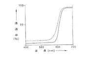
この際の着色画素の分光透過率は、例えば、図5における実線で示すように、赤色の着色画素の分光透過率は波長400〜600nmにおいては透過率が低く、波長600〜700nmにおいては透過率が高いものが好ましいものである。
In the transmissive liquid crystal display device, light from a backlight provided behind the transmissive liquid crystal display device passes through the colored pixels of the color filter and is emitted to the outside in front of the liquid crystal display device being viewed. .
At this time, the spectral transmittance of the colored pixel is, for example, as shown by a solid line in FIG. 5, the spectral transmittance of the red colored pixel is low at a wavelength of 400 to 600 nm and low at a wavelength of 600 to 700 nm. A high value is preferable.
図6は、従来法の反射型液晶表示装置の一例を断面で示す説明図であるが、図6に示すように、反射型液晶表示装置(60)は、対向基板(68)、液晶(65)、カラーフィルタ(69)などで構成されている。図6において、対向基板(68)は、画素表示に必要な駆動素子(図示せず)や光拡散反射性の電極層(66)などが基板(67)上に形成されたもので構成されている。
また、カラーフィルタ(69)は、ガラス基板(61)、着色画素(62)、オーバーコート層(63)、透明電極層(64)などで構成されている。
FIG. 6 is an explanatory view showing an example of a reflection type liquid crystal display device of a conventional method in cross section. As shown in FIG. 6, the reflection type liquid crystal display device (60) includes a counter substrate (68), a liquid crystal (65 ), A color filter (69), and the like. In FIG. 6, a counter substrate (68) is configured by a driving element (not shown) necessary for pixel display, a light diffusive reflective electrode layer (66), and the like formed on a substrate (67). Yes.
The color filter (69) includes a glass substrate (61), a colored pixel (62), an overcoat layer (63), a transparent electrode layer (64), and the like.
図6において、外光(L1)は着色画素(62)を通過し色光となり、光拡散反射性の電極層(66)にて反射され、再び着色画素(62)を通過して、外部へ反射光(L2)として射出されるようになっている。
このような反射型液晶表示装置用カラーフィルタの着色画素(62)の色濃度は、透過型液晶表示装置用カラーフィルタのカラーフィルタ画素の色濃度より低い色濃度のものである。
In FIG. 6, the external light (L1) passes through the colored pixel (62) to become colored light, is reflected by the light diffusion reflective electrode layer (66), passes through the colored pixel (62) again, and is reflected to the outside. The light (L2) is emitted.
The color density of the colored pixel (62) of the color filter for the reflective liquid crystal display device is lower than the color density of the color filter pixel of the color filter for the transmissive liquid crystal display device.
これは、上記のように外部からの光は、入射の際と反射の際の2回にわたり赤色の着色画素を透過し、外部へ射出されるので、例えば、図5における点線で示すように、赤色の着色画素の分光透過率は波長400〜600nmにおいて透過率がやや高く、波長600〜700nmにおいても透過率がやや高いものを用いることにより、実線で示す透過型に用いられる赤色の着色画素の分光透過率と同様の効果が得られるようにしているのである。
そして、このような点線で示す分光透過率を有する着色画素の形成は、例えば、着色画素に含まれる顔料の含有量を少なくすることにより行われている。
This is because, as described above, light from the outside passes through the red colored pixel twice and is emitted to the outside at the time of incidence and reflection, for example, as shown by the dotted line in FIG. The spectral transmittance of the red colored pixel is slightly higher at a wavelength of 400 to 600 nm and slightly higher at a wavelength of 600 to 700 nm, so that the red colored pixel used in the transmission type indicated by the solid line is used. The same effect as the spectral transmittance is obtained.
And formation of the colored pixel which has such a spectral transmittance shown with a dotted line is performed by reducing content of the pigment contained in a colored pixel, for example.
さて、液晶表示装置用カラーフィルタの着色画素の形成は、種々な方法により行われているが、感光性樹脂組成物に顔料を分散させた感光性着色樹脂組成物(着色フォトレジスト)を材料として用い、フォトリソグラフィー法により着色画素を形成する顔料分散法が広く採用されている。 The colored pixels of the color filter for a liquid crystal display device are formed by various methods. A photosensitive colored resin composition (colored photoresist) in which a pigment is dispersed in the photosensitive resin composition is used as a material. A pigment dispersion method in which colored pixels are formed by photolithography is widely used.
この顔料分散法、すなわち、着色フォトレジストを用いフォトリソグラフィー法により、上記のような反射型液晶表示装置用カラーフィルタの着色画素を形成する場合には、画素の色濃度を低くするため、その着色画素に含まれる顔料の含有量を少なくしたり、または、着色画素の厚さを薄く形成する手段が用いられている。 In the case of forming the colored pixels of the color filter for the reflective liquid crystal display device as described above by this pigment dispersion method, that is, by photolithography using a colored photoresist, the coloring is performed in order to reduce the color density of the pixels. Means for reducing the content of the pigment contained in the pixel or reducing the thickness of the colored pixel is used.
上記透過型液晶表示装置は、主に屋内のような暗い環境下で用いられるものであり、屋外のような周囲が明るい環境下では、その表示が見にくいといった欠点がある。また、上記反射型液晶表示装置は、主に屋外のような周囲が明るい環境下で用いられるものであり、屋内のような暗い環境下では、その表示が見にくいといった欠点がある。 The transmissive liquid crystal display device is mainly used in a dark environment such as indoors, and has a drawback that its display is difficult to see in a bright environment such as outdoors. The reflective liquid crystal display device is mainly used in a bright environment such as outdoors, and has a drawback that its display is difficult to see in a dark environment such as indoors.
このような透過型液晶表示装置、反射型液晶表示装置に対し、半透過型液晶表示装置と称される液晶表示装置は、1基の液晶表示装置において透過型と反射型の両機能を兼ね備えた液晶表示装置である。
この半透過型液晶表示装置は、屋外のような非常に明るい環境下でも、屋内のような暗い環境下でも用いることができるものであり、モバイル機器に用いられる液晶表示装置である。
In contrast to such a transmissive liquid crystal display device and a reflective liquid crystal display device, a liquid crystal display device called a transflective liquid crystal display device has both functions of a transmissive type and a reflective type in one liquid crystal display device. It is a liquid crystal display device.
This transflective liquid crystal display device can be used in a very bright environment such as outdoors or in a dark environment such as indoors, and is a liquid crystal display device used in mobile devices.
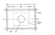
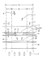
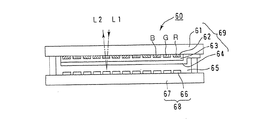
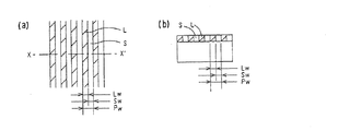
図3は、半透過型液晶表示装置に用いられるカラーフィルタの一例を示したものであり、特に、一画素に対応する部位を拡大して示す平面図である。また、図4は、図3に示す半透過型液晶表示装置用カラーフィルタを用いた半透過型液晶表示装置の一画素の部分を示す断面説明図である。図3におけるX−X’線の断面が、図4に示す半透過型液晶表示装置用カラーフィルタ(30)の断面に相当する。 FIG. 3 shows an example of a color filter used in a transflective liquid crystal display device, and in particular, is a plan view showing an enlarged portion corresponding to one pixel. FIG. 4 is a cross-sectional explanatory view showing a pixel portion of a transflective liquid crystal display device using the color filter for the transflective liquid crystal display device shown in FIG. The cross section taken along the line X-X ′ in FIG. 3 corresponds to the cross section of the color filter (30) for the transflective liquid crystal display device shown in FIG.
図3、及び図4に示すように、この半透過型液晶表示装置は、半透過型液晶表示装置用カラーフィルタ(30)、半透過型液晶表示装置用カラーフィルタ上に形成された透明電極(14)、液晶(50)、TFT素子(図示せず)などが形成されたTFT基板(40)、TFT基板上に形成された透明電極(41)及び反射電極(42)で構成されている。 As shown in FIGS. 3 and 4, the transflective liquid crystal display device includes a translucent liquid crystal display device color filter (30) and a transparent electrode (30) formed on the transflective liquid crystal display device color filter. 14), a liquid crystal (50), a TFT substrate (40) on which a TFT element (not shown) and the like are formed, a transparent electrode (41) and a reflective electrode (42) formed on the TFT substrate.
半透過型液晶表示装置用カラーフィルタ(30)は、ガラス基板(11)上にブラックマトリックス(12)、着色画素(13)が形成されたものである。また、透明電極(41)及び反射電極(42)はTFT素子のドレイン電極と接続されている。 The color filter (30) for a transflective liquid crystal display device has a black matrix (12) and colored pixels (13) formed on a glass substrate (11). The transparent electrode (41) and the reflective electrode (42) are connected to the drain electrode of the TFT element.
1画素の領域(Px)はブラックマトリックス(12)を除くと、光透過領域(Tr)と光反射領域(Re)とで構成されている。 Except for the black matrix (12), one pixel region (Px) is composed of a light transmission region (Tr) and a light reflection region (Re).
光透過領域(Tr)は、透過型液晶表示装置として機能する領域であり、光反射領域(Re)は、反射型液晶表示装置として機能する領域である。 The light transmissive region (Tr) is a region that functions as a transmissive liquid crystal display device, and the light reflective region (Re) is a region that functions as a reflective liquid crystal display device.
1画素の領域(Px)内の着色層(15)及び透明部を有する着色層(16)は、同一の着色層形成材料を用いて設けられた同一厚さの着色層である。図4にては、説明上、左斜線と右斜線で表記してある。また、図4中、反射電極(42)の両端の上方が着色層(15)と透明部を有する着色層(16)との境界であり、鎖線で表記してある。
着色画素(13)の光透過領域(Tr)には、その全領域に厚さD1の均一な着色層(15)が形成され、また、光反射領域(Re)には、外光が入反射する透明部(スルーホー
ル部)(17)を有する着色層(16)が形成されている。
The colored layer (15) in the one pixel region (Px) and the colored layer (16) having a transparent portion are colored layers having the same thickness provided using the same colored layer forming material. In FIG. 4, for the sake of explanation, the left diagonal line and the right diagonal line are used. Moreover, in FIG. 4, the upper part of both ends of the reflective electrode (42) is a boundary between the colored layer (15) and the colored layer (16) having a transparent portion, and is indicated by a chain line.
In the light transmission region (Tr) of the colored pixel (13), a uniform colored layer (15) having a thickness D1 is formed in the entire region, and external light enters and reflects in the light reflection region (Re). A colored layer (16) having a transparent part (through hole part) (17) to be formed is formed.
すなわち、1画素の領域(Px)内では、光透過領域(Tr)の均一な着色層(15)と、光反射領域(Re)の透明部を有する着色層(16)とで着色画素(13)が構成されている。
そして、この透明部を有する着色層(16)の厚さは、その平均厚さ(D2)で表される。尚、平坦性をもたせるため着色層(16)の透明部(スルーホール部)(17)には、無色透明な樹脂を充填するのが一般的である。
That is, in the region (Px) of one pixel, the colored pixel (13) is composed of a uniform colored layer (15) in the light transmitting region (Tr) and a colored layer (16) having a transparent portion in the light reflecting region (Re). ) Is configured.
And the thickness of the colored layer (16) which has this transparent part is represented by the average thickness (D2). In order to provide flatness, the transparent portion (through hole portion) (17) of the colored layer (16) is generally filled with a colorless and transparent resin.
図4に示す、厚さD1を有する均一な着色層(15)の分光透過率は図5に実線で示すような、例えば、赤色の着色画素の分光透過率は波長400〜600nmにおいては透過率が低く、波長600〜700nmにおいては透過率が高い透過型液晶表示装置に好適な分光透過率を有する。
光透過領域(Tr)においては白太矢印(A)で示すバックライトからの白色光が、TFT基板(40)、透明電極(41)、液晶(50)、透明電極(14)を経て着色画素(13)の光透過領域(Tr)の着色層(15)を通過し色光となり白細矢印(a)で示すように、外部へ射出するようになっている。
従って、この半透過型液晶表示装置のバックライトを点灯し透過型液晶表示装置として使用した際には、透過型液晶表示装置として優れた明度、彩度を有する透過カラー表示をする。
The spectral transmittance of the uniform colored layer (15) having the thickness D1 shown in FIG. 4 is shown by the solid line in FIG. 5, for example, the spectral transmittance of the red colored pixel is the transmittance at a wavelength of 400 to 600 nm. And a spectral transmittance suitable for a transmissive liquid crystal display device having a high transmittance at a wavelength of 600 to 700 nm.
In the light transmission region (Tr), white light from the backlight indicated by the white thick arrow (A) passes through the TFT substrate (40), the transparent electrode (41), the liquid crystal (50), and the transparent electrode (14), and is colored pixels. It passes through the colored layer (15) in the light transmission region (Tr) of (13) and becomes colored light, and is emitted to the outside as indicated by a white arrow (a).
Therefore, when the backlight of this transflective liquid crystal display device is turned on and used as a transmissive liquid crystal display device, a transmissive color display having excellent brightness and saturation as the transmissive liquid crystal display device is obtained.
また、この半透過型液晶表示装置のバックライトを消灯し、屋外のような非常に明るい環境下で反射型液晶表示装置として使用した際には、光反射領域(Re)において、斜線太矢印(B)で示す周囲からの外光が、ガラス基板(11)、平均厚さ(D2)の、透明部を有する着色層(16)を通過し色光となり反射電極(42)にて反射され、斜線細矢印(b)で示すように、再び外部へ射出するようになっている。 Further, when the backlight of this transflective liquid crystal display device is turned off and used as a reflective liquid crystal display device in a very bright environment such as outdoors, a hatched thick arrow ( The external light from the surrounding shown by B) passes through the colored layer (16) having the transparent portion of the glass substrate (11) and the average thickness (D2), becomes colored light, is reflected by the reflective electrode (42), and is shaded. As indicated by the thin arrow (b), the liquid is again injected to the outside.
この際の反射光は、平均厚さ(D2)の透明部を有する着色層(16)を2回にわたり通過しているので、その分光透過率は図5に点線で示すような、赤色の着色画素の分光透過率は波長400〜600nmにおいて透過率がかなり高く、波長600〜700nmにおいても透過率が高い、すなわち、反射型液晶表示装置の分光透過率として好適な分光透過率を有するものとなる。 Since the reflected light at this time has passed through the colored layer (16) having a transparent portion having an average thickness (D2) twice, its spectral transmittance is colored red as shown by a dotted line in FIG. The spectral transmittance of the pixel is quite high at a wavelength of 400 to 600 nm and high at a wavelength of 600 to 700 nm, that is, has a spectral transmittance suitable as the spectral transmittance of a reflective liquid crystal display device. .
このような半透過型液晶表示装置用カラーフィルタを用いることにより、透過型液晶表示装置としての優れた明度、彩度を有する透過カラー表示をし、また、反射型液晶表示装置として暗くならず、優れた明度、彩度を有する反射カラー表示をすることが可能となる。 By using such a color filter for a transflective liquid crystal display device, a transmissive color display having excellent brightness and saturation as a transmissive liquid crystal display device is obtained, and it is not dark as a reflective liquid crystal display device. Reflective color display having excellent brightness and saturation can be achieved.
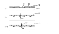
図2は、上述した半透過型液晶表示装置用カラーフィルタを製造する従来の方法の一例の説明図である。この方法は、図2(a)に示すように、先ず、ブラックマトリックス(12)が形成されたガラス基板(11)上に、着色層(25)を形成し、次に、図2(b)に示すように、着色層(25)が形成されたガラス基板(11)上の全面に、透明な光硬化性樹脂(22)を塗布し、全面に露光を与え、透明部(スルーホール部)(27)に透明樹脂を充填する方法である。 FIG. 2 is an explanatory diagram showing an example of a conventional method for manufacturing the above-described color filter for a transflective liquid crystal display device. In this method, as shown in FIG. 2 (a), first, a colored layer (25) is formed on a glass substrate (11) on which a black matrix (12) is formed, and then, FIG. 2 (b). As shown in FIG. 2, a transparent photo-curing resin (22) is applied to the entire surface of the glass substrate (11) on which the colored layer (25) is formed, and the entire surface is exposed to light, whereby a transparent portion (through hole portion) (27) is a method of filling a transparent resin.
しかし、この方法によると、ガラス基板(11)上には着色層(25)が形成されていない部分と、着色層(25)が形成されている部分に着色層(25)の厚さに相当する段差(D3)があるために、例えば、スピンナーで透明な光硬化性樹脂(22)を塗布すると、図2(b’)に示すように、透明部(スルーホール部)(27)に充填した光硬化性樹脂(22)の表面は平坦にならず、窪み(23)が生じたものとなりやすい。 However, according to this method, the thickness of the colored layer (25) corresponds to the portion where the colored layer (25) is not formed on the glass substrate (11) and the portion where the colored layer (25) is formed. Since there is a step (D3) to be applied, for example, when a transparent photocurable resin (22) is applied with a spinner, the transparent portion (through hole portion) (27) is filled as shown in FIG. The surface of the cured photocurable resin (22) does not become flat and tends to have a depression (23).
この窪み(23)の深さ(D4)は、厚み1.2μm程度の着色層(25)に、厚さ1.95μm程度の光硬化性樹脂(22)を形成した際に0.2μm程度となる。表面に窪みが生じたカラーフィルタは、液晶表示装置に用いた際に、窪みのセルギャップが局所的に広くなり、表示ムラを生じる場合があり好ましいものではない。 The depth (D4) of the depression (23) is about 0.2 μm when the photocurable resin (22) having a thickness of about 1.95 μm is formed on the colored layer (25) having a thickness of about 1.2 μm. Become. When used in a liquid crystal display device, a color filter having a depression on the surface is not preferable because the cell gap of the depression is locally widened and display unevenness may occur.
従って、透明部(27)の表面を平坦に充填する方法としては、例えば、図7(a)〜(f)に示す方法がとられる場合がある。
すなわち、先ず、ブラックマトリックス(12)が形成されたガラス基板(11)上に、ネガ型無色透明フォトレジスト(78)を塗布し、透明部(17)を光透過させるフォトマスク(PM3)を介して露光(C)、現像処理を行い、透明部(17)を形成する(図7(a)〜(c))。
Therefore, as a method of filling the surface of the transparent portion (27) flatly, for example, the methods shown in FIGS. 7A to 7F may be used.
That is, first, a negative colorless transparent photoresist (78) is applied on the glass substrate (11) on which the black matrix (12) is formed, and the photomask (PM3) through which light passes through the transparent portion (17). Then, exposure (C) and development processing are performed to form a transparent portion (17) (FIGS. 7A to 7C).
次に、透明部が形成されたガラス基板(11)上に、ネガ型着色フォトレジスト(79)を塗布し、着色層の部分を光透過させるフォトマスク(PM4)を介して露光(C)、現像処理を行い、着色層(15)を形成し、均一な着色層(15)と透明部を有する着色層(16)とで構成される着色画素(13)を形成するといった方法である。(図7(d)〜(f))
この方法によれば、透明部(17)の厚さと着色層(15)の厚さが同一で窪みのない、表面が面一な、すなわち、表面が平坦な着色画素を有するカラーフィルタが得られる。
Next, a negative colored photoresist (79) is applied on the glass substrate (11) on which the transparent portion is formed, and exposure (C) is performed through a photomask (PM4) that transmits light through the colored layer. A development process is performed to form a colored layer (15), and a colored pixel (13) composed of a uniform colored layer (15) and a colored layer (16) having a transparent portion is formed. (FIGS. 7D to 7F)
According to this method, it is possible to obtain a color filter having colored pixels in which the thickness of the transparent portion (17) and the thickness of the colored layer (15) are the same and there is no depression and the surface is flush, that is, the surface is flat. .
しかし、この方法は、透明部の部分を光透過させるフォトマスク(PM3)と着色層の部分を光透過させるフォトマスク(PM4)の2枚のフォトマスクを使用するので、カラーフィルタを製造する際のガラス基板が大型の場合などには、透明部を有する着色層(16)の透明部(17)と着色層部分の境界(E)の位置関係を精度よく合わせて製造するのは困難であり、境界(E)には、着色層部分が透明部に重なった角(ツノ)や隙間が発生し、液晶の配向に悪影響を及ぼすこととなる。
本発明は、上記問題を解決するためになされたものであり、着色画素が光透過領域に形成された着色層と、光反射領域に形成され、透明部(スルーホール部)を有する着色層とで構成される半透過型液晶表示装置用カラーフィルタの製造において、表面が平坦で、着色層中の透明部(スルーホール部)と着色層部分の位置精度の優れたカラーフィルタを廉価に、容易に製造することのできる半透過型液晶表示装置用カラーフィルタの製造方法を提供することを課題とするものである。
また、本発明は、上記半透過型液晶表示装置用カラーフィルタを提供することを課題とする。
The present invention has been made to solve the above problems, and a colored layer in which colored pixels are formed in a light transmission region, and a colored layer having a transparent portion (through hole portion) formed in a light reflection region, In manufacturing color filters for transflective liquid crystal display devices, it is easy to inexpensively and easily produce color filters that have a flat surface and a transparent portion (through-hole portion) in the colored layer and excellent positional accuracy of the colored layer portion. It is an object of the present invention to provide a method of manufacturing a color filter for a transflective liquid crystal display device that can be manufactured easily.
Another object of the present invention is to provide a color filter for the transflective liquid crystal display device.
本発明は、一画素中の着色画素が、光透過領域に形成された着色層と、光反射領域に形成され、透明部を有する着色層とで構成される半透過型液晶表示装置用カラーフィルタの製造方法において、
1)基板上に着色フォトレジストを用いて着色画素を形成し、
2)着色画素が形成された基板上の全面に無色透明フォトレジストを塗布し、
3)着色画素の厚さに、着色画素上に形成される無色透明樹脂層の厚さを加算した厚さ(D8)を、透明部に充填される無色透明樹脂層の厚さ(D5)と同一に形成するためのハーフトーン部を有するフォトマスクを介して露光し、現像処理を行い、
透明部に充填された無色透明樹脂層の表面と着色画素上に形成された無色透明樹脂層の表面とが面一で平坦なカラーフィルタを製造することを特徴とする半透過型液晶表示装置用カラーフィルタの製造方法である。
The present invention relates to a color filter for a transflective liquid crystal display device, wherein a colored pixel in one pixel is composed of a colored layer formed in a light transmission region and a colored layer formed in a light reflection region and having a transparent portion. In the manufacturing method of
1) A colored pixel is formed on a substrate using a colored photoresist,
2) Apply a colorless and transparent photoresist on the entire surface of the substrate on which the colored pixels are formed,
3) The thickness (D8) obtained by adding the thickness of the colorless transparent resin layer formed on the colored pixel to the thickness of the colored pixel is referred to as the thickness (D5) of the colorless transparent resin layer filled in the transparent portion. Exposure through a photomask having a halftone portion for the same formation, development processing,
A transflective liquid crystal display device characterized by producing a color filter in which a surface of a colorless transparent resin layer filled in a transparent portion and a surface of a colorless transparent resin layer formed on a colored pixel are flush with each other. It is a manufacturing method of a color filter.
また、本発明は、前記ハーフトーン部がクロム膜、金属酸化膜、又はラインアンドスペースパターンであることを特徴とする半透過型液晶表示装置用カラーフィルタの製造方法である。 The present invention is also the method of manufacturing a color filter for a transflective liquid crystal display device, wherein the halftone portion is a chromium film, a metal oxide film, or a line and space pattern.
また、本発明は、請求項1又は請求項2記載の半透過型液晶表示装置用カラーフィルタの製造方法を用いて製造したことを半透過型液晶表示装置用カラーフィルタである。
In addition, the present invention is a color filter for a transflective liquid crystal display device manufactured using the method for manufacturing a color filter for a transflective liquid crystal display device according to
本発明は、一画素中の着色画素が、光透過領域に形成された着色層と、光反射領域に形成され、透明部を有する着色層とで構成される半透過型液晶表示装置用カラーフィルタの製造方法において、基板上に着色フォトレジストを用いて着色画素を形成し、着色画素が形成された基板上の全面に無色透明フォトレジストを塗布し、着色画素の厚さに、着色画素上に形成される無色透明樹脂層の厚さを加算した厚さを、透明部に充填される無色透明樹脂層の厚さと同一に形成するためのハーフトーン部を有するフォトマスクを介して露光し、現像処理を行い、半透過型液晶表示装置用カラーフィルタを製造する方法であるので、透明部に充填された無色透明樹脂層の表面と着色画素上に形成された無色透明樹脂層の表面とが面一で平坦で、着色層中の該透明部(スルーホール部)と着色層部分の位置精度の優れたカラーフィルタを廉価に、容易に製造することのできる半透過型液晶表示装置用カラーフィルタの製造方法となる。 The present invention relates to a color filter for a transflective liquid crystal display device, wherein a colored pixel in one pixel is composed of a colored layer formed in a light transmission region and a colored layer formed in a light reflection region and having a transparent portion. In this manufacturing method, a colored pixel is formed on a substrate using a colored photoresist, a colorless transparent photoresist is applied to the entire surface of the substrate on which the colored pixel is formed, and the thickness of the colored pixel is set on the colored pixel. The thickness obtained by adding the thickness of the colorless and transparent resin layer to be formed is exposed through a photomask having a halftone portion to form the same thickness as the colorless and transparent resin layer filled in the transparent portion, and developed. Since the process is a method for producing a color filter for a transflective liquid crystal display device, the surface of the colorless and transparent resin layer filled in the transparent portion and the surface of the colorless and transparent resin layer formed on the colored pixels are surfaces. One flat and colored layer Excellent color filter inexpensively, a method of manufacturing a transflective color filter for a liquid crystal display device which can be easily produced in the positional accuracy of the colored layer portion and the transparent portion (through hole portion).
以下に本発明による半透過型液晶表示装置用カラーフィルタの製造方法を、その一実施形態に基づいて説明する。 Hereinafter, a method for producing a color filter for a transflective liquid crystal display device according to the present invention will be described based on an embodiment thereof.
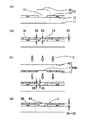
図1(a)〜(d)は、本発明による半透過型液晶表示装置用カラーフィルタの製造方法の一実施例を示す断面図である。図1は、半透過型液晶表示装置用カラーフィルタを構成する一画素中の着色画素部分の断面を拡大して示すものである。 1A to 1D are cross-sectional views showing an embodiment of a method for producing a color filter for a transflective liquid crystal display device according to the present invention. FIG. 1 is an enlarged view of a cross section of a colored pixel portion in one pixel constituting a color filter for a transflective liquid crystal display device.
図1(d)に示すように、本発明による半透過型液晶表示装置用カラーフィルタの製造方法は、例えば、ブラックマトリックス(12)が形成されたガラス基板(11)上に、光透過領域に形成される着色層(15)と、光反射領域に形成され透明部を有する着色層(16)とで構成される着色画素(13)を有し、透明部に充填された無色透明樹脂層の表面(8A)と着色画素上に形成された無色透明樹脂層の表面(8B)とが面一で平坦なカラーフィルタを製造する方法である。 As shown in FIG.1 (d), the manufacturing method of the color filter for transflective liquid crystal display devices by this invention is the light transmission area | region on the glass substrate (11) in which the black matrix (12) was formed, for example. A colorless transparent resin layer having a colored pixel (13) composed of a colored layer (15) to be formed and a colored layer (16) formed in a light reflection region and having a transparent portion, and filled in the transparent portion. This is a method for producing a color filter in which the surface (8A) and the surface (8B) of the colorless transparent resin layer formed on the colored pixels are flush with each other.
先ず、ブラックマトリックス(12)が形成されたガラス基板(11)上に、ネガ型の着色フォトレジストを塗布し、着色画素(13)部を光透過させるフォトマスクを介した露光、現像、バーニングを行い着色画素(13)を形成する。
着色画素(13)は、着色層(15)と、透明部(17)を有する着色層(16)とで構成されている。図1(a)は着色画素(13)が形成された段階のものである。
First, a negative colored photoresist is applied on a glass substrate (11) on which a black matrix (12) is formed, and exposure, development, and burning are performed through a photomask that transmits light through the colored pixel (13) portion. A colored pixel (13) is formed.
The colored pixel (13) is composed of a colored layer (15) and a colored layer (16) having a transparent portion (17). FIG. 1A shows the stage where the colored pixels (13) are formed.
次に、図1(b)に示すように、着色画素(13)が形成されたガラス基板(11)上の全面に無色透明フォトレジスト(18)を塗布する。ガラス基板(11)上には既に着色画素(13)が形成されているので、ガラス基板(11)上の全面に無色透明フォトレジスト(18)を塗布すると、透明部上に塗布された無色透明フォトレジスト(18)のガラス基板(11)からの厚さ(D5)は、着色画素(13)の厚さに、着色画素(13
)上に塗布された無色透明フォトレジスト(18)の厚さを加算した厚さ(D6)より薄いものとなり、窪み(23)が生じる。尚、符号(D7)は窪み(23)の深さを表している(D7=D6−D5)。
Next, as shown in FIG.1 (b), a colorless transparent photoresist (18) is apply | coated to the whole surface on the glass substrate (11) in which the colored pixel (13) was formed. Since the colored pixels (13) are already formed on the glass substrate (11), when the colorless and transparent photoresist (18) is applied to the entire surface of the glass substrate (11), the colorless and transparent applied on the transparent portion. The thickness (D5) of the photoresist (18) from the glass substrate (11) is the same as that of the colored pixel (13).
) The thickness (D6) obtained by adding the thickness of the colorless and transparent photoresist (18) applied thereon is thinner, and the depression (23) is generated. Reference numeral (D7) represents the depth of the recess (23) (D7 = D6-D5).
次に、図1(c)に示すように、フォトマスク(PM1)を介した露光(C)を行う。フォトマスク(PM1)は、透明基板(40)に、ハーフトーン部(1)、フォトマスク透明部(2)が設けられたものである。
ハーフトーン部(1)は、着色画素(13)の厚さに、着色画素(13)上に形成される無色透明樹脂層の厚さを加算した厚さ(D8)を、透明部(17)に充填される無色透明樹脂層の厚さ(D5)と同一に形成するためのハーフトーン部である。フォトマスク透明部(2)は、透明部(17)に充填される無色透明樹脂層の形成に対応したフォトマスク透明部である。
Next, as shown in FIG. 1C, exposure (C) through a photomask (PM1) is performed. The photomask (PM1) is a transparent substrate (40) provided with a halftone part (1) and a photomask transparent part (2).
The halftone part (1) has a thickness (D8) obtained by adding the thickness of the colorless transparent resin layer formed on the colored pixel (13) to the thickness of the colored pixel (13), and the transparent part (17). It is a halftone portion for forming the same as the thickness (D5) of the colorless and transparent resin layer filled in the. The photomask transparent part (2) is a photomask transparent part corresponding to the formation of a colorless transparent resin layer filled in the transparent part (17).
ハーフトーン部(1)の光学濃度は、着色画素(13)上に形成される無色透明樹脂層の形成に対応した光学濃度を有し、透明部(2)の光学濃度はゼロである。このようなフォトマスク(PM1)は、例えば、透明基板(40)上に成膜されたクロム膜をフォトエッチングすることによって得られる。尚、図1中にては、光学濃度の高さを各部の厚みで模式的に表している。 The optical density of the halftone part (1) has an optical density corresponding to the formation of the colorless transparent resin layer formed on the colored pixel (13), and the optical density of the transparent part (2) is zero. Such a photomask (PM1) can be obtained, for example, by photoetching a chromium film formed on the transparent substrate (40). In FIG. 1, the height of the optical density is schematically represented by the thickness of each part.
図1(c)に示すように、フォトマスク(PM1)の上方からの、白太矢印で示す紫外光はフォトマスクの全域を均一に照射されるが、透明部(2)では略その全量が透過し、ハーフトーン部(1)では、その光学濃度に応じた白細矢印で示す紫外光が透過することになる。
その光学濃度は、着色画素(13)上に形成される無色透明樹脂層の厚さと、着色画素(13)の厚さを加算した厚さ(D8)が、透明部(17)に充填される無色透明樹脂層の厚さ(D5)と同一になるような厚さの無色透明樹脂層を着色画素(13)上に形成する光学濃度である。
As shown in FIG. 1C, the ultraviolet light indicated by the white thick arrow from above the photomask (PM1) is uniformly irradiated over the entire area of the photomask. In the halftone portion (1), ultraviolet light indicated by white thin arrows corresponding to the optical density is transmitted.
As for the optical density, the transparent portion (17) is filled with a thickness (D8) obtained by adding the thickness of the colorless transparent resin layer formed on the colored pixel (13) and the thickness of the colored pixel (13). This is the optical density at which a colorless transparent resin layer having the same thickness as the colorless transparent resin layer (D5) is formed on the colored pixels (13).
従って、図1(d)に示すように、露光後の現像処理によって得られる、透明部に充填された無色透明樹脂層の表面(8A)と、着色画素上に形成された無色透明樹脂層の表面(8B)とが面一で平坦なカラーフィルタとなる。
また、得られた着色画素(13)と透明部(17)の境界(E)には、着色層部分が透明部に重なった角(ツノ)や隙間は生じない。
Accordingly, as shown in FIG. 1 (d), the surface (8A) of the colorless transparent resin layer filled in the transparent portion obtained by the development processing after exposure, and the colorless transparent resin layer formed on the colored pixels The surface (8B) is flush with the flat color filter.
In addition, at the boundary (E) between the obtained colored pixel (13) and the transparent portion (17), there are no corners (horns) or gaps where the colored layer portion overlaps the transparent portion.
図8は、本発明における、平坦な表面を形成するためのハーフトーン部を有するフォトマスクの第2例を説明する断面図である。
図8に示すように、第2例のフォトマスク(PM2A)は、透明基板(40)に、紫外光を減衰させる薄膜、例えば、ITOなどの金属酸化物膜からなるハーフトーン部(1A)、紫外光の略全量が透過する透明部(2)が設けられたものである。
FIG. 8 is a cross-sectional view illustrating a second example of a photomask having a halftone portion for forming a flat surface in the present invention.
As shown in FIG. 8, the photomask (PM2A) of the second example has a transparent substrate (40) with a halftone portion (1A) made of a thin film that attenuates ultraviolet light, for example, a metal oxide film such as ITO, A transparent portion (2) through which substantially the entire amount of ultraviolet light is transmitted is provided.
ハーフトーン部(1A)の膜厚は、前記着色画素(13)上の無色透明樹脂層)の形成に応じた紫外光の強度となるように設定される。
この第2例に示すフォトマスク(PM2A)を用いることによって、図1に示す例と同様に、着色画素(13)が形成されたガラス基板(11)上に、透明部に充填された無色透明樹脂層の表面(8A)と、着色画素上に形成された無色透明樹脂層の表面(8B)とが面一で平坦なカラーフィルタとなる。
The film thickness of the halftone portion (1A) is set so that the intensity of the ultraviolet light corresponds to the formation of the colorless transparent resin layer on the colored pixel (13).
By using the photomask (PM2A) shown in the second example, the transparent portion is colorless and transparent filled on the glass substrate (11) on which the colored pixels (13) are formed as in the example shown in FIG. The surface (8A) of the resin layer and the surface (8B) of the colorless and transparent resin layer formed on the colored pixels form a flat color filter that is flush with the surface.
図9は、本発明における、平坦な表面を形成するためのハーフトーン部を有するフォトマスクの第3例を説明する断面図である。
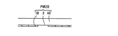
図9に示すように、第3例のフォトマスク(PM2B)は、透明基板(40)に、ライン
アンドスペースパターンからなるハーフトーン部(1B)、紫外光の略全量が透過する透明部(2)が設けられたものである。
FIG. 9 is a cross-sectional view for explaining a third example of a photomask having a halftone portion for forming a flat surface in the present invention.
As shown in FIG. 9, the photomask (PM2B) of the third example has a transparent substrate (40) with a halftone portion (1B) made of a line-and-space pattern and a transparent portion (2 that transmits almost the entire amount of ultraviolet light). ) Is provided.
ハーフトーン部(1B)のラインアンドスペースパターンは、前記着色画素(13)上の無色透明樹脂層の形成に応じた紫外光を透過するように設定される。
この第3例に示すフォトマスク(PM2B)を用いることによって、図1に示す例と同様に、着色画素(13)が形成されたガラス基板(11)上に、透明部に充填された無色透明樹脂層の表面(8A)と、着色画素上に形成された無色透明樹脂層の表面(8B)とが面一で平坦なカラーフィルタとなる。
The line and space pattern of the halftone portion (1B) is set so as to transmit ultraviolet light according to the formation of the colorless transparent resin layer on the colored pixel (13).
By using the photomask (PM2B) shown in the third example, the transparent portion filled with a transparent portion is formed on the glass substrate (11) on which the colored pixels (13) are formed, as in the example shown in FIG. The surface (8A) of the resin layer and the surface (8B) of the colorless and transparent resin layer formed on the colored pixels form a flat color filter that is flush with the surface.
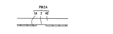
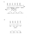
図10(a)は、図9に示すハーフトーン部(1B)の一部分を拡大して示す平面図である。また、図10(b)は、図10(a)におけるX−X’線の断面図である。図10(a)、(b)に示すように、このハーフトーン部(1B)は光を遮光するライン(L)と光を透過するスペース(S)で構成されるラインアンドスペースパターンである。 FIG. 10A is an enlarged plan view showing a part of the halftone portion (1B) shown in FIG. FIG. 10B is a cross-sectional view taken along line X-X ′ in FIG. As shown in FIGS. 10A and 10B, this halftone portion (1B) is a line-and-space pattern composed of a line (L) that blocks light and a space (S) that transmits light.
本発明における第3例のフォトマスク(PM2B)は、このフォトマスク上のハーフトーン部(1B)のラインアンドスペースパターンが、用いるフォトリソグラフィー法の系の解像度以下となっているフォトマスクである。
フォトリソグラフィー法の系とは、無色透明樹脂層を形成する際の光学系、フォトマスク、無色透明フォトレジスト、現像処理などのプロセス全体を指し、得られる無色透明樹脂層のパターンの解像度は、この系の解像度によって定まる。
The photomask (PM2B) of the third example in the present invention is a photomask in which the line and space pattern of the halftone portion (1B) on this photomask is below the resolution of the system of the photolithography method used.
The photolithographic method system refers to the entire process of forming the colorless and transparent resin layer, such as the optical system, photomask, colorless and transparent photoresist, and development processing. The resolution of the pattern of the resulting colorless and transparent resin layer is It depends on the resolution of the system.
例えば、露光光の位相のそろい度合い、フォトマスクを縮小投影して用いる場合と、原寸にて用いる場合、或いはフォトマスクの構造形式によりフォトマスクの実効解像度の相違、原寸露光におけるプロキシミティ量、或いは無色透明フォトレジストの解像度、現像処理条件などによって系の解像度が定まる。
本発明においては、1枚のフォトマスクを介した露光によって、着色画素の厚さに、着色画素上に形成される無色透明樹脂層の厚さを加算した厚さ(D8)を、透明部に充填される無色透明樹脂層の厚さ(D5)と同一に、且つ平坦に形成するために、フォトマスク上のハーフトーン部(1B)のラインアンドスペースパターンを、無色透明フォトレジストへの露光時において、そのフォトリソグラフィー法の系の解像度以下とする。
For example, the degree of phase alignment of the exposure light, the case where the photomask is used after being projected at a reduced size, and the case where the photomask is used in its original size, or the difference in effective resolution of the photomask depending on the structure type of the photomask, The resolution of the system is determined by the resolution of the colorless transparent photoresist, development processing conditions, and the like.
In the present invention, the thickness (D8) obtained by adding the thickness of the colorless transparent resin layer formed on the colored pixel to the thickness of the colored pixel by exposure through one photomask is added to the transparent portion. The line-and-space pattern of the halftone portion (1B) on the photomask is exposed to the colorless and transparent photoresist in order to form a flat and uniform thickness (D5) of the colorless and transparent resin layer to be filled. In the above, the resolution is set to be equal to or lower than the resolution of the photolithography system.
図11は、図10(b)に示すハーフトーン部(1B)の断面を拡大して示すものであり、ハーフトーン部(1B)のスペース(S)(透明部分(開口部))を透過した光の、無色透明フォトレジスト上での強度分布を模式的に表したものある。図11(a)に示すように、ラインアンドスペースパターンのピッチ(Pw)、及びラインの巾(Lw)が十分に大きければ、開口部を透過した光はフォトマスク上の像を形成する。 FIG. 11 is an enlarged view of the cross section of the halftone part (1B) shown in FIG. 10B, which is transmitted through the space (S) (transparent part (opening part)) of the halftone part (1B). This is a schematic representation of the intensity distribution of light on a colorless and transparent photoresist. As shown in FIG. 11A, if the pitch (Pw) and the line width (Lw) of the line and space pattern are sufficiently large, the light transmitted through the opening forms an image on the photomask.
しかし、図11(b)に示すように、例えば、ラインの巾(Lw)が狭くなると、隣り合った開口部からの光による回折によって像が分離できなくなる。ついには、開口部を透過した光は一様な強度分布に平均化されてしまう。 However, as shown in FIG. 11B, for example, when the line width (Lw) is narrowed, the images cannot be separated by diffraction by light from adjacent openings. Eventually, the light transmitted through the opening is averaged into a uniform intensity distribution.
すなわち、本発明においては、ラインアンドスペースパターンをフォトリソグラフィー法の系の解像度以下とすることによって、フォトマスク上のハーフトーン部(1B)のラインアンドスペースパターンをラインアンドスペースの像を形成させるパターンとして機能させるのではなく、均一な光学濃度のハーフトーン部として機能させるものである。 That is, in the present invention, the line-and-space pattern is formed to be equal to or lower than the resolution of the photolithography system, thereby forming a line-and-space image from the line-and-space pattern of the halftone portion (1B) on the photomask. It is made to function as a halftone portion having a uniform optical density.
ハーフトーン部としての実効の光学濃度は、単位面積に占めるラインとスペースの割合で表される。また、ラインアンドスペースのライン(L)は光を遮光する濃度(例えば、OD>2.5以上)を有し、スペース(S)は光を透過し、濃度は略ゼロである。従って
、ラインの割合を調節することによって任意に実効の光学濃度を有する半遮光部を精度よく得ることができる。
The effective optical density as a halftone portion is expressed as a ratio of lines and spaces to a unit area. In addition, the line and space line (L) has a density that blocks light (for example, OD> 2.5 or more), the space (S) transmits light, and the density is substantially zero. Therefore, it is possible to accurately obtain a semi-light-shielding portion having an effective optical density arbitrarily by adjusting the line ratio.
また、本発明におけるラインアンドスペースパターンは、フォトリソグラフィー法の系の解像度以下のラインアンドスペースパターンであって、単位面積に占めるラインの割合で光学濃度を表すパターンであれば、特に限定されるものではない。例えば、市松模様、波状、円形などがあげられる。 In addition, the line and space pattern in the present invention is a line and space pattern that is less than the resolution of the system of the photolithography method, and is particularly limited as long as it is a pattern that represents the optical density in the ratio of the line occupying the unit area. is not. For example, checkered pattern, wavy pattern, circular pattern, etc.
尚、本発明による、カラーフィルタの表面を平坦にする技法は、上記半透過型液晶表示装置用カラーフィルタにおける透明部(スルーホール部)を無色透明樹脂層で充填する場合に限定されるものではない。例えば、カラーフィルタとして、着色画素のもつ耐熱性、耐湿性、及び耐薬品性などの性能を補うために、或いは着色画素からの溶出物のバリアとして着色画素上に保護層(オーバーコート層)を形成し、信頼性を高めることがある。 The technique for flattening the surface of the color filter according to the present invention is not limited to the case where the transparent part (through hole part) in the color filter for a transflective liquid crystal display device is filled with a colorless transparent resin layer. Absent. For example, as a color filter, a protective layer (overcoat layer) is provided on the colored pixel as a color filter in order to supplement the performance of the colored pixel, such as heat resistance, moisture resistance, and chemical resistance, or as a barrier for the eluate from the colored pixel. May form and increase reliability.
このような場合に、ガラス基板(11)上に形成されたブラックマトリックスが、黒色感光性樹脂を用いて形成したブラックマトリックスであると、ブラックマトリックスの膜厚が厚いために、着色画素の表面は下地のブラックマトリックスの膜厚の影響を受け平坦性は悪化したものとなる。
この際、本発明による技法を採用することによって、下地のブラックマトリックスの膜厚の影響を相殺し、着色画素上に保護層(オーバーコート層)を平坦に形成することが可能となる。
In such a case, if the black matrix formed on the glass substrate (11) is a black matrix formed using a black photosensitive resin, the surface of the colored pixel is The flatness deteriorates due to the influence of the film thickness of the underlying black matrix.
At this time, by employing the technique according to the present invention, it becomes possible to offset the influence of the film thickness of the underlying black matrix and form a protective layer (overcoat layer) flat on the colored pixels.
1、1A、1B…ハーフトーン部
2…フォトマスク透明部
8A…透明部に充填された無色透明樹脂層の表面
8B…着色画素上に形成された無色透明樹脂層の表面
11、61…ガラス基板
12…ブラックマトリックス
13、62…着色画素
14…透明電極
15…光透過領域の均一な着色層
16…光反射領域の透明部を有する着色層
17、27…透明部(スルーホール部)
18…無色透明フォトレジスト
22…光硬化性樹脂
23…窪み
25…着色層
30…半透過型液晶表示装置用カラーフィルタ
40…TFT素子などが形成されたTFT基板
41…TFT基板上に形成された透明電極
42…TFT基板上に形成された反射電極
50、65…液晶
60…反射型液晶表示装置の一例
63…オーバーコート層
64…透明電極層
66…光拡散反射性の電極層
67…基板
68…対向基板
69…カラーフィルタ
78…ネガ型無色透明フォトレジスト
79…ネガ型着色フォトレジスト
A…バックライトからの白色光
B…周囲からの外光
C…フォトマスクを介して露光
D1、D3…着色層の厚さ
D2…透明部を有する着色層の平均厚さ
D4、D7…窪みの深さ
D5…透明部に充填された無色透明樹脂層の厚さ
D6…着色画素の厚さに、着色画素上に塗布された無色透明フォトレジストの厚さを加算した厚さ
D8…着色画素の厚さに、着色画素上に形成された無色透明樹脂層の厚さを加算した厚さE…透明部と着色層の境界
L…ライン
L1…入射光
L2…反射光
LS …スペースの巾
Lw…ラインの巾
PM1…本発明におけるハーフトーン部を有するフォトマスク
PM2A…本発明におけるハーフトーン部を有するフォトマスクの第2例
PM2B…本発明におけるハーフトーン部を有するフォトマスクの第3例
PM3…透明部の部分を光透過させるフォトマスク
PM4…着色層の部分を光透過させるフォトマスク
Px…1画素の領域
Re…光反射領域
S…スペース
Tr…光透過領域
a…光透過領域の着色層を通過した色光
b…光反射領域の着色層を通過した色光
DESCRIPTION OF
DESCRIPTION OF
Claims (3)
1)基板上に着色フォトレジストを用いて着色画素を形成し、
2)着色画素が形成された基板上の全面に無色透明フォトレジストを塗布し、
3)着色画素の厚さに、着色画素上に形成される無色透明樹脂層の厚さを加算した厚さ(D8)を、透明部に充填される無色透明樹脂層の厚さ(D5)と同一に形成するためのハーフトーン部を有するフォトマスクを介して露光し、現像処理を行い、
透明部に充填された無色透明樹脂層の表面と着色画素上に形成された無色透明樹脂層の表面とが面一で平坦なカラーフィルタを製造することを特徴とする半透過型液晶表示装置用カラーフィルタの製造方法。 In a method of manufacturing a color filter for a transflective liquid crystal display device, in which a colored pixel in one pixel is composed of a colored layer formed in a light transmission region and a colored layer formed in a light reflection region and having a transparent portion ,
1) A colored pixel is formed on a substrate using a colored photoresist,
2) Apply a colorless and transparent photoresist on the entire surface of the substrate on which the colored pixels are formed,
3) The thickness (D8) obtained by adding the thickness of the colorless transparent resin layer formed on the colored pixel to the thickness of the colored pixel is referred to as the thickness (D5) of the colorless transparent resin layer filled in the transparent portion. Exposure through a photomask having a halftone portion for the same formation, development processing,
A transflective liquid crystal display device characterized by producing a color filter in which a surface of a colorless transparent resin layer filled in a transparent portion and a surface of a colorless transparent resin layer formed on a colored pixel are flush with each other. A method for producing a color filter.
Priority Applications (1)
| Application Number | Priority Date | Filing Date | Title |
|---|---|---|---|
| JP2005012477A JP2006201433A (en) | 2005-01-20 | 2005-01-20 | Method of manufacturing color filter for transflective liquid crystal display device and color filter for transflective liquid crystal display device |
Applications Claiming Priority (1)
| Application Number | Priority Date | Filing Date | Title |
|---|---|---|---|
| JP2005012477A JP2006201433A (en) | 2005-01-20 | 2005-01-20 | Method of manufacturing color filter for transflective liquid crystal display device and color filter for transflective liquid crystal display device |
Publications (1)
| Publication Number | Publication Date |
|---|---|
| JP2006201433A true JP2006201433A (en) | 2006-08-03 |
Family
ID=36959488
Family Applications (1)
| Application Number | Title | Priority Date | Filing Date |
|---|---|---|---|
| JP2005012477A Pending JP2006201433A (en) | 2005-01-20 | 2005-01-20 | Method of manufacturing color filter for transflective liquid crystal display device and color filter for transflective liquid crystal display device |
Country Status (1)
| Country | Link |
|---|---|
| JP (1) | JP2006201433A (en) |
Cited By (2)
| Publication number | Priority date | Publication date | Assignee | Title |
|---|---|---|---|---|
| JP2008096733A (en) * | 2006-10-12 | 2008-04-24 | Toppan Printing Co Ltd | Color filter for transflective liquid crystal display device and transflective liquid crystal display device |
| JP2011258844A (en) * | 2010-06-10 | 2011-12-22 | Sharp Corp | Semiconductor element and method of manufacturing the same, solid state imaging device and method of manufacturing the same, electronic information apparatus |
Citations (16)
| Publication number | Priority date | Publication date | Assignee | Title |
|---|---|---|---|---|
| JPH0593809A (en) * | 1991-09-30 | 1993-04-16 | Kyocera Corp | Color filter and manufacturing method thereof |
| JPH0651290A (en) * | 1992-07-30 | 1994-02-25 | Kyocera Corp | Liquid crystal display device and manufacturing method thereof |
| JPH10221700A (en) * | 1997-02-10 | 1998-08-21 | Fujitsu Ltd | Manufacturing method of liquid crystal display device |
| JP2002122887A (en) * | 2000-06-12 | 2002-04-26 | Nec Corp | Liquid crystal display device and its manufacturing method |
| JP2002268054A (en) * | 2001-03-07 | 2002-09-18 | Toshiba Corp | Liquid crystal display device and method of manufacturing liquid crystal display device |
| JP2003005203A (en) * | 2001-06-19 | 2003-01-08 | Hitachi Ltd | Liquid crystal display device and manufacturing method thereof |
| JP2003121829A (en) * | 2001-07-13 | 2003-04-23 | Seiko Epson Corp | Color filter substrate, electro-optical device, method of manufacturing color filter substrate, method of manufacturing electro-optical device, and electronic apparatus |
| JP2003279720A (en) * | 2002-03-26 | 2003-10-02 | Toppan Printing Co Ltd | Method for manufacturing color filter for transflective liquid crystal display device |
| JP2004029400A (en) * | 2002-06-26 | 2004-01-29 | Toppan Printing Co Ltd | Color filter for transflective LCD and method of manufacturing the same |
| JP2004045757A (en) * | 2002-07-11 | 2004-02-12 | Seiko Epson Corp | Method for manufacturing color filter, electro-optical device, and electronic apparatus |
| JP2004070308A (en) * | 2002-06-13 | 2004-03-04 | Tfpd Kk | Array substrate for display apparatus and its manufacturing method |
| JP2004212846A (en) * | 2003-01-08 | 2004-07-29 | Toppan Printing Co Ltd | Method for manufacturing color filter for transflective liquid crystal display device |
| JP2004239929A (en) * | 2003-02-03 | 2004-08-26 | Toppan Printing Co Ltd | Color filter for transflective liquid crystal display |
| JP2004271676A (en) * | 2003-03-06 | 2004-09-30 | Seiko Epson Corp | Liquid crystal display and electronic equipment |
| JP2004279765A (en) * | 2003-03-17 | 2004-10-07 | Toray Ind Inc | Color filter for liquid crystal display device, and liquid crystal display device |
| JP2004325528A (en) * | 2003-04-21 | 2004-11-18 | Seiko Epson Corp | Liquid crystal display and electronic equipment |
-
2005
- 2005-01-20 JP JP2005012477A patent/JP2006201433A/en active Pending
Patent Citations (16)
| Publication number | Priority date | Publication date | Assignee | Title |
|---|---|---|---|---|
| JPH0593809A (en) * | 1991-09-30 | 1993-04-16 | Kyocera Corp | Color filter and manufacturing method thereof |
| JPH0651290A (en) * | 1992-07-30 | 1994-02-25 | Kyocera Corp | Liquid crystal display device and manufacturing method thereof |
| JPH10221700A (en) * | 1997-02-10 | 1998-08-21 | Fujitsu Ltd | Manufacturing method of liquid crystal display device |
| JP2002122887A (en) * | 2000-06-12 | 2002-04-26 | Nec Corp | Liquid crystal display device and its manufacturing method |
| JP2002268054A (en) * | 2001-03-07 | 2002-09-18 | Toshiba Corp | Liquid crystal display device and method of manufacturing liquid crystal display device |
| JP2003005203A (en) * | 2001-06-19 | 2003-01-08 | Hitachi Ltd | Liquid crystal display device and manufacturing method thereof |
| JP2003121829A (en) * | 2001-07-13 | 2003-04-23 | Seiko Epson Corp | Color filter substrate, electro-optical device, method of manufacturing color filter substrate, method of manufacturing electro-optical device, and electronic apparatus |
| JP2003279720A (en) * | 2002-03-26 | 2003-10-02 | Toppan Printing Co Ltd | Method for manufacturing color filter for transflective liquid crystal display device |
| JP2004070308A (en) * | 2002-06-13 | 2004-03-04 | Tfpd Kk | Array substrate for display apparatus and its manufacturing method |
| JP2004029400A (en) * | 2002-06-26 | 2004-01-29 | Toppan Printing Co Ltd | Color filter for transflective LCD and method of manufacturing the same |
| JP2004045757A (en) * | 2002-07-11 | 2004-02-12 | Seiko Epson Corp | Method for manufacturing color filter, electro-optical device, and electronic apparatus |
| JP2004212846A (en) * | 2003-01-08 | 2004-07-29 | Toppan Printing Co Ltd | Method for manufacturing color filter for transflective liquid crystal display device |
| JP2004239929A (en) * | 2003-02-03 | 2004-08-26 | Toppan Printing Co Ltd | Color filter for transflective liquid crystal display |
| JP2004271676A (en) * | 2003-03-06 | 2004-09-30 | Seiko Epson Corp | Liquid crystal display and electronic equipment |
| JP2004279765A (en) * | 2003-03-17 | 2004-10-07 | Toray Ind Inc | Color filter for liquid crystal display device, and liquid crystal display device |
| JP2004325528A (en) * | 2003-04-21 | 2004-11-18 | Seiko Epson Corp | Liquid crystal display and electronic equipment |
Cited By (2)
| Publication number | Priority date | Publication date | Assignee | Title |
|---|---|---|---|---|
| JP2008096733A (en) * | 2006-10-12 | 2008-04-24 | Toppan Printing Co Ltd | Color filter for transflective liquid crystal display device and transflective liquid crystal display device |
| JP2011258844A (en) * | 2010-06-10 | 2011-12-22 | Sharp Corp | Semiconductor element and method of manufacturing the same, solid state imaging device and method of manufacturing the same, electronic information apparatus |
Similar Documents
| Publication | Publication Date | Title |
|---|---|---|
| TWI235269B (en) | Liquid crystal display | |
| KR100353167B1 (en) | Liquid Crystal Display Device and Method for Fabricating the Same | |
| WO2012081410A1 (en) | Light diffusing member, method for manufacturing same, and display device | |
| US20030147115A1 (en) | Substrate for electrooptical device, method for manufacturing the substrate, electrooptical device, method for manufacturing the electrooptical device, and electronic apparatus | |
| TWI300493B (en) | ||
| CN1523436B (en) | Semi-transmission type liquid crystal display device | |
| JP2001242452A (en) | Liquid crystal display | |
| JP4082106B2 (en) | Color filter for transflective LCD and method for manufacturing the same | |
| JP4151233B2 (en) | Color filter for transflective LCD | |
| JP2006201433A (en) | Method of manufacturing color filter for transflective liquid crystal display device and color filter for transflective liquid crystal display device | |
| KR100590119B1 (en) | Electrooptic device and liquid crystal display device | |
| JP4009779B2 (en) | Liquid crystal device and manufacturing method thereof | |
| JP2005181827A (en) | Exposure mask, method for manufacturing the same, and method for manufacturing a liquid crystal device | |
| JP2002090512A (en) | Reflection plate and reflection type liquid crystal display device provided with the reflection plate | |
| JP2002365422A (en) | Color filter for transflective liquid crystal display device and method of manufacturing the same | |
| JP5369890B2 (en) | Manufacturing method of color filter and color filter for transflective liquid crystal display device | |
| JP4957140B2 (en) | Photomask for color filter, method for producing color filter, color filter, and liquid crystal display device | |
| JP4706102B2 (en) | Color filter for transflective LCD | |
| JP4743571B2 (en) | Color filter manufacturing method and color filter | |
| JP5061419B2 (en) | Color filter for transflective LCD | |
| JP2005099271A (en) | Color filter for transflective liquid crystal display device and manufacturing method thereof | |
| JP2005140886A (en) | Color filter for transflective liquid crystal display device and manufacturing method thereof | |
| JP2004212846A (en) | Method for manufacturing color filter for transflective liquid crystal display device | |
| JP4618274B2 (en) | Color filter substrate for liquid crystal display panel, liquid crystal display device, and electronic device | |
| JP2004264717A (en) | Method of manufacturing color filter for transflective liquid crystal display device |
Legal Events
| Date | Code | Title | Description |
|---|---|---|---|
| A621 | Written request for application examination |
Free format text: JAPANESE INTERMEDIATE CODE: A621 Effective date: 20071220 |
|
| A131 | Notification of reasons for refusal |
Free format text: JAPANESE INTERMEDIATE CODE: A131 Effective date: 20100727 |
|
| A521 | Written amendment |
Free format text: JAPANESE INTERMEDIATE CODE: A523 Effective date: 20100825 |
|
| A131 | Notification of reasons for refusal |
Free format text: JAPANESE INTERMEDIATE CODE: A131 Effective date: 20100914 |
|
| A02 | Decision of refusal |
Free format text: JAPANESE INTERMEDIATE CODE: A02 Effective date: 20110208 |