JP2006222425A - System and method for improving lamp surface mount stability - Google Patents
System and method for improving lamp surface mount stability Download PDFInfo
- Publication number
- JP2006222425A JP2006222425A JP2006028189A JP2006028189A JP2006222425A JP 2006222425 A JP2006222425 A JP 2006222425A JP 2006028189 A JP2006028189 A JP 2006028189A JP 2006028189 A JP2006028189 A JP 2006028189A JP 2006222425 A JP2006222425 A JP 2006222425A
- Authority
- JP
- Japan
- Prior art keywords
- lamp
- contact
- led
- base
- case
- Prior art date
- Legal status (The legal status is an assumption and is not a legal conclusion. Google has not performed a legal analysis and makes no representation as to the accuracy of the status listed.)
- Pending
Links
Images

Classifications
-
- H—ELECTRICITY
- H10—SEMICONDUCTOR DEVICES; ELECTRIC SOLID-STATE DEVICES NOT OTHERWISE PROVIDED FOR
- H10H—INORGANIC LIGHT-EMITTING SEMICONDUCTOR DEVICES HAVING POTENTIAL BARRIERS
- H10H20/00—Individual inorganic light-emitting semiconductor devices having potential barriers, e.g. light-emitting diodes [LED]
- H10H20/80—Constructional details
- H10H20/85—Packages
- H10H20/857—Interconnections, e.g. lead-frames, bond wires or solder balls
Landscapes
- Fastening Of Light Sources Or Lamp Holders (AREA)
- Led Device Packages (AREA)
Abstract
【課題】ランプの表面取り付けの安定性を向上させること。
【解決手段】一実施形態において、LEDは、接点構造全体をプレス成形し、それを単一構造として射出成形されたランプに挿入することによって形成される。接点構造の一部は射出成形されたランプに埋め込まれ、接点の底面が射出成形されたランプの底部より下まで延びることはない。射出成形されたランプの底部は、構造全体を支持することが出来るくらい広い面積を有するように形成される。この概念を使用すれば、余分な接点構造は全て切り落とされ、接点部を形成するために接点構造を曲げる必要はなくなる。実施形態によっては、ランプ基部の断面積を拡大し、ランプ基部を平坦な表面に取り付けたときのランプの安定性を向上させる場合がある。
【選択図】図1AAn object of the present invention is to improve the stability of surface mounting of a lamp.
In one embodiment, an LED is formed by pressing the entire contact structure and inserting it into a lamp that has been injection molded as a single structure. A portion of the contact structure is embedded in an injection molded lamp and the bottom surface of the contact does not extend below the bottom of the injection molded lamp. The bottom of the injection molded lamp is formed to have an area large enough to support the entire structure. Using this concept, any excess contact structure is cut off and there is no need to bend the contact structure to form the contact portion. In some embodiments, the cross-sectional area of the lamp base may be enlarged to improve lamp stability when the lamp base is mounted on a flat surface.
[Selection] Figure 1A
Description
本発明はランプの表面取り付けの安定性を向上させるシステム及び方法に関する。 The present invention relates to a system and method for improving the surface mount stability of a lamp.
基板等の平坦な表面に対するLED等のランプの取り付けは、現在普通に行われている。LED、特に表面実装用に設計されたLEDはケース(シェル)を有し、ケースの形は円筒形で、その上部はLED素子から発せられた光を逃がせるように構成されるのが一般的である。ランプケースの底部から、接点が外部へ延びる。接点は金属プレス成形によって形成されるのが一般的である。こうした接点はLED構造の高さを増加させるため、空間制限がある場合は実用的でない。 The attachment of a lamp such as an LED to a flat surface such as a substrate is now common. An LED, particularly an LED designed for surface mounting, has a case (shell), the shape of the case is cylindrical, and the upper part is generally configured to allow light emitted from the LED element to escape. It is. A contact extends from the bottom of the lamp case to the outside. The contacts are generally formed by metal press molding. Such contacts increase the height of the LED structure and are not practical when space is limited.
また、ランプの安定性を向上させる(即ち、ランプのぐらつきや、ランプが「誤った」位置に取り付けされることを防止する)ためには、ランプと取り付け面との間の物理的接触面積を大きくしなければならない。安定性を得るためには、接点を曲げて、支持用のパッドを形成する必要がある。製造の観点からすれば、こうした屈曲はコストが高くつき、また、ランプの各接点を正確に曲げて、各接点の底面が同一平面上になるようにパッドを形成しないかぎり、ランプはいずれかの方向に傾いてしまう。 Also, to improve lamp stability (ie to prevent lamp wobble and lamp mounting in the “wrong” position), the physical contact area between the lamp and the mounting surface is reduced. Must be bigger. In order to obtain stability, it is necessary to bend the contacts to form a support pad. From a manufacturing point of view, these bends are costly, and unless the lamp contacts are bent exactly and the pads are formed so that the bottom of each contact is flush, It will tilt in the direction.
一実施形態において、LEDは、接点構造全体をプレス成形し、それを単一構造としてランプケースに挿入することによって作成される。接点構造の一部はランプケースに埋め込まれ、接点の底面がランプケースの底部より下まで延びることはない。一実施形態において、ランプケースの底部は、構造全体を支持することが出来るくらい広い面積を有するように形成される。余分な接点構造は全て切り落とされ、接触部を形成するために接点構造を曲げる必要はない。実施形態によっては、ランプ基部の断面積を拡大し、ランプ基部を平坦な表面に取り付けたときのランプの安定性を向上させる場合がある。 In one embodiment, the LED is made by pressing the entire contact structure and inserting it into the lamp case as a single structure. A part of the contact structure is embedded in the lamp case, and the bottom surface of the contact does not extend below the bottom of the lamp case. In one embodiment, the bottom of the lamp case is formed to have an area large enough to support the entire structure. Any excess contact structure is cut off and there is no need to bend the contact structure to form the contact. In some embodiments, the cross-sectional area of the lamp base may be enlarged to improve lamp stability when the lamp base is mounted on a flat surface.
本発明を更に完全に理解してもらうために、以下では、添付の図面を参照して説明を行う。 In order that the present invention may be more fully understood, the following description is made with reference to the accompanying drawings.
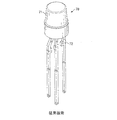
本発明の概念の説明を始める前に、図6及び図7に記載の従来技術の例を見た方がよいであろう。図6は、ランプケース61及び該ランプケースの底部から延びる接点62を有するLED60を示している。上記のように、接点62は、ランプの電気的接点として機能するとともにランプの安定性を確保するための基礎構造(プラットフォーム)を形成するように曲げられている。ただし、もしこれらの接点が正確に均一に曲がっていなければ、ランプケース61はいずれかの方向に傾き、光の強度は望ましくない状態に変化することになる。同様に、図7に示すランプ70は長い脚状接点を有する。脚状接点は回路基板に通すことができ、いずれかの方向へ曲げることによりその表面に取り付けることもできる。ただし、素子70も、素子60と同じ問題を抱えている。
Before beginning to explain the concept of the present invention, it is better to look at the prior art examples described in FIGS. FIG. 6 shows an
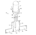
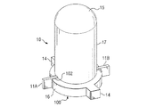
次に図1Aに移ると、図1AはLEDデバイス10を示している。LEDデバイス10はSMT(表面実装)型ランプであってもよい。ケース17の中には、素子19のような、LEDの光を適切な光にするための種々の素子が収容される。例えば、必要であれば、焦点調節素子が収容される。接点構造13は、ケース17内部の素子19に接触させるための上部領域18を有する。接点構造13は接触領域11を更に有し、接触領域11は底面12、並びに側部接触領域11A及び11Bを有する。一実施形態において、接点構造13は、一回のプレス成形によって形成され、接点構造13をケース17の中に嵌め込むと、図1Bに示すように、底面12は、ケース17の底面100に対して平行な位置、又は、ケース17の底面100よりも高い位置にくる。作動したLEDの光は、ケース17の上部15から放出される。
Turning now to FIG. 1A, FIG. 1A shows an
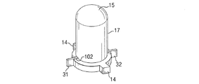
図1Bに示すように、接触部11a及び11bは、ケースに形成されたスロット102を通して延びる。接点構造13をケース17の中に完全に嵌め込んだ後、接点構造13は破線101に沿って切断され、電気的及び機械的に分離される。ケース17は、接触部や関連素子をしっかりと保持する構造を有する。このとき、接触部はケース17の底面上に、又は底面よりも高い平面上にぴったりと位置決めされる。そのため、ケース17の底面100によってLEDを適切な姿勢に維持するための安定性が得られ、ケース17の上部15は所望の平面上に位置決めされる。ケース17の底面積は拡大することもでき、例えば脚部14を長くすることで、表面積は拡大し、安定性を向上させることができる。
As shown in FIG. 1B, the contact portions 11a and 11b extend through a
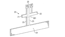
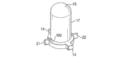
図2Aは、より狭い接触領域23と、直立部(ライザー)23から外側へ向かって垂直に延びる接触部21及び22とを備えた、代替接点構造20を示している。図2Bに示すように、完成後の構造において、張り出し部21及び22の底面は接点を形成する。接点構造20をケース17に嵌め込んだ後、接点構造20は破線201に沿って切断され、23及び24の部分は切り落とされる。製造時には、24の部分により接点構造23の安定性及び剛性が確保され、構造23をケース17の中に適切に挿入することが可能となる。
FIG. 2A shows an
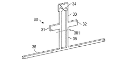
図3Aは、直立部35に対して接触部31及び32が形成された、代替接点構造30を示している。この場合も、接点構造30をケース17に嵌め込んだ後(図3B)、直立部35及び基部36は破線301に沿って切り落される。
FIG. 3A shows an
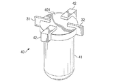
図4は、上で述べたように、ケース41から外側へ向かって放射状に延びる接触部31及び32を備えた代替実施形態40を示している。ケース41は、底面401よりも下(図4では、上)まで延びる2本の脚部42及び43を有し、2本の脚部の底面、即ち両足は、接触部31及び32の底面と同じ平面上に配置され、補助的な支持手段として働く。必要であれば可能な限り多数の脚部を形成し、平面を形成したり、脚部をケース41の一部として一体成形してもよい。
FIG. 4 shows an
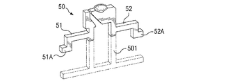
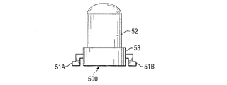
図5Aは代替接点構造50を示している。接点構造50は、ケース52(図5B)の外周よりも更に外側まで延びる足部51a及び52aのような足部を有し、接点構造50をケース52の中に嵌め込んだときに、足部51a及び51bが外側へ向かって放射状に張り出し、安定性を向上させるように構成される。なお、ランプケース52の基部53は、ケース本体より大きくてもよい。接触部51a及び51bの底面をケース52の底面と同じ平面上に配置することで、デバイスを平坦な表面に取り付けたときのデバイスの支持能力及び構造上の安定性が向上する。必要であれば構造50は一回のプレス成形によって形成することができ、余分な材料501は構造50をケース52の中に嵌め込んだ後で切り落とすことができる。
FIG. 5A shows an
本発明及びその利点について詳細に説明したが、特許請求の範囲に規定したような本発明の思想及び範囲から外れることなく、種々の改変、置換、及び変更を行うことが可能であるものと考えられる。また、本発明の範囲を本明細書に記載したプロセス、機械、製造、組成、手段、方法、及びステップ等に関する特定の実施形態に限定する意図はない。当業者であれば、本発明、プロセス、機械、製造、組成、手段、方法、及びステップの開示に基づいて、既存のプロセス、機械、製造、組成、手段、方法、及びステップを本発明に従って使用し、又は将来開発されるであろうそれらを本発明に従って使用し、本明細書に記載した実施形態と実質的に同じ機能を実施したり、実質的に同じ結果を達成したりすることも可能であることは、明らかである。従って、特許請求の範囲には、それらのプロセス、機械、製造、組成、手段、方法、及びステップも含めることを意図している。 Although the present invention and its advantages have been described in detail, it is believed that various modifications, substitutions and changes can be made without departing from the spirit and scope of the present invention as defined in the claims. It is done. Also, there is no intention to limit the scope of the invention to the specific embodiments relating to the processes, machines, manufacture, compositions, means, methods, steps, etc. described herein. One skilled in the art will use existing processes, machinery, manufacture, compositions, means, methods, and steps according to the present invention based on the disclosure of the present invention, processes, machines, manufacture, compositions, means, methods, and steps. Or those that will be developed in the future can be used in accordance with the present invention to perform substantially the same functions and achieve substantially the same results as the embodiments described herein. It is clear that Accordingly, the claims are intended to include those processes, machines, manufacture, compositions of matter, means, methods, and steps.
以下に、本発明の例示的実施形態を列挙する。
1. LEDを製造する方法であって、
予め射出成形された接点の組をLED射出成形されたランプに挿入し、前記接点の組の少なくとも一部が、前記射出成形されたランプの底部から延びるようにするステップと、
前記接点の組のうち、前記射出成形されたランプの底部を超えて延びる部分を全て切り落とすステップと
からなる方法。
2.前記挿入は、前記接点の組の一部が、前記射出成形されたランプの環状の縁を越えて延びるように実施される、1に記載の方法。
3.電気的接点と結合させるためのLED構造を内部に有し、前記電気的接点を受け止めるための領域を備えた基部を有する、予め射出成形されたランプケースと、
単一構造上に形成され、前記ランプ基部を介して前記ランプケースに挿入されるように構成された少なくとも1つの接点の組であって、少なくとも1つの横方向に延びる部分を有し、該横方向に延びる部分は前記ランプ基部から外側へ向かって放射状に延び、該横方向に延びる部分は前記ランプ基部の底面よりも下まで延びないように構成された底面を有する、少なくとも1つの接点の組と
からなるLED。
4.前記ランプケースは円形である、3に記載のLED。
5.前記ランプ基部は、前記ランプケースの主な部分の外周部よりも大きい外周部を持つ部分を有する、4に記載のLED。
6.前記大きい外周部は、前記LEDを基板に取り付けるのに十分な安定性を提供する、5に記載のLED。
7.前記予め射出成形されたランプケースの底部に、前記LEDを基板に取り付けたときの安定性を提供するための、少なくとも1つの張り出した脚部が構成される、3に記載のLED。
8.前記張り出した脚部の底面は、前記横方向に延びる部分の底面と同一平面上に配置される、7に記載のLED。
9. 基板に取り付けるための基部を備えたランプに電力を供給する際に使用する構造であって、
前記ランプ内部の電力を必要とする素子に結合させるための接触部と、前記内部接触部が適切な内部結合関係にあるときに前記ランプから外側へ向かって放射状に延びる接触部とを有する、形成済み電気接点リードの組を有する、構造。
10.前記内部接触部が適切な内部結合関係にあるときに、前記外側へ向かって延びる接触部の底面が前記ランプの底面と実質的に同一平面上になるようにして切り落とすべき部分であって、前記外部接触部に隣接する部分を更に含む、9に記載の構造。
11.前記ランプはLEDであり、前記電力を必要とする内部素子は前記LEDの素子である、10に記載の構造。
12.前記ランプの底面は、前記ランプの底面を基板に取り付けたときに前記ランプの安定性を維持できるくらい広い面積を有する、11に記載の構造。
13.前記ランプの底面は、前記面積を増加させる少なくとも1つのパッドを更に含む、12に記載の構造。
14.前記少なくとも1つのパッドは、前記外側へ向かって延びる接触部の底面と協働し、前記安定性を増加させる、12に記載の構造。
15.前記ランプの底面は、前記LEDが配置されたときに、前記ランプの上部よりも広い断面積を有する、12に記載の構造。
16.前記構造は、前記ランプの長手方向に対して平行に延びる少なくとも一対の支持要素を有し、前記外側へ向かって延びる部分は、前記平行に延びる部分の幅の部分である、10に記載の構造。
17.前記構造は、前記ランプの長手方向に対して平行に延びる少なくとも一対の支持要素を有し、前記外側へ向かって延びる部分は、前記平行に延びる部分から外側へ向かって延びる部分である、10に記載の構造。
18.光を逃がすことが可能な上部を有する円筒状部分と、
基板に対して取り付けるための基部であって、底面を有し、該底面は、該底部を平坦な表面に接触させたときに前記上部を安定した状態に維持することができるくらい広い断面積を有する、基部と、
前記ランプケース内の光生成素子に結合させるための近端を有するとともに、外部ソースから電力を受けとるために、前記基部から外側へ向かって放射状に延びる外側張り出し部を有する接点構造を受け入れる手段と、
前記外側張り出し部を受け止めて支持する位置に設けられた少なくとも2つの領域であって、前記外側張り出し部の底端面が前記基部底面よりも低くならないようにするための、少なくとも2つの領域と
からなるランプケース。
19.前記外側張り出し部の底端面は、前記基部底面と協働し、前記基部が前記平坦な表面に接触しているときに前記ランプ上部の安定性を向上させる、18に記載のランプケース。
20.前記受け入れる手段は、前記ランプ基部の環状の縁部において対向する縁部に設けられた少なくとも一対のスリットからなる、19に記載のランプケース。
The following lists exemplary embodiments of the present invention.
1. A method of manufacturing an LED comprising:
Inserting a pre-injected set of contacts into an LED injection molded lamp so that at least a portion of the set of contacts extends from the bottom of the injection molded lamp;
Cutting off all portions of the set of contacts extending beyond the bottom of the injection molded lamp.
2. The method of claim 1, wherein the insertion is performed such that a portion of the contact set extends beyond an annular edge of the injection molded lamp.
3. A pre-injected lamp case having an LED structure for coupling with an electrical contact therein and having a base with a region for receiving the electrical contact;
A set of at least one contact formed on a single structure and configured to be inserted into the lamp case through the lamp base, the set having at least one laterally extending portion, A directionally extending portion extends radially outward from the lamp base, and the laterally extending portion has a bottom surface configured to not extend below the bottom surface of the lamp base. LED consisting of and.
4). 4. The LED according to 3, wherein the lamp case is circular.
5. 5. The LED according to 4, wherein the lamp base has a portion having an outer peripheral portion larger than an outer peripheral portion of a main portion of the lamp case.
6). 6. The LED of 5, wherein the large outer perimeter provides sufficient stability to attach the LED to a substrate.
7). 4. The LED according to 3, wherein at least one protruding leg is provided on the bottom of the pre-injected lamp case to provide stability when the LED is attached to a substrate.
8). 8. The LED according to 7, wherein a bottom surface of the protruding leg is disposed on the same plane as a bottom surface of the laterally extending portion.
9. A structure used to supply power to a lamp with a base for mounting on a substrate,
Forming a contact portion for coupling to an element that requires electric power inside the lamp, and a contact portion extending radially outward from the lamp when the inner contact portion is in an appropriate inner coupling relationship A structure having a set of finished electrical contact leads.
10. A portion to be cut off so that a bottom surface of the contact portion extending outwardly is substantially flush with a bottom surface of the lamp when the internal contact portion has an appropriate internal coupling relationship; 10. The structure according to 9, further including a portion adjacent to the external contact portion.
11. 11. The structure according to 10, wherein the lamp is an LED, and the internal element that requires power is an element of the LED.
12 12. The structure according to 11, wherein the bottom surface of the lamp has an area large enough to maintain the stability of the lamp when the bottom surface of the lamp is attached to a substrate.
13. 13. The structure of
14 13. The structure of
15. 13. The structure according to 12, wherein the bottom surface of the lamp has a wider cross-sectional area than the top of the lamp when the LED is disposed.
16. 11. The structure according to 10, wherein the structure has at least a pair of support elements extending in parallel to a longitudinal direction of the lamp, and the outwardly extending portion is a width portion of the parallel extending portion. .
17. The structure has at least a pair of support elements extending parallel to the longitudinal direction of the lamp, and the outwardly extending portion is a portion extending outwardly from the parallel extending portion. Description structure.
18. A cylindrical part having an upper part capable of escaping light;
A base for mounting to a substrate having a bottom surface, the bottom surface having a cross-sectional area large enough to keep the top stable when the bottom is in contact with a flat surface. Having a base;
Means for receiving a contact structure having a proximal end for coupling to a light generating element in the lamp case and having an outer overhang extending radially outward from the base for receiving power from an external source;
And at least two regions provided at positions for receiving and supporting the outer overhanging portion, the bottom end surface of the outer overhanging portion not being lower than the bottom surface of the base portion. Lamp case.
19. 19. The lamp case according to 18, wherein a bottom end surface of the outer overhanging portion cooperates with the base bottom surface to improve stability of the lamp upper portion when the base is in contact with the flat surface.
20. 20. The lamp case according to 19, wherein the receiving means comprises at least a pair of slits provided at opposite edges of the annular edge of the lamp base.
13
11A,11B
12 底面
13 接点構造
14 脚部
15 ケース上部
16 基部
17 ケース
18 上部領域
19 素子
102 スロット
13
11A, 11B
12
Claims (11)
予め射出成形された接点の組をLED射出成形されたランプに挿入し、前記接点の組の少なくとも一部が、前記射出成形されたランプの底部から延びるようにするステップと、
前記接点の組のうち、前記射出成形されたランプの底部を超えて延びる部分を全て切り落とすステップと
からなる方法。 A method of manufacturing an LED comprising:
Inserting a pre-injected set of contacts into an LED injection molded lamp so that at least a portion of the set of contacts extends from the bottom of the injection molded lamp;
Cutting off all portions of the set of contacts extending beyond the bottom of the injection molded lamp.
単一構造上に形成され、前記ランプ基部を介して前記ランプケースに挿入されるように構成された少なくとも1つの接点の組(13)であって、少なくとも1つの横方向に延びる部分(11A、11B)を有し、該横方向に延びる部分は前記ランプ基部から外側へ向かって放射状に延び、該横方向に延びる部分は前記ランプ基部の底面よりも下まで延びないように構成された底面(12)を有する、少なくとも1つの接点の組と
からなるLED。 A pre-injected lamp case (17) having an LED structure (19) for coupling with an electrical contact therein and a base (16) with a region (102) for receiving the electrical contact. )When,
A set of at least one contact (13) formed on a single structure and configured to be inserted into the lamp case via the lamp base, wherein the at least one laterally extending portion (11A, 11B), the laterally extending portion extends radially outward from the lamp base, and the laterally extending portion does not extend below the bottom surface of the lamp base. 12) having at least one contact set.
前記ランプ内部の電力を必要とする素子(19)に結合させるための接触部(18)と、前記内部接触部が適切な内部結合関係にあるときに前記ランプから外側へ向かって放射状に延びる接触部(11A,11B)とを有する、形成済み電気接点リードの組(13)を有する、構造。 A structure used to supply power to a lamp with a base for mounting on a substrate,
A contact (18) for coupling to an element (19) requiring electrical power inside the lamp and a contact extending radially outward from the lamp when the internal contact is in an appropriate internal coupling relationship; A structure having a set (13) of pre-formed electrical contact leads having a portion (11A, 11B).
基板に対して取り付けるための基部であって、底面を有し、該底面は、該底部を平坦な表面に接触させたときに前記上部を安定した状態に維持することができるくらい広い断面積を有する、基部(16)と、
前記ランプケース内の光生成素子に結合させるための近端(18)を有するとともに、外部ソースから電力を受けとるために、前記基部から外側へ向かって放射状に延びる外側張り出し部(11A,11B)を有する接点構造(13)を受け入れる手段と、
前記外側張り出し部を受け止めて支持する位置に設けられた少なくとも2つの領域であって、前記外側張り出し部の底端面が前記基部底面よりも低くならないようにするための、少なくとも2つの領域(102)と
からなるランプケース。
A cylindrical portion (17) having an upper portion (15) through which light can escape;
A base for mounting to a substrate having a bottom surface, the bottom surface having a cross-sectional area large enough to keep the top stable when the bottom is in contact with a flat surface. Having a base (16);
In addition to having a proximal end (18) for coupling to a light generating element in the lamp case, outer projecting portions (11A, 11B) that extend radially outward from the base to receive power from an external source. Means for receiving a contact structure (13) comprising:
At least two regions (102) provided at positions for receiving and supporting the outer overhanging portion so that the bottom end surface of the outer overhanging portion does not become lower than the bottom surface of the base portion. A lamp case consisting of and.
Applications Claiming Priority (1)
| Application Number | Priority Date | Filing Date | Title |
|---|---|---|---|
| US11/052,385 US7326062B2 (en) | 2005-02-07 | 2005-02-07 | System and method for increasing the surface mounting stability of a lamp |
Publications (2)
| Publication Number | Publication Date |
|---|---|
| JP2006222425A true JP2006222425A (en) | 2006-08-24 |
| JP2006222425A5 JP2006222425A5 (en) | 2009-03-26 |
Family
ID=36779072
Family Applications (1)
| Application Number | Title | Priority Date | Filing Date |
|---|---|---|---|
| JP2006028189A Pending JP2006222425A (en) | 2005-02-07 | 2006-02-06 | System and method for improving lamp surface mount stability |
Country Status (2)
| Country | Link |
|---|---|
| US (2) | US7326062B2 (en) |
| JP (1) | JP2006222425A (en) |
Families Citing this family (1)
| Publication number | Priority date | Publication date | Assignee | Title |
|---|---|---|---|---|
| CN101459212B (en) * | 2007-12-11 | 2011-06-22 | 富士迈半导体精密工业(上海)有限公司 | Solid illuminating element |
Citations (3)
| Publication number | Priority date | Publication date | Assignee | Title |
|---|---|---|---|---|
| JPS5761859U (en) * | 1980-09-30 | 1982-04-13 | ||
| JPH0690028A (en) * | 1992-09-08 | 1994-03-29 | Stanley Electric Co Ltd | Method for manufacturing surface mount type LED |
| JPH06204568A (en) * | 1992-12-30 | 1994-07-22 | Stanley Electric Co Ltd | Lead frame terminal structure |
Family Cites Families (10)
| Publication number | Priority date | Publication date | Assignee | Title |
|---|---|---|---|---|
| JPH03148896A (en) * | 1989-11-06 | 1991-06-25 | Furukawa Electric Co Ltd:The | Circuit board for mounting photo-detector and light-emitting device |
| JPH0737272Y2 (en) * | 1993-06-16 | 1995-08-23 | 第一電装部品株式会社 | Attachment mounting structure |
| JP4138586B2 (en) * | 2003-06-13 | 2008-08-27 | スタンレー電気株式会社 | LED lamp for light source and vehicle headlamp using the same |
| US6809261B1 (en) * | 2003-06-23 | 2004-10-26 | Agilent Technologies, Inc. | Physically compact device package |
| JP2005197369A (en) * | 2004-01-05 | 2005-07-21 | Toshiba Corp | Optical semiconductor device |
| US7053414B2 (en) * | 2004-04-12 | 2006-05-30 | Lite-On Technology Corporation | Optical semiconductor component to prevent electric leakage and provide different driving voltages |
| US20050248259A1 (en) * | 2004-05-10 | 2005-11-10 | Roger Chang | Bent lead light emitting diode device having a heat dispersing capability |
| US7456499B2 (en) * | 2004-06-04 | 2008-11-25 | Cree, Inc. | Power light emitting die package with reflecting lens and the method of making the same |
| US7280288B2 (en) * | 2004-06-04 | 2007-10-09 | Cree, Inc. | Composite optical lens with an integrated reflector |
| US7777247B2 (en) * | 2005-01-14 | 2010-08-17 | Cree, Inc. | Semiconductor light emitting device mounting substrates including a conductive lead extending therein |
-
2005
- 2005-02-07 US US11/052,385 patent/US7326062B2/en not_active Expired - Lifetime
-
2006
- 2006-02-06 JP JP2006028189A patent/JP2006222425A/en active Pending
-
2007
- 2007-12-04 US US11/950,323 patent/US7648260B2/en not_active Expired - Fee Related
Patent Citations (3)
| Publication number | Priority date | Publication date | Assignee | Title |
|---|---|---|---|---|
| JPS5761859U (en) * | 1980-09-30 | 1982-04-13 | ||
| JPH0690028A (en) * | 1992-09-08 | 1994-03-29 | Stanley Electric Co Ltd | Method for manufacturing surface mount type LED |
| JPH06204568A (en) * | 1992-12-30 | 1994-07-22 | Stanley Electric Co Ltd | Lead frame terminal structure |
Also Published As
| Publication number | Publication date |
|---|---|
| US7648260B2 (en) | 2010-01-19 |
| US7326062B2 (en) | 2008-02-05 |
| US20060175615A1 (en) | 2006-08-10 |
| US20080085622A1 (en) | 2008-04-10 |
Similar Documents
| Publication | Publication Date | Title |
|---|---|---|
| US20080128255A1 (en) | Arrangement for surface mounting an electrical component by soldering, and electrical component for such an arrangement | |
| JP2006054105A (en) | Connector of floating structure | |
| JP4811530B1 (en) | Terminal and connector using the same | |
| JP4943930B2 (en) | Mounting structure of 3D circuit parts | |
| US7172433B2 (en) | Electrical connector having elastic terminals with contacts located at the same level | |
| JP2006222425A (en) | System and method for improving lamp surface mount stability | |
| KR100888240B1 (en) | Lens drive motor | |
| JP2003242857A (en) | Moving contact body for push-button switch and switch device using it | |
| JP2022128778A (en) | Connector and assembly | |
| CN102651508B (en) | RF connector | |
| KR101041236B1 (en) | Touch sensor and manufacturing method | |
| JP4326861B2 (en) | Duct rail inverter case mounting structure | |
| KR20180036874A (en) | Pcb connector and method for manufacturing thereof | |
| KR101431907B1 (en) | Terminal Socket for Power Supply | |
| US20040046507A1 (en) | Lamp base comprising an eletronic component and a method for producing a lamp base | |
| JPH114050A (en) | Circuit board | |
| JPS6317186Y2 (en) | ||
| JPH0719113Y2 (en) | Light bulb socket | |
| JP2000113773A (en) | Rotary switch | |
| JP2025080307A (en) | Lighting fixtures | |
| KR200372232Y1 (en) | A ballast case for a 2D lamp | |
| JPH069372Y2 (en) | Fluorescent lamp holding structure for lighting equipment | |
| JPH058768Y2 (en) | ||
| US20070275574A1 (en) | Chip Assembly Structure With Cover | |
| JPH056787A (en) | Plcc socket and mounting method on its base |
Legal Events
| Date | Code | Title | Description |
|---|---|---|---|
| A521 | Request for written amendment filed |
Free format text: JAPANESE INTERMEDIATE CODE: A523 Effective date: 20090205 |
|
| A621 | Written request for application examination |
Free format text: JAPANESE INTERMEDIATE CODE: A621 Effective date: 20090205 |
|
| A711 | Notification of change in applicant |
Free format text: JAPANESE INTERMEDIATE CODE: A711 Effective date: 20090414 |
|
| A131 | Notification of reasons for refusal |
Free format text: JAPANESE INTERMEDIATE CODE: A131 Effective date: 20110913 |
|
| A521 | Request for written amendment filed |
Free format text: JAPANESE INTERMEDIATE CODE: A523 Effective date: 20111213 |
|
| A131 | Notification of reasons for refusal |
Free format text: JAPANESE INTERMEDIATE CODE: A131 Effective date: 20120612 |
|
| A02 | Decision of refusal |
Free format text: JAPANESE INTERMEDIATE CODE: A02 Effective date: 20121106 |