JP2006229155A - Wiring circuit substrate - Google Patents
Wiring circuit substrate Download PDFInfo
- Publication number
- JP2006229155A JP2006229155A JP2005044454A JP2005044454A JP2006229155A JP 2006229155 A JP2006229155 A JP 2006229155A JP 2005044454 A JP2005044454 A JP 2005044454A JP 2005044454 A JP2005044454 A JP 2005044454A JP 2006229155 A JP2006229155 A JP 2006229155A
- Authority
- JP
- Japan
- Prior art keywords
- insulating layer
- terminal
- external connection
- base insulating
- connection terminal
- Prior art date
- Legal status (The legal status is an assumption and is not a legal conclusion. Google has not performed a legal analysis and makes no representation as to the accuracy of the status listed.)
- Granted
Links
Images


Landscapes
- Non-Metallic Protective Coatings For Printed Circuits (AREA)
- Printing Elements For Providing Electric Connections Between Printed Circuits (AREA)
- Structure Of Printed Boards (AREA)
- Adjustment Of The Magnetic Head Position Track Following On Tapes (AREA)
Abstract
【課題】 端子部のベース絶縁層からの剥離を確実に防止しつつ、端子部と外部接続部材との確実な接続を確保することができ、端子部と外部接続部材との接続信頼性を向上させることのできる、配線回路基板を提供すること。
【解決手段】 ベース絶縁層3に、各外部側接続端子9から連続する各配線10の後端13に対応して、端子凹部11を形成し、各端子凹部11内に各配線10の後端13を配置するとともに、各端子凹部11内において、各外部側接続端子9のベース絶縁層3からの剥離を防止するために、各後端13を被覆するように、剥離防止部16を設ける。これによって、各剥離防止部16の上面を、各層の積層方向において、各外部側接続端子9の上面と等しく配置するか、または、各外部側接続端子9の上面よりもベース絶縁層3側に配置して、リード・ライト基板31の各剥離防止部16に対する干渉を回避する。
【選択図】 図4PROBLEM TO BE SOLVED: To ensure reliable connection between a terminal part and an external connection member while reliably preventing peeling of the terminal part from a base insulating layer, and to improve connection reliability between the terminal part and the external connection member Provided is a printed circuit board that can be made to operate.
A terminal recess 11 is formed in a base insulating layer 3 corresponding to a rear end 13 of each wiring 10 continuous from each external connection terminal 9, and a rear end of each wiring 10 is formed in each terminal recess 11. 13, and in each terminal recess 11, a peeling preventing portion 16 is provided so as to cover each rear end 13 in order to prevent peeling of each external connection terminal 9 from the base insulating layer 3. Accordingly, the upper surface of each peeling prevention portion 16 is arranged equal to the upper surface of each external connection terminal 9 in the stacking direction of each layer, or closer to the base insulating layer 3 than the upper surface of each external connection terminal 9. Arrangement is made to avoid interference of the read / write board 31 with respect to each peeling prevention portion 16.
[Selection] Figure 4
Description
本発明は、配線回路基板、詳しくは、回路付サスペンション基板などの配線回路基板に関する。 The present invention relates to a wired circuit board, and more particularly to a wired circuit board such as a suspension board with circuit.
配線回路基板は、通常、カバー絶縁層と、そのカバー絶縁層の上に形成される導体パターンと、その導体パターンを被覆するようにカバー絶縁層の上に形成されるカバー絶縁層とを備えている。
このような配線回路基板には、電子部品を実装したり、他の配線回路基板と接続したり、あるいは、コネクタに差し込むための端子部が、例えば、配線回路基板の端部において、導体パターンの一部として設けられている。このような端子部は、例えば、導体パターンの端部においてランドとして形成され、カバー絶縁層は、そのランドが露出するように、導体パターンの途中までを被覆するように形成されている。
A wired circuit board usually includes a cover insulating layer, a conductor pattern formed on the cover insulating layer, and a cover insulating layer formed on the cover insulating layer so as to cover the conductor pattern. Yes.
In such a printed circuit board, a terminal part for mounting an electronic component, connecting to another printed circuit board, or being inserted into a connector is, for example, a conductor pattern at an end of the printed circuit board. It is provided as a part. Such a terminal portion is formed as a land at the end portion of the conductor pattern, for example, and the cover insulating layer is formed so as to cover part of the conductor pattern so that the land is exposed.
また、端子部の接続信頼性を向上させるためには、端子部がベース絶縁層から剥離することを防止する必要がある。そのため、例えば、配線回路基板の端部において、ベースフィルムの上に、本体側カバーフィルムから露出する端子部の遊端部を被覆する先端側カバーフィルムを設けることが知られている(例えば、特許文献1参照。)。
しかし、上記のように、先端側カバーフィルムを設けると、その先端側カバーフィルムは、端子部の遊端部に被覆されるため、その端子部に接続される電子部品、他の配線回路基板あるはコネクタの接続部分が、先端側カバーフィルムと干渉して、却って端子部の接続信頼性を損ねるおそれがある。
本発明の目的は、端子部のベース絶縁層からの剥離を確実に防止しつつ、端子部と外部接続部材との確実な接続を確保することができ、端子部と外部接続部材との接続信頼性を向上させることのできる、配線回路基板を提供することにある。
However, as described above, when the front end side cover film is provided, the front end side cover film is covered with the free end portion of the terminal portion, so there are electronic components connected to the terminal portion, and other wired circuit boards. In this case, there is a possibility that the connection portion of the connector interferes with the front end side cover film, and on the contrary, the connection reliability of the terminal portion is impaired.
The object of the present invention is to ensure the reliable connection between the terminal part and the external connection member while reliably preventing the terminal part from peeling off from the base insulating layer, and to ensure the connection between the terminal part and the external connection member. An object of the present invention is to provide a printed circuit board capable of improving the performance.
上記の目的を達成するため、本発明の配線回路基板は、ベース絶縁層と、前記ベース絶縁層の上に形成され、外部接続部材と接続される端子部を含む導体パターンと、前記端子部の前記ベース絶縁層からの剥離を防止するために、前記導体パターンを被覆するように、前記ベース絶縁層の上に形成された剥離防止カバー絶縁層とを備える配線回路基板において、前記剥離防止カバー絶縁層は、その表面が、前記ベース絶縁層と前記導体パターンとの積層方向において、前記端子部の表面と等しく配置されるか、または、前記端子部の表面に対して前記ベース絶縁層側に配置されていることを特徴としている。 In order to achieve the above object, a wired circuit board according to the present invention includes a base insulating layer, a conductor pattern formed on the base insulating layer and including a terminal portion connected to an external connection member, and the terminal portion. In a printed circuit board comprising a peeling prevention cover insulating layer formed on the insulating base layer so as to cover the conductor pattern in order to prevent peeling from the insulating base layer, the peeling prevention cover insulation The surface of the layer is disposed equal to the surface of the terminal portion in the stacking direction of the base insulating layer and the conductor pattern, or is disposed on the base insulating layer side with respect to the surface of the terminal portion. It is characterized by being.
また、本発明の配線回路基板は、前記剥離防止カバー絶縁層が、前記端子部に接続される前記外部接続部材との対向位置に配置されている場合に、好適である。
また、本発明の配線回路基板では、前記ベース絶縁層には、前記ベース絶縁層と前記導体パターンとの積層方向において、一方が前記外部接続部材に近接し、他方が前記外部接続部材から離間する段差が形成されており、前記剥離防止カバー絶縁層は、前記段差に対して、前記外部接続部材から離間する他方側に配置されていることが好適である。
The wired circuit board according to the present invention is suitable when the peeling prevention cover insulating layer is disposed at a position facing the external connection member connected to the terminal portion.
In the wired circuit board of the present invention, one of the base insulating layer is close to the external connection member and the other is separated from the external connection member in the stacking direction of the base insulating layer and the conductor pattern. It is preferable that a step is formed, and the peeling prevention cover insulating layer is disposed on the other side away from the external connection member with respect to the step.
本発明の配線回路基板によれば、剥離防止カバー絶縁層の表面が、ベース絶縁層と導体パターンとの積層方向において、端子部の表面と等しく配置されるか、または、端子部の表面に対してベース絶縁層側に配置されている。そのため、外部接続部材を、剥離防止カバー絶縁層と対向するようにして端子部と接続しても、外部接続部材の剥離防止カバー絶縁層に対する干渉を回避しつつ、外部接続部材を端子部に接続することができる。その結果、端子部のベース絶縁層からの剥離を確実に防止しつつ、端子部と外部接続部材との確実な接続を確保することができ、端子部と外部接続部材との接続信頼性を向上させることができる。 According to the wired circuit board of the present invention, the surface of the peeling prevention cover insulating layer is arranged to be equal to the surface of the terminal portion in the stacking direction of the base insulating layer and the conductor pattern or to the surface of the terminal portion. Are disposed on the base insulating layer side. Therefore, even if the external connection member is connected to the terminal part so as to face the peeling prevention cover insulating layer, the external connection member is connected to the terminal part while avoiding interference with the peeling prevention cover insulating layer of the external connection member. can do. As a result, it is possible to ensure the reliable connection between the terminal portion and the external connection member while reliably preventing the terminal portion from being peeled off from the base insulating layer, and to improve the connection reliability between the terminal portion and the external connection member. Can be made.
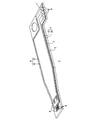
図1は、本発明の配線回路基板の一実施形態である回路付サスペンション基板を示す斜視図、図2は、図1に示す回路付サスペンション基板の端子配置部の要部平面図であり、図3は、図2におけるA−A線断面図、図4は、図2におけるB−B線断面図である。
図1において、この回路付サスペンション基板1は、ハードディスクドライブの磁気ヘッド(図示せず)を実装して、その磁気ヘッドを、磁気ヘッドと磁気ディスクとが相対的に走行する時の空気流に抗して、磁気ディスクとの間に微小な間隔を保持しながら支持するものであり、磁気ヘッドと、リード・ライト基板31(図4参照)とを接続するための導体パターン4が一体的に形成されている。
FIG. 1 is a perspective view showing a suspension board with circuit as an embodiment of the wired circuit board of the present invention, and FIG. 2 is a plan view of a principal part of a terminal arrangement portion of the suspension board with circuit shown in FIG. 3 is a sectional view taken along line AA in FIG. 2, and FIG. 4 is a sectional view taken along line BB in FIG.
In FIG. 1, this suspension board with
この回路付サスペンション基板1は、図4に示すように、支持基板2と、支持基板2の上に形成されたベース絶縁層3と、ベース絶縁層3の上に形成された導体パターン4と、導体パターン4を被覆するように、ベース絶縁層3の上に形成されたカバー絶縁層5とを備えている。なお、図1では、カバー絶縁層5が省略されている。
支持基板2は、図1において、長手方向に延びる薄板からなり、その先端部には、磁気ヘッドを実装するためのジンバル6が形成されており、また、その後端部には、後述する各外部側接続端子9を、支持基板2の長手方向に沿って配置するための端子配置部7が、幅方向(支持基板2の長手方向に直交する方向)の一方側に、平面視略矩形状に膨出するように形成されている。なお、支持基板2の厚みは、例えば、10〜100μm、好ましくは、18〜30μmであり、その幅は、例えば、50〜500mm、好ましくは、125〜300mmである。
As shown in FIG. 4, the suspension board with
The
ベース絶縁層3は、支持基板2における導体パターン4が形成される部分を含む所定のパターンとして形成されている。ベース絶縁層3の厚みは、例えば、8〜25μm、好ましくは、10〜15μmである。
ベース絶縁層3には、端子配置部7において、図2〜図4に示すように、後述する各外部側接続端子9から連続する各配線10の後端13に対応して、端子凹部11が複数(4つ)形成されている。各端子凹部11は、後述する各外部側接続端子9にリード・ライト基板31の各端子32が接続されたときに、リード・ライト基板31との対向位置に形成されている。各端子凹部11は、後述する各配線10の端子配置部7における長手方向(回路付サスペンション基板1の幅方向、以下、配線10の長手方向とする。)において、後述する外部側接続端子9の後端から、後述する剥離防止部16が形成される部分までを含み、かつ、配線10の幅方向(配線10の長手方向と直交する方向)において、後述する剥離防止部16が形成される部分を含むように、平面視略矩形状に形成されている。
The
As shown in FIGS. 2 to 4, in the
各端子凹部11の厚みは、各端子凹部11以外のベース絶縁層3の厚みを100%としたときの、例えば、15〜90%、好ましくは、20〜70%に設定されている。
また、各端子凹部11における周端縁12の段差D(各端子凹部11の表面と、各端子凹部11以外のベース絶縁層3の表面との差)は、例えば、2〜23.5μm、好ましくは、4〜23μmに設定されている。
The thickness of each terminal recess 11 is set to, for example, 15 to 90%, preferably 20 to 70% when the thickness of the
The step D of the
これによって、後述する各外部側接続端子9にリード・ライト基板31の各端子32が接続されたときに、各端子凹部11における周端縁12に対して、各端子凹部11内の表面が、リード・ライト基板31と離間し、各端子凹部11の外側の表面が、リード・ライト基板31と近接するように配置される。
導体パターン4は、図1に示すように、磁気ヘッド側接続端子8と、端子部としての外部側接続端子9と、磁気ヘッド側接続端子8および外部側接続端子9を接続する複数の配線10とを一体的に備えている。複数の配線10は、支持基板2の長手方向に沿って延び、その幅方向において、互いに間隔を隔てて並列配置されている。導体パターン4の厚みは、例えば、5〜20μm、好ましくは、7〜15μmである。また、各配線10の幅は、例えば、5〜500μm、好ましくは、10〜200μmであり、各配線10間の間隔は、例えば、5〜500μm、好ましくは、10〜200μmである。
Thereby, when each
As shown in FIG. 1, the
磁気ヘッド側接続端子8は、支持基板2の先端部に配置され、各配線10に対応して、それぞれ設けられている。各磁気ヘッド側接続端子8は、各配線10の先端部から連続して、幅広のランドとして一体的に形成されており、支持基板2の幅方向に沿って、互いに間隔を隔てて配置されている。この磁気ヘッド側接続端子8には、磁気ヘッド(図示せず)が実装される。
The magnetic head side connection terminals 8 are disposed at the tip of the
外部側接続端子9は、支持基板2の後端部であって、端子配置部7に配置され、各配線10に対応して、それぞれ設けられている。各外部側接続端子9には、外部接続部材としてのリード・ライト基板31の各端子32が接続される。
各外部側接続端子9は、図2に示すように、各配線10の後端部において、各配線10の後端13が残存するように、各配線10の長手方向途中に設けられている。各外部側接続端子9は、配線10の幅方向に膨出する平面視略矩形状のランドとして形成されている。なお、各外部側接続端子9の長さ(配線10の長手方向の長さ)は、例えば、20〜1500μm、好ましくは、50〜1000μmに設定され、その幅(配線10の幅方向における長さ)は、例えば、100〜1100μm、好ましくは、140〜540μmに設定されている。また、各外部側接続端子部9間の間隔は、例えば、20〜1000μm、好ましくは、50〜500μmに設定されている。
The
As shown in FIG. 2, each
また、各外部側接続端子9は、図4に示すように、配線10の長手方向において、各端子凹部11の周端縁12に対して、端子凹部11の外側(先端側)に配置されている。一方、各外部側接続端子9から連続する各配線10の後端13は、各端子凹部11の周端縁12に対して、端子凹部11内に配置されている。これによって、各外部側接続端子9と各配線10の後端13との間には、各端子凹部11の周端縁12の段差に起因して、段差部14が形成されている。
Further, as shown in FIG. 4, each external-
カバー絶縁層4は、後端13を除く各配線10を被覆する配線被覆部15と、各配線10の後端13を被覆する剥離防止カバー絶縁層としての剥離防止部16とを備えている。なお、カバー絶縁層4(配線被覆部15および剥離防止部16を含む。)の厚みは、例えば、2〜15μm、好ましくは、4〜10μmである。
配線被覆部15は、磁気ヘッド側接続端子8および外部側接続端子9を除く各配線10(後端13を除く。)を被覆するように、ベース絶縁層3の上に、所定のパターンで形成されている。
The insulating
The
配線被覆部15は、端子配置部7においては、図2に示すように、各外部側接続端子9よりも配線10の長手方向先端側(回路付サスペンション基板1の幅方向内側)まで形成されており、それより、配線10の長手方向後端側(回路付サスペンション基板1の幅方向外側)に配置されている各外部側接続端子9および各配線10の後端13が、配線被覆部15から露出されている。
As shown in FIG. 2, the
剥離防止部16は、各外部側接続端子9にリード・ライト基板31の端子32が接続されたときに、リード・ライト基板31との対向位置であって、各配線10の後端13に対応して複数設けられている。
各剥離防止部16は、図3および図4に示すように、各端子凹部11内において、各外部側接続端子9のベース絶縁層3からの剥離を防止するために、各配線10の後端13を被覆するように、配線10の幅方向に延びるように設けられている。より具体的には、各剥離防止部16は、配線10の幅方向中央部先端側が各後端13に対向し、配線10の幅方向中央部後端側および配線10の幅方向両端部が各端子凹部11に対向する平面視略矩形細長形状に形成されている。
The
As shown in FIGS. 3 and 4, each peeling
なお、各剥離防止部16は、配線10の幅方向両端部が各端子凹部11の周端縁12に接触するように配置され、配線10の長手方向後端部が、各端子凹部11の周端縁12と配線10の長手方向において間隔を隔てて対向配置されている。
そして、各剥離防止部16は、このように、各端子凹部11内に配置されていることから、各剥離防止部16の上面が、各層(支持基板2、ベース絶縁層3、導体パターン4およびカバー絶縁層5)の積層方向において、各外部側接続端子9の上面と等しく配置されるか、または、各外部側接続端子9の上面よりもベース絶縁層3側に配置されている。好ましくは、各剥離防止部16の上面は、各外部側接続端子9の上面よりも、例えば、1〜7μm、好ましくは、2〜5μmベース絶縁層3側に配置されている。
In addition, each peeling
And since each peeling
また、この回路付サスペンション基板1では、各磁気ヘッド側接続端子部8および各外部側接続端子部9に、これらの表面を被覆保護するためのめっき層23が形成されている。
めっき層23は、金めっき層やニッケルめっき層からなり、めっき層23の厚みは、例えば、ニッケルめっき層である場合には、例えば、0.5〜5μm、金めっき層である場合には、例えば、0.05〜3μmである。
In the suspension board with
The
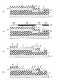
次に、この回路付サスペンション基板1の製造方法を、図5〜図8を参照しつつ説明する。なお、図5〜図8では、図4に対応する断面として示している。
この方法では、まず、図5(a)に示すように、支持基板2を用意する。支持基板2としては、金属箔または金属薄板が用いられ、その金属としては、例えば、ステンレス、42アロイ、アルミニウム、銅−ベリリウム、りん青銅などが用いられる。剛性、耐食性および加工性の観点から、好ましくは、ステンレス箔が用いられる。
Next, a method for manufacturing the suspension board with
In this method, first, a
次いで、この方法では、図5(b)に示すように、支持基板2の上に、ベース絶縁層3を、所定のパターンで形成する。
ベース絶縁層3を形成するための絶縁材料としては、特に制限されないが、例えば、ポリイミド樹脂、ポリアミドイミド樹脂、アクリル樹脂、ポリエーテルニトリル樹脂、ポリエーテルスルホン樹脂、ポリエチレンテレフタレート樹脂、ポリエチレンナフタレート樹脂、ポリ塩化ビニル樹脂などの合成樹脂が用いられる。これらのうち、好ましくは、耐熱性および耐薬品性の観点から、ポリイミド樹脂が用いられる。また、好ましくは、パターンの微細加工の容易性の観点から、感光性の合成樹脂が用いられ、さらに好ましくは、感光性ポリイミド樹脂が用いられる。
Next, in this method, as shown in FIG. 5B, the
The insulating material for forming the
そして、例えば、感光性ポリイミド樹脂を用いて、支持基板2の上に、ベース絶縁層3を所定のパターンで形成する場合には、まず、図6(a)に示すように、感光性ポリイミド樹脂の前駆体(感光性ポリアミック酸樹脂)のワニスを、支持基板2の全面に塗工した後、例えば、60〜150℃、好ましくは、80〜120℃で加熱して、感光性ポリイミド樹脂の前駆体の皮膜17を形成する。
For example, when forming the
次に、図6(b)に示すように、その皮膜17を、フォトマスク18を介して露光する。フォトマスク18は、遮光部分18a、光半透過部分18bおよび光全透過部分18cを所定のパターンで備えている。なお、光半透過部分18bにおいては、光透過率が1〜99%のうちから適宜選択される光透過率で、光が透過される。
そして、支持基板2におけるベース絶縁層3を形成しない周縁部には、遮光部分18aが対向し、支持基板2におけるベース絶縁層3の接続凹部11を形成する部分には、光半透過部分18bが対向し、支持基板2における接続凹部11以外のベース絶縁層3を形成する部分には、光全透過部分18cが対向するように、フォトマスク18を皮膜17に対して対向配置する。
Next, as shown in FIG. 6B, the
The
また、フォトマスク18を介して照射する光(照射線)は、その露光波長が、例えば、300〜450nmであり、その露光積算光量が、例えば、100〜2000mJ/cm2である。
次いで、図6(c)に示すように、露光された皮膜17を、必要により所定温度に加熱した後、現像する。照射された皮膜17の露光部分は、例えば、130℃以上150℃未満で加熱することにより、次の現像において可溶化(ポジ型)し、また、例えば、150℃以上200℃以下で加熱することにより、次の現像において不溶化(ネガ型)する。
Moreover, the light (irradiation line) irradiated through the
Next, as shown in FIG. 6C, the exposed
また、現像には、例えば、アルカリ現像液などの公知の現像液を用いる、浸漬法やスプレー法などの公知の方法が用いられる。なお、この方法においては、ネガ型でパターンを形成することが好ましく、図6においては、ネガ型でパターンを形成している。
この現像により、皮膜17は、フォトマスク18の光全透過部分18cが対向していた部分が残存し、フォトマスク18の遮光部分18aが対向していた周縁部が溶解して、皮膜17は、支持基板2の周縁部が露出される所定のパターンに形成される。また、フォトマスク18の半透過部分18bが対向していた接続凹部11を形成する部分では、皮膜17が、光透過率に対応する割合で残存するように溶解して、接続凹部11が形成される。
For the development, for example, a known method such as an immersion method or a spray method using a known developer such as an alkali developer is used. In this method, it is preferable to form a negative pattern, and in FIG. 6, the negative pattern is formed.
As a result of this development, the
そして、図6(d)に示すように、接続凹部11を含む所定のパターンに形成された皮膜17を、例えば、最終的に250℃以上に加熱することによって、硬化(イミド化)させる。これによって、ポリイミド樹脂からなるベース絶縁層3が、接続凹部11が形成され、支持基板2の周縁部が露出されるような、所定のパターンとして形成される。
なお、感光性の合成樹脂を用いない場合には、例えば、支持基板2の上に、ドライフィルムを、融着または必要により接着剤層を介して貼着した後、プラズマやレーザによるドライエッチングまたはアルカリ水溶液を用いるウエットエッチングなどによって、接続凹部11を形成するとともに、支持基板2の周縁部が露出されるような、所定のパターンとしてベース絶縁層3を形成する。
And as shown in FIG.6 (d), the film |
In the case where a photosensitive synthetic resin is not used, for example, a dry film is adhered on the
次いで、この方法では、図5(c)に示すように、導体パターン4を形成する。導体パターン4を形成するための導体材料としては、特に制限されないが、例えば、銅、ニッケル、金、はんだ、またはこれらの合金などが用いられ、導電性、廉価性および加工性の観点から、好ましくは、銅が用いられる。
また、導体パターン4の形成は、サブトラクティブ法やアディティブ法などの公知のパターンニング法が用いられる。導体パターン4を、ファインピッチで微細に形成するには、好ましくは、アディティブ法が用いられる。
Next, in this method, as shown in FIG. 5C, the
The
アディティブ法では、まず、図7(a)に示すように、ベース絶縁層3から露出する支持基板2の表面と、ベース絶縁層3の全面とに、種膜として、金属薄膜19を形成する。金属薄膜19を形成するための金属材料としては、例えば、クロム、ニッケル、銅およびこれらの合金などが用いられる。また、金属薄膜19の形成は、特に制限されないが、例えば、スパッタリング法などの真空蒸着法が用いられる。金属薄膜19の厚みは、例えば、100〜2000Åである。また、金属薄膜19は、例えば、クロム薄膜と銅薄膜とを順次スパッタリング法により形成するなど、多層で形成することもできる。
In the additive method, first, as shown in FIG. 7A, a metal
次いで、アディティブ法では、図7(b)に示すように、金属薄膜19の表面に、めっきレジスト20を、導体パターン4の反転パターンで形成する。より具体的には、めっきレジスト20は、金属薄膜19の表面に、複数の配線10、各磁気ヘッド側接続端子部8および各外部側接続端子部9に対応する部分の金属薄膜19が露出するように形成される。
Next, in the additive method, as shown in FIG. 7B, a plating resist 20 is formed on the surface of the metal
めっきレジスト20は、例えば、ドライフィルムレジストなどを用いて、公知の方法により、上記した導体パターン4の反転パターンとして形成する。
次いで、アディティブ法では、図7(c)に示すように、めっきレジスト20から露出する金属薄膜19の表面に、導体パターン4を形成する。導体パターン4の形成は、特に制限されないが、例えば、電解めっき、好ましくは、電解銅めっきが用いられる。
The plating resist 20 is formed as a reverse pattern of the above-described
Next, in the additive method, as shown in FIG. 7C, the
その後、図7(d)に示すように、めっきレジスト20を除去する。めっきレジスト20の除去は、例えば、化学エッチング(ウェットエッチング)などの公知のエッチング法を用いるか、または、剥離する。
そして、図7(e)に示すように、導体パターン4から露出する金属薄膜19を除去する。金属薄膜19の除去は、例えば、化学エッチング(ウェットエッチング)する。
Thereafter, as shown in FIG. 7D, the plating resist 20 is removed. For removing the plating resist 20, for example, a known etching method such as chemical etching (wet etching) is used, or peeling is performed.
Then, as shown in FIG. 7E, the metal
これによって、導体パターン4として、図1に示すように、複数の配線10、各磁気ヘッド側接続端子部8および各外部側接続端子部9が一体的に形成される。なお、図1では、図7で示す金属薄膜19が省略されている。
なお、導体パターン4の表面には、その後に、無電解ニッケルめっきにより、ニッケルめっき層(図示せず)を形成して、導体パターン4を保護することが好適である。
As a result, as shown in FIG. 1, a plurality of
It is preferable to protect the
次いで、この方法では、図5(d)に示すように、ベース絶縁層3の上に、導体パターン4のうち、各配線10(各配線10の後端13を除く。)が被覆され、かつ、各磁気ヘッド側接続端子部8、各外部側接続端子部9および各配線10の後端13が露出されるように、カバー絶縁層5を所定のパターンで形成する。
カバー絶縁層5を形成するための絶縁材料としては、ベース絶縁層3と同様の絶縁材料が用いられ、好ましくは、感光性ポリイミド樹脂が用いられる。
Next, in this method, as shown in FIG. 5D, each wiring 10 (excluding the
As an insulating material for forming the insulating
そして、例えば、感光性ポリイミド樹脂を用いて、ベース絶縁層3の上に、カバー絶縁層5を所定のパターンで形成するには、まず、図8(a)に示すように、感光性ポリイミド樹脂の前駆体(感光性ポリアミック酸樹脂)の溶液を、導体パターン4を含むベース絶縁層3および支持基板2の全面に塗工した後、例えば、60〜150℃、好ましくは、80〜120℃で加熱して、感光性ポリイミド樹脂の前駆体の皮膜21を形成する。
For example, in order to form the insulating
次に、図8(b)に示すように、その皮膜21を、フォトマスク22を介して露光する。フォトマスク22は、遮光部分22aおよび光全透過部分22bを所定のパターンで備えている。
そして、皮膜21に対して、カバー絶縁層5の配線被覆部15および剥離防止部16に対応する部分には、光全透過部分22bが対向し、それ以外の各磁気ヘッド側接続端子部8および各外部側接続端子部9に対応する部分を含む部分には、遮光部分22aが対向するように、フォトマスク22を皮膜21に対して対向配置する。次いで、上記した皮膜17の露光と同様に、露光する。
Next, as shown in FIG. 8B, the
Then, a portion corresponding to the
次いで、図8(c)に示すように、露光された皮膜21を、上記した皮膜17の現像と同様に、現像する。なお、図8においては、ネガ型でパターンを形成している。
この現像により、皮膜21は、フォトマスク22の遮光部分22aが対向していた各磁気ヘッド側接続端子部8および各外部側接続端子部9に対応する部分を含む部分が溶解して、支持基板2の周縁部、各磁気ヘッド側接続端子部8および各外部側接続端子部9が露出する所定のパターンに形成される。
Next, as shown in FIG. 8C, the exposed
As a result of this development, the
そして、図8(d)に示すように、所定のパターンに形成された皮膜21を、例えば、最終的に250℃以上に加熱することによって、硬化(イミド化)させる。これによって、ポリイミド樹脂からなるカバー絶縁層5が、各磁気ヘッド側接続端子部8および各外部側接続端子部9が露出され、後端13を除く各配線10を被覆する配線被覆部15と、各配線10の後端13を被覆する剥離防止部16とが形成されるような、所定のパターンとして形成される。
And as shown in FIG.8 (d), the membrane | film |
なお、感光性の合成樹脂を用いない場合には、例えば、ベース絶縁層3の上に、ドライフィルムを、融着または必要により接着剤層を介して貼着した後、プラズマやレーザによるドライエッチングまたはアルカリ水溶液を用いるウエットエッチングなどによって、各磁気ヘッド側接続端子部8および各外部側接続端子部9が露出され、後端13を除く各配線10を被覆する配線被覆部15と、各配線10の後端13を被覆する剥離防止部16とが形成されるような、所定のパターンとしてカバー絶縁層5を形成する。
In the case where a photosensitive synthetic resin is not used, for example, a dry film is adhered on the
その後、この方法では、図5(e)に示すように、各磁気ヘッド側接続端子部8および各外部側接続端子部9に、これらの表面を被覆保護するためのめっき層23を形成する。めっき層23を形成するためのめっき材料は、特に制限されず、例えば、ニッケルや金などが用いられる。また、めっき層23の形成は、例えば、電解めっきまたは無電解めっきが用いられる。また、めっき層23は、ニッケルおよび金を順次めっきすることにより、多層として形成することもできる。
Thereafter, in this method, as shown in FIG. 5E, a
そして、支持基板2を、化学エッチングなど公知の方法によって、ジンバル6の切り抜きとともに、外形加工し、洗浄および乾燥することにより、図1に示すような回路付サスペンション基板1を得る。なお、支持基板2の外形加工は、めっき層23の形成前にすることもできる。
このようにして得られる回路付サスペンション基板1では、図4に示すように、上記したように、各剥離防止部16が、各端子凹部11内に配置されていることから、各剥離防止部16の上面が、各層の積層方向において、各外部側接続端子9の上面と等しく配置されるか、または、各外部側接続端子9の上面よりもベース絶縁層3側に配置されている。そのため、図4の仮想線で示すように、リード・ライト基板31の各端子32を、各剥離防止部16と上下方向において対向するようにして各外部側接続端子9と接続しても、リード・ライト基板31の各剥離防止部16に対する干渉を回避しつつ、リード・ライト基板31の各端子32を各外部側接続端子9に接続することができる。
Then, the supporting
In the suspension board with
その結果、各剥離防止部16によって、各外部側接続端子9のベース絶縁層3からの剥離を確実に防止しつつ、各外部側接続端子9とリード・ライト基板31の各端子32との確実な接続を確保することができ、各外部側接続端子9とリード・ライト基板31の各端子32との接続信頼性を向上させることができる。
なお、各外部側接続端子9とリード・ライト基板31の各端子32との具体的な接続方法は、特に制限されず、例えば、はんだによる接続、異方導電性フィルムによる接続など、適宜公知の接続方法が用いられる。これらの接続方法において、異方導電性フィルムによる接続では、異方導電性フィルムが薄層であることから、特に、上記したように、各剥離防止部16の上面が、各層の積層方向において、各外部側接続端子9の上面と等しく配置されるか、または、各外部側接続端子9の上面よりもベース絶縁層3側に配置されていると、接続信頼性を顕著に向上させることができる。
As a result, each peeling
In addition, the specific connection method of each external
また、上記の説明では、本発明の配線回路基板を、回路付サスペンション基板1を例示して説明したが、本発明の配線回路基板には、片面フレキシブル配線回路基板、両面フレキシブル配線回路基板、さらには、多層フレキシブル配線回路基板などが含まれ、端子部も、他の配線回路基板が接続される他、電子部品が実装されるものや、コネクタに差し込むものなど、各種形態の端子部が含まれる。
In the above description, the wired circuit board of the present invention has been described by exemplifying the suspension board with
例えば、図9には、片面フレキシブル配線回路基板が例示されている。なお、図9において、上記と同様の部材には、同一の符号を付し、その説明を省略する。
すなわち、図9において、この片面フレキシブル配線回路基板では、支持基板2がなく、接続凹部11内に形成されている各剥離防止部16の上面が、各層の積層方向において、各外部側接続端子9の上面と等しく配置されるか、または、各外部側接続端子9の上面よりもベース絶縁層3側に配置されている。
For example, FIG. 9 illustrates a single-sided flexible printed circuit board. In FIG. 9, the same members as those described above are denoted by the same reference numerals, and the description thereof is omitted.
That is, in FIG. 9, in this single-sided flexible printed circuit board, the
また、上記した回路付サスペンション基板1の製造方法は、工業的には、例えば、ロールツーロール法などの公知の方法により、製造することができる。
Moreover, the manufacturing method of the above-mentioned suspension board |
以下に実施例を示し、本発明をさらに具体的に説明するが、本発明は、何ら実施例に限定されることはない。
実施例1
幅300mm、厚み25μmのステンレス(SUS304)箔からなる支持基板2を用意した(図5(a)参照)。
EXAMPLES Hereinafter, the present invention will be described more specifically with reference to examples. However, the present invention is not limited to the examples.
Example 1
A
次いで、感光性ポリイミド樹脂の前駆体(感光性ポリアミック酸樹脂)の溶液を、支持基板2の全面に塗工した後、120℃で2分間加熱して、感光性ポリイミド樹脂の前駆体からなる皮膜17を形成した(図6(a)参照)。
その後、支持基板2におけるベース絶縁層3を形成しない周縁部には、遮光部分18aが対向し、支持基板2におけるベース絶縁層3の接続凹部11を形成する部分には、光半透過部分18bが対向し、支持基板2における接続凹部11以外のベース絶縁層3を形成する部分には、光全透過部分18cが対向するように、フォトマスク18を皮膜17に対して対向配置し、皮膜17を、紫外線(露光積算光量720mJ/cm2)で露光した(図6(b)参照)。
Next, a solution of a photosensitive polyimide resin precursor (photosensitive polyamic acid resin) is applied to the entire surface of the
Thereafter, the
次いで、露光された皮膜17を、露光後加熱(160℃、3分加熱)した後、アルカリ現像液で現像することにより、皮膜17を、接続凹部11が形成され、支持基板2の周縁部が露出されるような、所定のパターンとして形成した(図6(c)参照)。その後、皮膜17を420℃で加熱することによって、ポリイミド樹脂からなる厚み10μmのベース絶縁層3(接続凹部11の厚み5μm)を形成した(図6(d)参照)。
Next, the exposed
そして、ベース絶縁層3から露出する支持基板2の表面と、ベース絶縁層3の全面とに、クロム薄膜と銅薄膜とを、スパッタリング法によって順次形成し、厚み、300〜1000Åの金属薄膜19を形成した(図7(a)参照)。その後、金属薄膜17の表面に、ドライフィルムレジストを積層して、紫外線(露光積算光量235mJ/cm2)で露光した後、アルカリ現像液で現像することにより、導体パターン4の反転パターンのめっきレジスト20を、形成した(図7(b)参照)。
Then, a chromium thin film and a copper thin film are sequentially formed on the surface of the
次いで、めっきレジスト20から露出する金属薄膜19の表面に、電解銅めっきにより、厚み10μmの導体パターン4を形成した後(図7(c)参照)、めっきレジスト20を剥離し(図7(d)参照)、続いて、導体パターン4から露出する金属薄膜19を、化学エッチングにより除去した(図7(e)参照)。
これによって、導体パターン4として、複数の配線10、各磁気ヘッド側接続端子部8、および、各外部側接続端子部9が一体的に形成された。各外部側接続端子部9の幅は、400μmであり、各外部側接続端子部9間の間隔は、100μmであった。
Next, after the
As a result, a plurality of
次いで、導体パターン4の表面を、パラジウム液により活性化した後、その表面に、無電解ニッケルめっきにより、厚み0.05μmのニッケルめっき層を形成した。その後、感光性ポリイミド樹脂の前駆体の溶液を、ニッケルめっき層およびベース絶縁層3の全面に塗工した後、120℃で2分間加熱して、感光性ポリイミド樹脂の前駆体からなる皮膜21を形成した(図8(a)参照)。
Next, after the surface of the
その後、皮膜21に対して、カバー絶縁層5の配線被覆部15および剥離防止部16に対応する部分には、光全透過部分22bが対向し、それ以外の各磁気ヘッド側接続端子部8および各外部側接続端子部9に対応する部分を含む部分には、遮光部分22aが対向するように、フォトマスク22を皮膜21に対して対向配置し、皮膜21を、紫外線(露光積算光量720mJ/cm2)で露光した(図8(b)参照)。
Thereafter, the portion corresponding to the
次いで、露光された皮膜21を、露光後加熱(160℃、3分加熱)した後、アルカリ現像液で現像することにより、皮膜21を、各磁気ヘッド側接続端子部8および各外部側接続端子部9が露出され、後端13を除く各配線10を被覆する配線被覆部15と、各配線10の後端13を被覆する剥離防止部16とが形成されるような、所定のパターンとして形成した(図8(c)参照)。その後、皮膜21を420℃で加熱することによって、ポリイミド樹脂からなる厚み4μmのカバー絶縁層5を形成した(図7(d)参照)。なお、各剥離防止部16の上面は、各層の積層方向において、各外部側接続端子9の上面よりも5μmベース絶縁層3側に低く配置された。
Next, the exposed
次いで、各磁気ヘッド側接続端子部8および各外部側接続端子部9の表面のニッケルめっき層を化学エッチングにより除去した後、ドライフィルムレジストを積層して、紫外線(露光積算光量105mJ/cm2)で露光した後、アルカリ現像液で現像することにより、回路付サスペンション基板1の外形をドライフィルムレジストで被覆し、次いで、支持基板2を塩化第二鉄溶液でエッチングして、ジンバル6を切り抜くとともに回路付サスペンション基板1の外形を加工した。
Next, after removing the nickel plating layer on the surface of each magnetic head side connection terminal portion 8 and each external side
その後、各磁気ヘッド側接続端子部8および各外部側接続端子部9に、無電解および電解ニッケルめっきと無電解および電解金めっきにより、ニッケルめっき層および金めっき層からなる厚み2.5μmのめっき層23を形成した(図5(e)参照)。
比較例1
ベース絶縁層3の形成において、接続凹部11を形成することなく、均一な厚みのベース絶縁層3を形成したこと以外は、実施例1と同様の方法によって、回路付サスペンション基板1を形成した。この回路付サスペンション基板1では、各剥離防止部16の上面は、各層の積層方向において、各外部側接続端子9の上面よりも4μmカバー絶縁層5側に高く配置された。
Thereafter, each magnetic head side connection terminal portion 8 and each external side
Comparative Example 1
In forming the insulating
評価
実施例1および比較例1で得られた回路付サスペンション基板1の各外部側接続端子部9と、リード・ライト基板31の各端子32とを、異方導電性フィルムを介して接続した。実施例1の回路付サスペンション基板は、リード・ライト基板と確実に接続できた。しかし、比較例1の回路付サスペンション基板では、均一な厚みのベース絶縁層の上に形成された剥離防止部16が、リード・ライト基板31と干渉して、リード・ライト基板31と確実に接続できず、導通不良を生じた。
Evaluation Each external
1 回路付サスペンション基板
3 ベース絶縁層
4 導体パターン
9 外部側接続端子部
11 接続凹部
16 剥離防止部
31 リード・ライト基板
DESCRIPTION OF
Claims (3)
前記剥離防止カバー絶縁層は、その表面が、前記ベース絶縁層と前記導体パターンとの積層方向において、前記端子部の表面と等しく配置されるか、または、前記端子部の表面に対して前記ベース絶縁層側に配置されていることを特徴とする、配線回路基板。 A base insulating layer; a conductor pattern formed on the base insulating layer and including a terminal portion connected to an external connection member; and the conductor pattern to prevent the terminal portion from peeling from the base insulating layer. In a printed circuit board comprising a peeling prevention cover insulating layer formed on the base insulating layer so as to cover
The surface of the peeling prevention cover insulating layer is arranged to be equal to the surface of the terminal portion in the stacking direction of the base insulating layer and the conductor pattern, or the base with respect to the surface of the terminal portion. A printed circuit board, which is disposed on an insulating layer side.
前記剥離防止カバー絶縁層は、前記段差に対して、前記外部接続部材から離間する他方側に配置されていることを特徴とする、請求項2に記載の配線回路基板。 In the base insulating layer, in the stacking direction of the base insulating layer and the conductor pattern, a step is formed in which one is close to the external connection member and the other is separated from the external connection member.
The wired circuit board according to claim 2, wherein the peeling prevention cover insulating layer is disposed on the other side away from the external connection member with respect to the step.
Priority Applications (1)
| Application Number | Priority Date | Filing Date | Title |
|---|---|---|---|
| JP2005044454A JP4566778B2 (en) | 2005-02-21 | 2005-02-21 | Printed circuit board |
Applications Claiming Priority (1)
| Application Number | Priority Date | Filing Date | Title |
|---|---|---|---|
| JP2005044454A JP4566778B2 (en) | 2005-02-21 | 2005-02-21 | Printed circuit board |
Publications (2)
| Publication Number | Publication Date |
|---|---|
| JP2006229155A true JP2006229155A (en) | 2006-08-31 |
| JP4566778B2 JP4566778B2 (en) | 2010-10-20 |
Family
ID=36990211
Family Applications (1)
| Application Number | Title | Priority Date | Filing Date |
|---|---|---|---|
| JP2005044454A Expired - Fee Related JP4566778B2 (en) | 2005-02-21 | 2005-02-21 | Printed circuit board |
Country Status (1)
| Country | Link |
|---|---|
| JP (1) | JP4566778B2 (en) |
Cited By (1)
| Publication number | Priority date | Publication date | Assignee | Title |
|---|---|---|---|---|
| US12369247B2 (en) | 2022-05-19 | 2025-07-22 | Nitto Denko Corporation | Wiring circuit board |
Citations (2)
| Publication number | Priority date | Publication date | Assignee | Title |
|---|---|---|---|---|
| JPS5463155U (en) * | 1977-10-13 | 1979-05-02 | ||
| JPH06204635A (en) * | 1992-12-28 | 1994-07-22 | Sony Corp | Structure of terminal part for connector in epc and manufacture thereof |
-
2005
- 2005-02-21 JP JP2005044454A patent/JP4566778B2/en not_active Expired - Fee Related
Patent Citations (2)
| Publication number | Priority date | Publication date | Assignee | Title |
|---|---|---|---|---|
| JPS5463155U (en) * | 1977-10-13 | 1979-05-02 | ||
| JPH06204635A (en) * | 1992-12-28 | 1994-07-22 | Sony Corp | Structure of terminal part for connector in epc and manufacture thereof |
Cited By (1)
| Publication number | Priority date | Publication date | Assignee | Title |
|---|---|---|---|---|
| US12369247B2 (en) | 2022-05-19 | 2025-07-22 | Nitto Denko Corporation | Wiring circuit board |
Also Published As
| Publication number | Publication date |
|---|---|
| JP4566778B2 (en) | 2010-10-20 |
Similar Documents
| Publication | Publication Date | Title |
|---|---|---|
| US8015703B2 (en) | Method of manufacturing a wired circuit board | |
| CN100474395C (en) | Suspension board with circuit | |
| CN101304635B (en) | Wiring circuit board | |
| JP4939476B2 (en) | Method for manufacturing suspension board with circuit | |
| CN100586251C (en) | wiring circuit board | |
| JP4887232B2 (en) | Method for manufacturing printed circuit board | |
| US7405479B2 (en) | Wired circuit board | |
| JP4019068B2 (en) | Suspension board with circuit | |
| CN101378621A (en) | Connection structure between wired circuit boards | |
| US8647517B2 (en) | Producing method of suspension board with circuit | |
| JP4611159B2 (en) | Printed circuit board | |
| JP4799902B2 (en) | Wiring circuit board and method for manufacturing wiring circuit board | |
| CN1979673B (en) | Wired circuit board and producing method thereof | |
| JP4128998B2 (en) | Wiring circuit board and manufacturing method thereof | |
| JP4566778B2 (en) | Printed circuit board | |
| JP5174785B2 (en) | Printed circuit board | |
| JP4785874B2 (en) | Method for manufacturing printed circuit board | |
| JP2007115321A (en) | Printed circuit board | |
| JP2007133929A (en) | Suspension board with circuit | |
| JP2011096933A (en) | Method of manufacturing wiring circuit board |
Legal Events
| Date | Code | Title | Description |
|---|---|---|---|
| A621 | Written request for application examination |
Free format text: JAPANESE INTERMEDIATE CODE: A621 Effective date: 20071113 |
|
| A977 | Report on retrieval |
Free format text: JAPANESE INTERMEDIATE CODE: A971007 Effective date: 20100527 |
|
| A131 | Notification of reasons for refusal |
Free format text: JAPANESE INTERMEDIATE CODE: A131 Effective date: 20100601 |
|
| A521 | Request for written amendment filed |
Free format text: JAPANESE INTERMEDIATE CODE: A523 Effective date: 20100708 |
|
| TRDD | Decision of grant or rejection written | ||
| A01 | Written decision to grant a patent or to grant a registration (utility model) |
Free format text: JAPANESE INTERMEDIATE CODE: A01 Effective date: 20100803 |
|
| A01 | Written decision to grant a patent or to grant a registration (utility model) |
Free format text: JAPANESE INTERMEDIATE CODE: A01 |
|
| A61 | First payment of annual fees (during grant procedure) |
Free format text: JAPANESE INTERMEDIATE CODE: A61 Effective date: 20100804 |
|
| R150 | Certificate of patent or registration of utility model |
Ref document number: 4566778 Country of ref document: JP Free format text: JAPANESE INTERMEDIATE CODE: R150 Free format text: JAPANESE INTERMEDIATE CODE: R150 |
|
| FPAY | Renewal fee payment (event date is renewal date of database) |
Free format text: PAYMENT UNTIL: 20130813 Year of fee payment: 3 |
|
| FPAY | Renewal fee payment (event date is renewal date of database) |
Free format text: PAYMENT UNTIL: 20160813 Year of fee payment: 6 |
|
| R250 | Receipt of annual fees |
Free format text: JAPANESE INTERMEDIATE CODE: R250 |
|
| R250 | Receipt of annual fees |
Free format text: JAPANESE INTERMEDIATE CODE: R250 |
|
| R250 | Receipt of annual fees |
Free format text: JAPANESE INTERMEDIATE CODE: R250 |
|
| R250 | Receipt of annual fees |
Free format text: JAPANESE INTERMEDIATE CODE: R250 |
|
| R250 | Receipt of annual fees |
Free format text: JAPANESE INTERMEDIATE CODE: R250 |
|
| R250 | Receipt of annual fees |
Free format text: JAPANESE INTERMEDIATE CODE: R250 |
|
| R250 | Receipt of annual fees |
Free format text: JAPANESE INTERMEDIATE CODE: R250 |
|
| R250 | Receipt of annual fees |
Free format text: JAPANESE INTERMEDIATE CODE: R250 |
|
| LAPS | Cancellation because of no payment of annual fees |