JP2006253143A - Black conductive thick film composition, black electrode and their forming method - Google Patents
Black conductive thick film composition, black electrode and their forming method Download PDFInfo
- Publication number
- JP2006253143A JP2006253143A JP2006064794A JP2006064794A JP2006253143A JP 2006253143 A JP2006253143 A JP 2006253143A JP 2006064794 A JP2006064794 A JP 2006064794A JP 2006064794 A JP2006064794 A JP 2006064794A JP 2006253143 A JP2006253143 A JP 2006253143A
- Authority
- JP
- Japan
- Prior art keywords
- black
- electrode
- composition
- conductive
- lead
- Prior art date
- Legal status (The legal status is an assumption and is not a legal conclusion. Google has not performed a legal analysis and makes no representation as to the accuracy of the status listed.)
- Granted
Links
- 239000000203 mixture Substances 0.000 title claims abstract description 200
- 238000000034 method Methods 0.000 title claims abstract description 69
- 239000011521 glass Substances 0.000 claims abstract description 140
- 239000000758 substrate Substances 0.000 claims abstract description 93
- 238000005245 sintering Methods 0.000 claims abstract description 16
- 229910052797 bismuth Inorganic materials 0.000 claims abstract description 13
- JCXGWMGPZLAOME-UHFFFAOYSA-N bismuth atom Chemical compound [Bi] JCXGWMGPZLAOME-UHFFFAOYSA-N 0.000 claims abstract description 13
- KJTLSVCANCCWHF-UHFFFAOYSA-N Ruthenium Chemical compound [Ru] KJTLSVCANCCWHF-UHFFFAOYSA-N 0.000 claims abstract description 10
- 229910052707 ruthenium Inorganic materials 0.000 claims abstract description 10
- 239000011230 binding agent Substances 0.000 claims description 64
- 229910044991 metal oxide Inorganic materials 0.000 claims description 9
- 150000004706 metal oxides Chemical class 0.000 claims description 9
- 238000000151 deposition Methods 0.000 claims description 8
- 229910015902 Bi 2 O 3 Inorganic materials 0.000 claims description 6
- 229910020599 Co 3 O 4 Inorganic materials 0.000 claims description 4
- 229910017061 Fe Co Inorganic materials 0.000 claims description 4
- 229910017566 Cu-Mn Inorganic materials 0.000 claims description 3
- 229910017816 Cu—Co Inorganic materials 0.000 claims description 3
- 229910017871 Cu—Mn Inorganic materials 0.000 claims description 3
- 229910004298 SiO 2 Inorganic materials 0.000 claims description 3
- 229910052782 aluminium Inorganic materials 0.000 claims description 3
- 239000002245 particle Substances 0.000 abstract description 22
- 239000005355 lead glass Substances 0.000 abstract 1
- 239000010410 layer Substances 0.000 description 85
- 239000010408 film Substances 0.000 description 37
- 230000008569 process Effects 0.000 description 32
- 239000004020 conductor Substances 0.000 description 25
- NIXOWILDQLNWCW-UHFFFAOYSA-M Acrylate Chemical compound [O-]C(=O)C=C NIXOWILDQLNWCW-UHFFFAOYSA-M 0.000 description 24
- 239000000178 monomer Substances 0.000 description 23
- 239000000843 powder Substances 0.000 description 22
- 238000010304 firing Methods 0.000 description 18
- 229910052751 metal Inorganic materials 0.000 description 18
- 239000002184 metal Substances 0.000 description 18
- 230000002378 acidificating effect Effects 0.000 description 17
- 238000004519 manufacturing process Methods 0.000 description 15
- 238000011161 development Methods 0.000 description 14
- 239000002491 polymer binding agent Substances 0.000 description 14
- 239000002904 solvent Substances 0.000 description 14
- 239000007864 aqueous solution Substances 0.000 description 13
- 229910052709 silver Inorganic materials 0.000 description 13
- -1 phosphoric acid Compound Chemical class 0.000 description 12
- 229920000642 polymer Polymers 0.000 description 12
- LYCAIKOWRPUZTN-UHFFFAOYSA-N Ethylene glycol Chemical compound OCCO LYCAIKOWRPUZTN-UHFFFAOYSA-N 0.000 description 11
- PPBRXRYQALVLMV-UHFFFAOYSA-N Styrene Chemical compound C=CC1=CC=CC=C1 PPBRXRYQALVLMV-UHFFFAOYSA-N 0.000 description 11
- 239000000463 material Substances 0.000 description 11
- BQCADISMDOOEFD-UHFFFAOYSA-N Silver Chemical compound [Ag] BQCADISMDOOEFD-UHFFFAOYSA-N 0.000 description 10
- CDBYLPFSWZWCQE-UHFFFAOYSA-L Sodium Carbonate Chemical compound [Na+].[Na+].[O-]C([O-])=O CDBYLPFSWZWCQE-UHFFFAOYSA-L 0.000 description 10
- 150000001875 compounds Chemical class 0.000 description 10
- 239000010949 copper Substances 0.000 description 10
- 238000001035 drying Methods 0.000 description 10
- 239000010419 fine particle Substances 0.000 description 10
- BASFCYQUMIYNBI-UHFFFAOYSA-N platinum Chemical compound [Pt] BASFCYQUMIYNBI-UHFFFAOYSA-N 0.000 description 10
- 229920005596 polymer binder Polymers 0.000 description 10
- 238000002360 preparation method Methods 0.000 description 10
- 238000007650 screen-printing Methods 0.000 description 10
- 239000004332 silver Substances 0.000 description 10
- 239000003999 initiator Substances 0.000 description 9
- IJGRMHOSHXDMSA-UHFFFAOYSA-N Atomic nitrogen Chemical compound N#N IJGRMHOSHXDMSA-UHFFFAOYSA-N 0.000 description 8
- 239000012298 atmosphere Substances 0.000 description 8
- 230000015572 biosynthetic process Effects 0.000 description 8
- 238000002425 crystallisation Methods 0.000 description 8
- 230000008025 crystallization Effects 0.000 description 8
- 239000000126 substance Substances 0.000 description 8
- 238000012360 testing method Methods 0.000 description 8
- 238000002441 X-ray diffraction Methods 0.000 description 7
- 239000002131 composite material Substances 0.000 description 7
- 229910052802 copper Inorganic materials 0.000 description 7
- 239000002923 metal particle Substances 0.000 description 7
- 230000005855 radiation Effects 0.000 description 7
- 229910001925 ruthenium oxide Inorganic materials 0.000 description 7
- WOCIAKWEIIZHES-UHFFFAOYSA-N ruthenium(iv) oxide Chemical compound O=[Ru]=O WOCIAKWEIIZHES-UHFFFAOYSA-N 0.000 description 7
- 239000007787 solid Substances 0.000 description 7
- 239000000243 solution Substances 0.000 description 7
- RTZKZFJDLAIYFH-UHFFFAOYSA-N Diethyl ether Chemical class CCOCC RTZKZFJDLAIYFH-UHFFFAOYSA-N 0.000 description 6
- PEDCQBHIVMGVHV-UHFFFAOYSA-N Glycerine Chemical compound OCC(O)CO PEDCQBHIVMGVHV-UHFFFAOYSA-N 0.000 description 6
- KDLHZDBZIXYQEI-UHFFFAOYSA-N Palladium Chemical compound [Pd] KDLHZDBZIXYQEI-UHFFFAOYSA-N 0.000 description 6
- 238000002844 melting Methods 0.000 description 6
- 229910052697 platinum Inorganic materials 0.000 description 6
- 229920000728 polyester Polymers 0.000 description 6
- RYGMFSIKBFXOCR-UHFFFAOYSA-N Copper Chemical compound [Cu] RYGMFSIKBFXOCR-UHFFFAOYSA-N 0.000 description 5
- QPLDLSVMHZLSFG-UHFFFAOYSA-N Copper oxide Chemical compound [Cu]=O QPLDLSVMHZLSFG-UHFFFAOYSA-N 0.000 description 5
- VYPSYNLAJGMNEJ-UHFFFAOYSA-N Silicium dioxide Chemical compound O=[Si]=O VYPSYNLAJGMNEJ-UHFFFAOYSA-N 0.000 description 5
- 229920001577 copolymer Polymers 0.000 description 5
- 239000013078 crystal Substances 0.000 description 5
- 239000006185 dispersion Substances 0.000 description 5
- 229910052737 gold Inorganic materials 0.000 description 5
- 239000010931 gold Substances 0.000 description 5
- 239000011368 organic material Substances 0.000 description 5
- 239000000049 pigment Substances 0.000 description 5
- 229910000029 sodium carbonate Inorganic materials 0.000 description 5
- 239000005751 Copper oxide Substances 0.000 description 4
- 230000004888 barrier function Effects 0.000 description 4
- ISAOCJYIOMOJEB-UHFFFAOYSA-N benzoin Chemical compound C=1C=CC=CC=1C(O)C(=O)C1=CC=CC=C1 ISAOCJYIOMOJEB-UHFFFAOYSA-N 0.000 description 4
- IISBACLAFKSPIT-UHFFFAOYSA-N bisphenol A Chemical compound C=1C=C(O)C=CC=1C(C)(C)C1=CC=C(O)C=C1 IISBACLAFKSPIT-UHFFFAOYSA-N 0.000 description 4
- 238000009835 boiling Methods 0.000 description 4
- 229910052793 cadmium Inorganic materials 0.000 description 4
- BDOSMKKIYDKNTQ-UHFFFAOYSA-N cadmium atom Chemical compound [Cd] BDOSMKKIYDKNTQ-UHFFFAOYSA-N 0.000 description 4
- 229910000431 copper oxide Inorganic materials 0.000 description 4
- 229910010272 inorganic material Inorganic materials 0.000 description 4
- 229910000464 lead oxide Inorganic materials 0.000 description 4
- 229910052757 nitrogen Inorganic materials 0.000 description 4
- 229920000620 organic polymer Polymers 0.000 description 4
- YEXPOXQUZXUXJW-UHFFFAOYSA-N oxolead Chemical compound [Pb]=O YEXPOXQUZXUXJW-UHFFFAOYSA-N 0.000 description 4
- 229910052763 palladium Inorganic materials 0.000 description 4
- 239000003505 polymerization initiator Substances 0.000 description 4
- 238000006116 polymerization reaction Methods 0.000 description 4
- 239000002356 single layer Substances 0.000 description 4
- 150000003440 styrenes Chemical class 0.000 description 4
- DAFHKNAQFPVRKR-UHFFFAOYSA-N (3-hydroxy-2,2,4-trimethylpentyl) 2-methylpropanoate Chemical compound CC(C)C(O)C(C)(C)COC(=O)C(C)C DAFHKNAQFPVRKR-UHFFFAOYSA-N 0.000 description 3
- NIXOWILDQLNWCW-UHFFFAOYSA-N 2-Propenoic acid Natural products OC(=O)C=C NIXOWILDQLNWCW-UHFFFAOYSA-N 0.000 description 3
- 229920003171 Poly (ethylene oxide) Polymers 0.000 description 3
- 229910006404 SnO 2 Inorganic materials 0.000 description 3
- ZJCCRDAZUWHFQH-UHFFFAOYSA-N Trimethylolpropane Chemical compound CCC(CO)(CO)CO ZJCCRDAZUWHFQH-UHFFFAOYSA-N 0.000 description 3
- 239000002253 acid Substances 0.000 description 3
- 239000000853 adhesive Substances 0.000 description 3
- 230000001070 adhesive effect Effects 0.000 description 3
- 239000003513 alkali Substances 0.000 description 3
- 125000005250 alkyl acrylate group Chemical group 0.000 description 3
- 125000002947 alkylene group Chemical group 0.000 description 3
- 239000011248 coating agent Substances 0.000 description 3
- 238000000576 coating method Methods 0.000 description 3
- 238000011109 contamination Methods 0.000 description 3
- MTHSVFCYNBDYFN-UHFFFAOYSA-N diethylene glycol Chemical compound OCCOCCO MTHSVFCYNBDYFN-UHFFFAOYSA-N 0.000 description 3
- 239000002270 dispersing agent Substances 0.000 description 3
- 150000002148 esters Chemical class 0.000 description 3
- 239000004615 ingredient Substances 0.000 description 3
- 230000008018 melting Effects 0.000 description 3
- 230000003287 optical effect Effects 0.000 description 3
- 230000036961 partial effect Effects 0.000 description 3
- 238000007639 printing Methods 0.000 description 3
- 238000010298 pulverizing process Methods 0.000 description 3
- 229910052703 rhodium Inorganic materials 0.000 description 3
- 239000010948 rhodium Substances 0.000 description 3
- MHOVAHRLVXNVSD-UHFFFAOYSA-N rhodium atom Chemical compound [Rh] MHOVAHRLVXNVSD-UHFFFAOYSA-N 0.000 description 3
- 239000003381 stabilizer Substances 0.000 description 3
- 238000012546 transfer Methods 0.000 description 3
- XLYOFNOQVPJJNP-UHFFFAOYSA-N water Substances O XLYOFNOQVPJJNP-UHFFFAOYSA-N 0.000 description 3
- RUJPNZNXGCHGID-UHFFFAOYSA-N (Z)-beta-Terpineol Natural products CC(=C)C1CCC(C)(O)CC1 RUJPNZNXGCHGID-UHFFFAOYSA-N 0.000 description 2
- DXBHBZVCASKNBY-UHFFFAOYSA-N 1,2-Benz(a)anthracene Chemical compound C1=CC=C2C3=CC4=CC=CC=C4C=C3C=CC2=C1 DXBHBZVCASKNBY-UHFFFAOYSA-N 0.000 description 2
- FRASJONUBLZVQX-UHFFFAOYSA-N 1,4-naphthoquinone Chemical compound C1=CC=C2C(=O)C=CC(=O)C2=C1 FRASJONUBLZVQX-UHFFFAOYSA-N 0.000 description 2
- VXQBJTKSVGFQOL-UHFFFAOYSA-N 2-(2-butoxyethoxy)ethyl acetate Chemical compound CCCCOCCOCCOC(C)=O VXQBJTKSVGFQOL-UHFFFAOYSA-N 0.000 description 2
- SMZOUWXMTYCWNB-UHFFFAOYSA-N 2-(2-methoxy-5-methylphenyl)ethanamine Chemical compound COC1=CC=C(C)C=C1CCN SMZOUWXMTYCWNB-UHFFFAOYSA-N 0.000 description 2
- INQDDHNZXOAFFD-UHFFFAOYSA-N 2-[2-(2-prop-2-enoyloxyethoxy)ethoxy]ethyl prop-2-enoate Chemical compound C=CC(=O)OCCOCCOCCOC(=O)C=C INQDDHNZXOAFFD-UHFFFAOYSA-N 0.000 description 2
- NJWGQARXZDRHCD-UHFFFAOYSA-N 2-methylanthraquinone Chemical compound C1=CC=C2C(=O)C3=CC(C)=CC=C3C(=O)C2=C1 NJWGQARXZDRHCD-UHFFFAOYSA-N 0.000 description 2
- VVBLNCFGVYUYGU-UHFFFAOYSA-N 4,4'-Bis(dimethylamino)benzophenone Chemical compound C1=CC(N(C)C)=CC=C1C(=O)C1=CC=C(N(C)C)C=C1 VVBLNCFGVYUYGU-UHFFFAOYSA-N 0.000 description 2
- 229910018072 Al 2 O 3 Inorganic materials 0.000 description 2
- VYZAMTAEIAYCRO-UHFFFAOYSA-N Chromium Chemical compound [Cr] VYZAMTAEIAYCRO-UHFFFAOYSA-N 0.000 description 2
- VZCYOOQTPOCHFL-OWOJBTEDSA-N Fumaric acid Chemical compound OC(=O)\C=C\C(O)=O VZCYOOQTPOCHFL-OWOJBTEDSA-N 0.000 description 2
- MJVAVZPDRWSRRC-UHFFFAOYSA-N Menadione Chemical compound C1=CC=C2C(=O)C(C)=CC(=O)C2=C1 MJVAVZPDRWSRRC-UHFFFAOYSA-N 0.000 description 2
- CERQOIWHTDAKMF-UHFFFAOYSA-M Methacrylate Chemical compound CC(=C)C([O-])=O CERQOIWHTDAKMF-UHFFFAOYSA-M 0.000 description 2
- CERQOIWHTDAKMF-UHFFFAOYSA-N Methacrylic acid Chemical compound CC(=C)C(O)=O CERQOIWHTDAKMF-UHFFFAOYSA-N 0.000 description 2
- VVQNEPGJFQJSBK-UHFFFAOYSA-N Methyl methacrylate Chemical compound COC(=O)C(C)=C VVQNEPGJFQJSBK-UHFFFAOYSA-N 0.000 description 2
- 239000002202 Polyethylene glycol Substances 0.000 description 2
- 244000028419 Styrax benzoin Species 0.000 description 2
- 235000000126 Styrax benzoin Nutrition 0.000 description 2
- 235000008411 Sumatra benzointree Nutrition 0.000 description 2
- RTAQQCXQSZGOHL-UHFFFAOYSA-N Titanium Chemical compound [Ti] RTAQQCXQSZGOHL-UHFFFAOYSA-N 0.000 description 2
- GXDVEXJTVGRLNW-UHFFFAOYSA-N [Cr].[Cu] Chemical compound [Cr].[Cu] GXDVEXJTVGRLNW-UHFFFAOYSA-N 0.000 description 2
- 230000002411 adverse Effects 0.000 description 2
- 229910052787 antimony Inorganic materials 0.000 description 2
- WATWJIUSRGPENY-UHFFFAOYSA-N antimony atom Chemical compound [Sb] WATWJIUSRGPENY-UHFFFAOYSA-N 0.000 description 2
- 239000002585 base Substances 0.000 description 2
- 229960002130 benzoin Drugs 0.000 description 2
- WERYXYBDKMZEQL-UHFFFAOYSA-N butane-1,4-diol Chemical compound OCCCCO WERYXYBDKMZEQL-UHFFFAOYSA-N 0.000 description 2
- 239000003795 chemical substances by application Substances 0.000 description 2
- 229910052804 chromium Inorganic materials 0.000 description 2
- 239000011651 chromium Substances 0.000 description 2
- 239000011247 coating layer Substances 0.000 description 2
- UBEWDCMIDFGDOO-UHFFFAOYSA-N cobalt(2+);cobalt(3+);oxygen(2-) Chemical compound [O-2].[O-2].[O-2].[O-2].[Co+2].[Co+3].[Co+3] UBEWDCMIDFGDOO-UHFFFAOYSA-N 0.000 description 2
- 238000002485 combustion reaction Methods 0.000 description 2
- 230000000052 comparative effect Effects 0.000 description 2
- 238000007796 conventional method Methods 0.000 description 2
- IYRDVAUFQZOLSB-UHFFFAOYSA-N copper iron Chemical compound [Fe].[Cu] IYRDVAUFQZOLSB-UHFFFAOYSA-N 0.000 description 2
- 238000004455 differential thermal analysis Methods 0.000 description 2
- 239000000975 dye Substances 0.000 description 2
- 239000007772 electrode material Substances 0.000 description 2
- 239000007789 gas Substances 0.000 description 2
- PCHJSUWPFVWCPO-UHFFFAOYSA-N gold Chemical compound [Au] PCHJSUWPFVWCPO-UHFFFAOYSA-N 0.000 description 2
- 235000019382 gum benzoic Nutrition 0.000 description 2
- 150000002484 inorganic compounds Chemical class 0.000 description 2
- 239000011147 inorganic material Substances 0.000 description 2
- 230000000670 limiting effect Effects 0.000 description 2
- 238000005259 measurement Methods 0.000 description 2
- 238000002156 mixing Methods 0.000 description 2
- 239000012811 non-conductive material Substances 0.000 description 2
- 150000002894 organic compounds Chemical class 0.000 description 2
- 238000000059 patterning Methods 0.000 description 2
- 238000000206 photolithography Methods 0.000 description 2
- 229920000058 polyacrylate Polymers 0.000 description 2
- 229920001515 polyalkylene glycol Polymers 0.000 description 2
- 229920001223 polyethylene glycol Polymers 0.000 description 2
- 239000002243 precursor Substances 0.000 description 2
- 150000004053 quinones Chemical class 0.000 description 2
- 229920005989 resin Polymers 0.000 description 2
- 239000011347 resin Substances 0.000 description 2
- 239000011342 resin composition Substances 0.000 description 2
- 150000003304 ruthenium compounds Chemical class 0.000 description 2
- 239000000377 silicon dioxide Substances 0.000 description 2
- 239000010944 silver (metal) Substances 0.000 description 2
- 238000003860 storage Methods 0.000 description 2
- QJVXKWHHAMZTBY-GCPOEHJPSA-N syringin Chemical compound COC1=CC(\C=C\CO)=CC(OC)=C1O[C@H]1[C@H](O)[C@@H](O)[C@H](O)[C@@H](CO)O1 QJVXKWHHAMZTBY-GCPOEHJPSA-N 0.000 description 2
- 239000010409 thin film Substances 0.000 description 2
- 229910052719 titanium Inorganic materials 0.000 description 2
- 239000010936 titanium Substances 0.000 description 2
- VZCYOOQTPOCHFL-UHFFFAOYSA-N trans-butenedioic acid Natural products OC(=O)C=CC(O)=O VZCYOOQTPOCHFL-UHFFFAOYSA-N 0.000 description 2
- DNIAPMSPPWPWGF-VKHMYHEASA-N (+)-propylene glycol Chemical compound C[C@H](O)CO DNIAPMSPPWPWGF-VKHMYHEASA-N 0.000 description 1
- PUPZLCDOIYMWBV-UHFFFAOYSA-N (+/-)-1,3-Butanediol Chemical compound CC(O)CCO PUPZLCDOIYMWBV-UHFFFAOYSA-N 0.000 description 1
- WUOACPNHFRMFPN-SECBINFHSA-N (S)-(-)-alpha-terpineol Chemical compound CC1=CC[C@@H](C(C)(C)O)CC1 WUOACPNHFRMFPN-SECBINFHSA-N 0.000 description 1
- XHXSXTIIDBZEKB-UHFFFAOYSA-N 1,2,3,4,5,6,7,8-octamethylanthracene-9,10-dione Chemical compound CC1=C(C)C(C)=C2C(=O)C3=C(C)C(C)=C(C)C(C)=C3C(=O)C2=C1C XHXSXTIIDBZEKB-UHFFFAOYSA-N 0.000 description 1
- AZESNEXPGASJRZ-UHFFFAOYSA-N 1,2,3,4-tetrahydrobenzo[a]anthracene-7,12-dione Chemical compound C1CCCC2=CC=C3C(=O)C4=CC=CC=C4C(=O)C3=C21 AZESNEXPGASJRZ-UHFFFAOYSA-N 0.000 description 1
- CWABICBDFJMISP-UHFFFAOYSA-N 1,3,5-tris(prop-1-en-2-yl)benzene Chemical compound CC(=C)C1=CC(C(C)=C)=CC(C(C)=C)=C1 CWABICBDFJMISP-UHFFFAOYSA-N 0.000 description 1
- YPFDHNVEDLHUCE-UHFFFAOYSA-N 1,3-propanediol Substances OCCCO YPFDHNVEDLHUCE-UHFFFAOYSA-N 0.000 description 1
- ZENYUPUKNXGVDY-UHFFFAOYSA-N 1,4-bis(prop-1-en-2-yl)benzene Chemical compound CC(=C)C1=CC=C(C(C)=C)C=C1 ZENYUPUKNXGVDY-UHFFFAOYSA-N 0.000 description 1
- DVFAVJDEPNXAME-UHFFFAOYSA-N 1,4-dimethylanthracene-9,10-dione Chemical compound O=C1C2=CC=CC=C2C(=O)C2=C1C(C)=CC=C2C DVFAVJDEPNXAME-UHFFFAOYSA-N 0.000 description 1
- WVOVXOXRXQFTAS-UHFFFAOYSA-N 1-methyl-7-propan-2-ylphenanthrene-9,10-dione Chemical compound C1=CC=C2C3=CC=C(C(C)C)C=C3C(=O)C(=O)C2=C1C WVOVXOXRXQFTAS-UHFFFAOYSA-N 0.000 description 1
- LRZPQLZONWIQOJ-UHFFFAOYSA-N 10-(2-methylprop-2-enoyloxy)decyl 2-methylprop-2-enoate Chemical compound CC(=C)C(=O)OCCCCCCCCCCOC(=O)C(C)=C LRZPQLZONWIQOJ-UHFFFAOYSA-N 0.000 description 1
- JCTXKRPTIMZBJT-UHFFFAOYSA-N 2,2,4-trimethylpentane-1,3-diol Chemical compound CC(C)C(O)C(C)(C)CO JCTXKRPTIMZBJT-UHFFFAOYSA-N 0.000 description 1
- VEPOHXYIFQMVHW-XOZOLZJESA-N 2,3-dihydroxybutanedioic acid (2S,3S)-3,4-dimethyl-2-phenylmorpholine Chemical compound OC(C(O)C(O)=O)C(O)=O.C[C@H]1[C@@H](OCCN1C)c1ccccc1 VEPOHXYIFQMVHW-XOZOLZJESA-N 0.000 description 1
- KIJPZYXCIHZVGP-UHFFFAOYSA-N 2,3-dimethylanthracene-9,10-dione Chemical compound O=C1C2=CC=CC=C2C(=O)C2=C1C=C(C)C(C)=C2 KIJPZYXCIHZVGP-UHFFFAOYSA-N 0.000 description 1
- LZWVPGJPVCYAOC-UHFFFAOYSA-N 2,3-diphenylanthracene-9,10-dione Chemical compound C=1C=CC=CC=1C=1C=C2C(=O)C3=CC=CC=C3C(=O)C2=CC=1C1=CC=CC=C1 LZWVPGJPVCYAOC-UHFFFAOYSA-N 0.000 description 1
- OAYXUHPQHDHDDZ-UHFFFAOYSA-N 2-(2-butoxyethoxy)ethanol Chemical compound CCCCOCCOCCO OAYXUHPQHDHDDZ-UHFFFAOYSA-N 0.000 description 1
- FPZWZCWUIYYYBU-UHFFFAOYSA-N 2-(2-ethoxyethoxy)ethyl acetate Chemical compound CCOCCOCCOC(C)=O FPZWZCWUIYYYBU-UHFFFAOYSA-N 0.000 description 1
- JAHNSTQSQJOJLO-UHFFFAOYSA-N 2-(3-fluorophenyl)-1h-imidazole Chemical compound FC1=CC=CC(C=2NC=CN=2)=C1 JAHNSTQSQJOJLO-UHFFFAOYSA-N 0.000 description 1
- HWSSEYVMGDIFMH-UHFFFAOYSA-N 2-[2-[2-(2-methylprop-2-enoyloxy)ethoxy]ethoxy]ethyl 2-methylprop-2-enoate Chemical compound CC(=C)C(=O)OCCOCCOCCOC(=O)C(C)=C HWSSEYVMGDIFMH-UHFFFAOYSA-N 0.000 description 1
- POAOYUHQDCAZBD-UHFFFAOYSA-N 2-butoxyethanol Chemical compound CCCCOCCO POAOYUHQDCAZBD-UHFFFAOYSA-N 0.000 description 1
- NQBXSWAWVZHKBZ-UHFFFAOYSA-N 2-butoxyethyl acetate Chemical compound CCCCOCCOC(C)=O NQBXSWAWVZHKBZ-UHFFFAOYSA-N 0.000 description 1
- FJZNROVGLPJDEE-UHFFFAOYSA-N 2-ethenylbutanedioic acid Chemical compound OC(=O)CC(C=C)C(O)=O FJZNROVGLPJDEE-UHFFFAOYSA-N 0.000 description 1
- SJEBAWHUJDUKQK-UHFFFAOYSA-N 2-ethylanthraquinone Chemical compound C1=CC=C2C(=O)C3=CC(CC)=CC=C3C(=O)C2=C1 SJEBAWHUJDUKQK-UHFFFAOYSA-N 0.000 description 1
- CKKQLOUBFINSIB-UHFFFAOYSA-N 2-hydroxy-1,2,2-triphenylethanone Chemical compound C=1C=CC=CC=1C(C=1C=CC=CC=1)(O)C(=O)C1=CC=CC=C1 CKKQLOUBFINSIB-UHFFFAOYSA-N 0.000 description 1
- RZCDMINQJLGWEP-UHFFFAOYSA-N 2-hydroxy-1,2-diphenylpent-4-en-1-one Chemical compound C=1C=CC=CC=1C(CC=C)(O)C(=O)C1=CC=CC=C1 RZCDMINQJLGWEP-UHFFFAOYSA-N 0.000 description 1
- DIVXVZXROTWKIH-UHFFFAOYSA-N 2-hydroxy-1,2-diphenylpropan-1-one Chemical compound C=1C=CC=CC=1C(O)(C)C(=O)C1=CC=CC=C1 DIVXVZXROTWKIH-UHFFFAOYSA-N 0.000 description 1
- LMWVCJZYRYMGSL-UHFFFAOYSA-N 2-methylprop-2-enoic acid;propane Chemical compound CCC.CC(=C)C(O)=O.CC(=C)C(O)=O LMWVCJZYRYMGSL-UHFFFAOYSA-N 0.000 description 1
- NTZCFGZBDDCNHI-UHFFFAOYSA-N 2-phenylanthracene-9,10-dione Chemical compound C=1C=C2C(=O)C3=CC=CC=C3C(=O)C2=CC=1C1=CC=CC=C1 NTZCFGZBDDCNHI-UHFFFAOYSA-N 0.000 description 1
- YTPSFXZMJKMUJE-UHFFFAOYSA-N 2-tert-butylanthracene-9,10-dione Chemical compound C1=CC=C2C(=O)C3=CC(C(C)(C)C)=CC=C3C(=O)C2=C1 YTPSFXZMJKMUJE-UHFFFAOYSA-N 0.000 description 1
- BCHZICNRHXRCHY-UHFFFAOYSA-N 2h-oxazine Chemical compound N1OC=CC=C1 BCHZICNRHXRCHY-UHFFFAOYSA-N 0.000 description 1
- MWKAGZWJHCTVJY-UHFFFAOYSA-N 3-hydroxyoctadecan-2-one Chemical compound CCCCCCCCCCCCCCCC(O)C(C)=O MWKAGZWJHCTVJY-UHFFFAOYSA-N 0.000 description 1
- YMRDPCUYKKPMFC-UHFFFAOYSA-N 4-hydroxy-2,2,5,5-tetramethylhexan-3-one Chemical compound CC(C)(C)C(O)C(=O)C(C)(C)C YMRDPCUYKKPMFC-UHFFFAOYSA-N 0.000 description 1
- XFOHBSLKSOSFBE-UHFFFAOYSA-N 7,8,9,10-tetrahydrotetracene-5,12-dione Chemical compound C1CCCC2=C1C=C1C(=O)C3=CC=CC=C3C(=O)C1=C2 XFOHBSLKSOSFBE-UHFFFAOYSA-N 0.000 description 1
- RZVHIXYEVGDQDX-UHFFFAOYSA-N 9,10-anthraquinone Chemical compound C1=CC=C2C(=O)C3=CC=CC=C3C(=O)C2=C1 RZVHIXYEVGDQDX-UHFFFAOYSA-N 0.000 description 1
- 229940076442 9,10-anthraquinone Drugs 0.000 description 1
- YYVYAPXYZVYDHN-UHFFFAOYSA-N 9,10-phenanthroquinone Chemical compound C1=CC=C2C(=O)C(=O)C3=CC=CC=C3C2=C1 YYVYAPXYZVYDHN-UHFFFAOYSA-N 0.000 description 1
- HRPVXLWXLXDGHG-UHFFFAOYSA-N Acrylamide Chemical compound NC(=O)C=C HRPVXLWXLXDGHG-UHFFFAOYSA-N 0.000 description 1
- NLHHRLWOUZZQLW-UHFFFAOYSA-N Acrylonitrile Chemical compound C=CC#N NLHHRLWOUZZQLW-UHFFFAOYSA-N 0.000 description 1
- 239000004215 Carbon black (E152) Substances 0.000 description 1
- LFQSCWFLJHTTHZ-UHFFFAOYSA-N Ethanol Chemical compound CCO LFQSCWFLJHTTHZ-UHFFFAOYSA-N 0.000 description 1
- VGGSQFUCUMXWEO-UHFFFAOYSA-N Ethene Chemical class C=C VGGSQFUCUMXWEO-UHFFFAOYSA-N 0.000 description 1
- JIGUQPWFLRLWPJ-UHFFFAOYSA-N Ethyl acrylate Chemical compound CCOC(=O)C=C JIGUQPWFLRLWPJ-UHFFFAOYSA-N 0.000 description 1
- YCKRFDGAMUMZLT-UHFFFAOYSA-N Fluorine atom Chemical compound [F] YCKRFDGAMUMZLT-UHFFFAOYSA-N 0.000 description 1
- UFHFLCQGNIYNRP-UHFFFAOYSA-N Hydrogen Chemical compound [H][H] UFHFLCQGNIYNRP-UHFFFAOYSA-N 0.000 description 1
- ALQSHHUCVQOPAS-UHFFFAOYSA-N Pentane-1,5-diol Chemical compound OCCCCCO ALQSHHUCVQOPAS-UHFFFAOYSA-N 0.000 description 1
- PCNDJXKNXGMECE-UHFFFAOYSA-N Phenazine Natural products C1=CC=CC2=NC3=CC=CC=C3N=C21 PCNDJXKNXGMECE-UHFFFAOYSA-N 0.000 description 1
- 235000008331 Pinus X rigitaeda Nutrition 0.000 description 1
- 235000011613 Pinus brutia Nutrition 0.000 description 1
- 241000018646 Pinus brutia Species 0.000 description 1
- 239000004698 Polyethylene Substances 0.000 description 1
- 229920002367 Polyisobutene Polymers 0.000 description 1
- 239000004743 Polypropylene Substances 0.000 description 1
- OFOBLEOULBTSOW-UHFFFAOYSA-N Propanedioic acid Natural products OC(=O)CC(O)=O OFOBLEOULBTSOW-UHFFFAOYSA-N 0.000 description 1
- XBDQKXXYIPTUBI-UHFFFAOYSA-N Propionic acid Chemical class CCC(O)=O XBDQKXXYIPTUBI-UHFFFAOYSA-N 0.000 description 1
- 241000872198 Serjania polyphylla Species 0.000 description 1
- KDYFGRWQOYBRFD-UHFFFAOYSA-N Succinic acid Natural products OC(=O)CCC(O)=O KDYFGRWQOYBRFD-UHFFFAOYSA-N 0.000 description 1
- GWEVSGVZZGPLCZ-UHFFFAOYSA-N Titan oxide Chemical compound O=[Ti]=O GWEVSGVZZGPLCZ-UHFFFAOYSA-N 0.000 description 1
- 238000003848 UV Light-Curing Methods 0.000 description 1
- XTXRWKRVRITETP-UHFFFAOYSA-N Vinyl acetate Chemical compound CC(=O)OC=C XTXRWKRVRITETP-UHFFFAOYSA-N 0.000 description 1
- INXWLSDYDXPENO-UHFFFAOYSA-N [2-(hydroxymethyl)-3-prop-2-enoyloxy-2-[[3-prop-2-enoyloxy-2,2-bis(prop-2-enoyloxymethyl)propoxy]methyl]propyl] prop-2-enoate Chemical compound C=CC(=O)OCC(COC(=O)C=C)(CO)COCC(COC(=O)C=C)(COC(=O)C=C)COC(=O)C=C INXWLSDYDXPENO-UHFFFAOYSA-N 0.000 description 1
- YKJCDLPCROVLAM-UHFFFAOYSA-N [2-hydroxy-3-[4-[2-hydroxy-3-(2-methylprop-2-enoyloxy)propoxy]butoxy]propyl] 2-methylprop-2-enoate Chemical compound CC(=C)C(=O)OCC(O)COCCCCOCC(O)COC(=O)C(C)=C YKJCDLPCROVLAM-UHFFFAOYSA-N 0.000 description 1
- ZCZFEIZSYJAXKS-UHFFFAOYSA-N [3-hydroxy-2,2-bis(hydroxymethyl)propyl] prop-2-enoate Chemical class OCC(CO)(CO)COC(=O)C=C ZCZFEIZSYJAXKS-UHFFFAOYSA-N 0.000 description 1
- MDMKOESKPAVFJF-UHFFFAOYSA-N [4-(2-methylprop-2-enoyloxy)phenyl] 2-methylprop-2-enoate Chemical compound CC(=C)C(=O)OC1=CC=C(OC(=O)C(C)=C)C=C1 MDMKOESKPAVFJF-UHFFFAOYSA-N 0.000 description 1
- 150000001242 acetic acid derivatives Chemical class 0.000 description 1
- 150000008065 acid anhydrides Chemical class 0.000 description 1
- 150000001252 acrylic acid derivatives Chemical class 0.000 description 1
- 229920006222 acrylic ester polymer Polymers 0.000 description 1
- 238000012644 addition polymerization Methods 0.000 description 1
- 239000000654 additive Substances 0.000 description 1
- 150000001298 alcohols Chemical class 0.000 description 1
- 229910052783 alkali metal Inorganic materials 0.000 description 1
- 150000001340 alkali metals Chemical class 0.000 description 1
- XYLMUPLGERFSHI-UHFFFAOYSA-N alpha-Methylstyrene Chemical group CC(=C)C1=CC=CC=C1 XYLMUPLGERFSHI-UHFFFAOYSA-N 0.000 description 1
- OVKDFILSBMEKLT-UHFFFAOYSA-N alpha-Terpineol Natural products CC(=C)C1(O)CCC(C)=CC1 OVKDFILSBMEKLT-UHFFFAOYSA-N 0.000 description 1
- XAGFODPZIPBFFR-UHFFFAOYSA-N aluminium Chemical compound [Al] XAGFODPZIPBFFR-UHFFFAOYSA-N 0.000 description 1
- PNEYBMLMFCGWSK-UHFFFAOYSA-N aluminium oxide Inorganic materials [O-2].[O-2].[O-2].[Al+3].[Al+3] PNEYBMLMFCGWSK-UHFFFAOYSA-N 0.000 description 1
- 229910000147 aluminium phosphate Inorganic materials 0.000 description 1
- 150000008064 anhydrides Chemical class 0.000 description 1
- PYKYMHQGRFAEBM-UHFFFAOYSA-N anthraquinone Natural products CCC(=O)c1c(O)c2C(=O)C3C(C=CC=C3O)C(=O)c2cc1CC(=O)OC PYKYMHQGRFAEBM-UHFFFAOYSA-N 0.000 description 1
- 239000002518 antifoaming agent Substances 0.000 description 1
- 125000003118 aryl group Chemical group 0.000 description 1
- QVGXLLKOCUKJST-UHFFFAOYSA-N atomic oxygen Chemical compound [O] QVGXLLKOCUKJST-UHFFFAOYSA-N 0.000 description 1
- RWCCWEUUXYIKHB-UHFFFAOYSA-N benzophenone Chemical compound C=1C=CC=CC=1C(=O)C1=CC=CC=C1 RWCCWEUUXYIKHB-UHFFFAOYSA-N 0.000 description 1
- 239000012965 benzophenone Substances 0.000 description 1
- ZPOLOEWJWXZUSP-AATRIKPKSA-N bis(prop-2-enyl) (e)-but-2-enedioate Chemical compound C=CCOC(=O)\C=C\C(=O)OCC=C ZPOLOEWJWXZUSP-AATRIKPKSA-N 0.000 description 1
- VYHBFRJRBHMIQZ-UHFFFAOYSA-N bis[4-(diethylamino)phenyl]methanone Chemical compound C1=CC(N(CC)CC)=CC=C1C(=O)C1=CC=C(N(CC)CC)C=C1 VYHBFRJRBHMIQZ-UHFFFAOYSA-N 0.000 description 1
- 238000007664 blowing Methods 0.000 description 1
- LKFAPHHHWRMPGC-UHFFFAOYSA-N butan-1-ol prop-2-enoic acid Chemical compound CCCCO.OC(=O)C=C.OC(=O)C=C.OC(=O)C=C LKFAPHHHWRMPGC-UHFFFAOYSA-N 0.000 description 1
- 150000004649 carbonic acid derivatives Chemical class 0.000 description 1
- 125000002915 carbonyl group Chemical group [*:2]C([*:1])=O 0.000 description 1
- 150000001732 carboxylic acid derivatives Chemical class 0.000 description 1
- 239000000919 ceramic Substances 0.000 description 1
- 238000003486 chemical etching Methods 0.000 description 1
- 125000003636 chemical group Chemical group 0.000 description 1
- 238000006243 chemical reaction Methods 0.000 description 1
- 239000003638 chemical reducing agent Substances 0.000 description 1
- 238000005229 chemical vapour deposition Methods 0.000 description 1
- CAARBUDWSNYEKG-UHFFFAOYSA-N chromium(3+) cobalt(2+) iron(2+) oxygen(2-) Chemical compound [O-2].[Cr+3].[Co+2].[Fe+2] CAARBUDWSNYEKG-UHFFFAOYSA-N 0.000 description 1
- PMMYEEVYMWASQN-IMJSIDKUSA-N cis-4-Hydroxy-L-proline Chemical compound O[C@@H]1CN[C@H](C(O)=O)C1 PMMYEEVYMWASQN-IMJSIDKUSA-N 0.000 description 1
- HNEGQIOMVPPMNR-IHWYPQMZSA-N citraconic acid Chemical compound OC(=O)C(/C)=C\C(O)=O HNEGQIOMVPPMNR-IHWYPQMZSA-N 0.000 description 1
- 229940018557 citraconic acid Drugs 0.000 description 1
- 229920006026 co-polymeric resin Polymers 0.000 description 1
- 229910000428 cobalt oxide Inorganic materials 0.000 description 1
- IVMYJDGYRUAWML-UHFFFAOYSA-N cobalt(ii) oxide Chemical compound [Co]=O IVMYJDGYRUAWML-UHFFFAOYSA-N 0.000 description 1
- LDHQCZJRKDOVOX-NSCUHMNNSA-N crotonic acid Chemical compound C\C=C\C(O)=O LDHQCZJRKDOVOX-NSCUHMNNSA-N 0.000 description 1
- 238000005520 cutting process Methods 0.000 description 1
- FOTKYAAJKYLFFN-UHFFFAOYSA-N decane-1,10-diol Chemical compound OCCCCCCCCCCO FOTKYAAJKYLFFN-UHFFFAOYSA-N 0.000 description 1
- 230000007547 defect Effects 0.000 description 1
- 125000004386 diacrylate group Chemical group 0.000 description 1
- 150000001991 dicarboxylic acids Chemical class 0.000 description 1
- 239000003989 dielectric material Substances 0.000 description 1
- 238000009792 diffusion process Methods 0.000 description 1
- 239000000539 dimer Substances 0.000 description 1
- 238000003618 dip coating Methods 0.000 description 1
- 238000002845 discoloration Methods 0.000 description 1
- 230000000694 effects Effects 0.000 description 1
- 238000004070 electrodeposition Methods 0.000 description 1
- 238000005516 engineering process Methods 0.000 description 1
- STVZJERGLQHEKB-UHFFFAOYSA-N ethylene glycol dimethacrylate Chemical compound CC(=C)C(=O)OCCOC(=O)C(C)=C STVZJERGLQHEKB-UHFFFAOYSA-N 0.000 description 1
- 125000000816 ethylene group Chemical group [H]C([H])([*:1])C([H])([H])[*:2] 0.000 description 1
- 238000001704 evaporation Methods 0.000 description 1
- 230000008020 evaporation Effects 0.000 description 1
- 239000007888 film coating Substances 0.000 description 1
- 238000009501 film coating Methods 0.000 description 1
- 238000007667 floating Methods 0.000 description 1
- 239000011737 fluorine Substances 0.000 description 1
- 229910052731 fluorine Inorganic materials 0.000 description 1
- 238000010528 free radical solution polymerization reaction Methods 0.000 description 1
- 239000001530 fumaric acid Substances 0.000 description 1
- 125000000524 functional group Chemical group 0.000 description 1
- 229910001938 gadolinium oxide Inorganic materials 0.000 description 1
- 229940075613 gadolinium oxide Drugs 0.000 description 1
- CMIHHWBVHJVIGI-UHFFFAOYSA-N gadolinium(iii) oxide Chemical compound [O-2].[O-2].[O-2].[Gd+3].[Gd+3] CMIHHWBVHJVIGI-UHFFFAOYSA-N 0.000 description 1
- 230000009477 glass transition Effects 0.000 description 1
- VOZRXNHHFUQHIL-UHFFFAOYSA-N glycidyl methacrylate Chemical compound CC(=C)C(=O)OCC1CO1 VOZRXNHHFUQHIL-UHFFFAOYSA-N 0.000 description 1
- 238000010438 heat treatment Methods 0.000 description 1
- XXMIOPMDWAUFGU-UHFFFAOYSA-N hexane-1,6-diol Chemical compound OCCCCCCO XXMIOPMDWAUFGU-UHFFFAOYSA-N 0.000 description 1
- 229930195733 hydrocarbon Natural products 0.000 description 1
- 150000002430 hydrocarbons Chemical group 0.000 description 1
- 239000001257 hydrogen Substances 0.000 description 1
- 229910052739 hydrogen Inorganic materials 0.000 description 1
- 239000000852 hydrogen donor Substances 0.000 description 1
- 150000004679 hydroxides Chemical class 0.000 description 1
- WGCNASOHLSPBMP-UHFFFAOYSA-N hydroxyacetaldehyde Natural products OCC=O WGCNASOHLSPBMP-UHFFFAOYSA-N 0.000 description 1
- 230000001771 impaired effect Effects 0.000 description 1
- 229910052738 indium Inorganic materials 0.000 description 1
- APFVFJFRJDLVQX-UHFFFAOYSA-N indium atom Chemical compound [In] APFVFJFRJDLVQX-UHFFFAOYSA-N 0.000 description 1
- 239000010954 inorganic particle Substances 0.000 description 1
- 239000001023 inorganic pigment Substances 0.000 description 1
- 238000007733 ion plating Methods 0.000 description 1
- 150000002500 ions Chemical class 0.000 description 1
- 229910052741 iridium Inorganic materials 0.000 description 1
- GKOZUEZYRPOHIO-UHFFFAOYSA-N iridium atom Chemical compound [Ir] GKOZUEZYRPOHIO-UHFFFAOYSA-N 0.000 description 1
- 239000000314 lubricant Substances 0.000 description 1
- VZCYOOQTPOCHFL-UPHRSURJSA-N maleic acid Chemical compound OC(=O)\C=C/C(O)=O VZCYOOQTPOCHFL-UPHRSURJSA-N 0.000 description 1
- 239000011976 maleic acid Substances 0.000 description 1
- FPYJFEHAWHCUMM-UHFFFAOYSA-N maleic anhydride Chemical compound O=C1OC(=O)C=C1 FPYJFEHAWHCUMM-UHFFFAOYSA-N 0.000 description 1
- 238000001465 metallisation Methods 0.000 description 1
- 125000005395 methacrylic acid group Chemical group 0.000 description 1
- 125000002496 methyl group Chemical group [H]C([H])([H])* 0.000 description 1
- LVHBHZANLOWSRM-UHFFFAOYSA-N methylenebutanedioic acid Natural products OC(=O)CC(=C)C(O)=O LVHBHZANLOWSRM-UHFFFAOYSA-N 0.000 description 1
- 239000006082 mold release agent Substances 0.000 description 1
- 150000002763 monocarboxylic acids Chemical class 0.000 description 1
- SLCVBVWXLSEKPL-UHFFFAOYSA-N neopentyl glycol Chemical compound OCC(C)(C)CO SLCVBVWXLSEKPL-UHFFFAOYSA-N 0.000 description 1
- 229910052759 nickel Inorganic materials 0.000 description 1
- 229910000484 niobium oxide Inorganic materials 0.000 description 1
- URLJKFSTXLNXLG-UHFFFAOYSA-N niobium(5+);oxygen(2-) Chemical compound [O-2].[O-2].[O-2].[O-2].[O-2].[Nb+5].[Nb+5] URLJKFSTXLNXLG-UHFFFAOYSA-N 0.000 description 1
- 231100000989 no adverse effect Toxicity 0.000 description 1
- 229910000510 noble metal Inorganic materials 0.000 description 1
- 239000003960 organic solvent Substances 0.000 description 1
- RPQRDASANLAFCM-UHFFFAOYSA-N oxiran-2-ylmethyl prop-2-enoate Chemical compound C=CC(=O)OCC1CO1 RPQRDASANLAFCM-UHFFFAOYSA-N 0.000 description 1
- 239000001301 oxygen Substances 0.000 description 1
- 229910052760 oxygen Inorganic materials 0.000 description 1
- BPUBBGLMJRNUCC-UHFFFAOYSA-N oxygen(2-);tantalum(5+) Chemical compound [O-2].[O-2].[O-2].[O-2].[O-2].[Ta+5].[Ta+5] BPUBBGLMJRNUCC-UHFFFAOYSA-N 0.000 description 1
- RVTZCBVAJQQJTK-UHFFFAOYSA-N oxygen(2-);zirconium(4+) Chemical compound [O-2].[O-2].[Zr+4] RVTZCBVAJQQJTK-UHFFFAOYSA-N 0.000 description 1
- 239000011236 particulate material Substances 0.000 description 1
- WXZMFSXDPGVJKK-UHFFFAOYSA-N pentaerythritol Chemical compound OCC(CO)(CO)CO WXZMFSXDPGVJKK-UHFFFAOYSA-N 0.000 description 1
- PNJWIWWMYCMZRO-UHFFFAOYSA-N pent‐4‐en‐2‐one Natural products CC(=O)CC=C PNJWIWWMYCMZRO-UHFFFAOYSA-N 0.000 description 1
- NBIIXXVUZAFLBC-UHFFFAOYSA-N phosphoric acid Substances OP(O)(O)=O NBIIXXVUZAFLBC-UHFFFAOYSA-N 0.000 description 1
- 239000004014 plasticizer Substances 0.000 description 1
- 229920003229 poly(methyl methacrylate) Polymers 0.000 description 1
- 229920001748 polybutylene Polymers 0.000 description 1
- 229920001610 polycaprolactone Polymers 0.000 description 1
- 239000004632 polycaprolactone Substances 0.000 description 1
- 229920000573 polyethylene Polymers 0.000 description 1
- 239000002685 polymerization catalyst Substances 0.000 description 1
- 239000004926 polymethyl methacrylate Substances 0.000 description 1
- 229920000098 polyolefin Polymers 0.000 description 1
- 229920001155 polypropylene Polymers 0.000 description 1
- 229920000166 polytrimethylene carbonate Polymers 0.000 description 1
- 238000012545 processing Methods 0.000 description 1
- 230000001681 protective effect Effects 0.000 description 1
- 238000010791 quenching Methods 0.000 description 1
- 150000003254 radicals Chemical class 0.000 description 1
- 229910052761 rare earth metal Inorganic materials 0.000 description 1
- 150000002910 rare earth metals Chemical class 0.000 description 1
- 239000002994 raw material Substances 0.000 description 1
- 230000009467 reduction Effects 0.000 description 1
- 230000002829 reductive effect Effects 0.000 description 1
- 238000010992 reflux Methods 0.000 description 1
- 239000011819 refractory material Substances 0.000 description 1
- 229920006395 saturated elastomer Polymers 0.000 description 1
- 239000000565 sealant Substances 0.000 description 1
- 125000005372 silanol group Chemical group 0.000 description 1
- 239000007962 solid dispersion Substances 0.000 description 1
- 239000011877 solvent mixture Substances 0.000 description 1
- 239000012798 spherical particle Substances 0.000 description 1
- 238000004528 spin coating Methods 0.000 description 1
- 239000007921 spray Substances 0.000 description 1
- 238000004544 sputter deposition Methods 0.000 description 1
- 125000003011 styrenyl group Chemical group [H]\C(*)=C(/[H])C1=C([H])C([H])=C([H])C([H])=C1[H] 0.000 description 1
- 238000006467 substitution reaction Methods 0.000 description 1
- 229910002029 synthetic silica gel Inorganic materials 0.000 description 1
- 229910001936 tantalum oxide Inorganic materials 0.000 description 1
- 229930006978 terpinene Natural products 0.000 description 1
- 150000003507 terpinene derivatives Chemical class 0.000 description 1
- 125000000999 tert-butyl group Chemical group [H]C([H])([H])C(*)(C([H])([H])[H])C([H])([H])[H] 0.000 description 1
- 238000010998 test method Methods 0.000 description 1
- 229910052716 thallium Inorganic materials 0.000 description 1
- BKVIYDNLLOSFOA-UHFFFAOYSA-N thallium Chemical compound [Tl] BKVIYDNLLOSFOA-UHFFFAOYSA-N 0.000 description 1
- YRHRIQCWCFGUEQ-UHFFFAOYSA-N thioxanthen-9-one Chemical compound C1=CC=C2C(=O)C3=CC=CC=C3SC2=C1 YRHRIQCWCFGUEQ-UHFFFAOYSA-N 0.000 description 1
- OGIDPMRJRNCKJF-UHFFFAOYSA-N titanium oxide Inorganic materials [Ti]=O OGIDPMRJRNCKJF-UHFFFAOYSA-N 0.000 description 1
- LDHQCZJRKDOVOX-UHFFFAOYSA-N trans-crotonic acid Natural products CC=CC(O)=O LDHQCZJRKDOVOX-UHFFFAOYSA-N 0.000 description 1
- 125000000391 vinyl group Chemical group [H]C([*])=C([H])[H] 0.000 description 1
- 229920002554 vinyl polymer Polymers 0.000 description 1
- 230000000007 visual effect Effects 0.000 description 1
- 229910052727 yttrium Inorganic materials 0.000 description 1
- VWQVUPCCIRVNHF-UHFFFAOYSA-N yttrium atom Chemical compound [Y] VWQVUPCCIRVNHF-UHFFFAOYSA-N 0.000 description 1
- 229910001928 zirconium oxide Inorganic materials 0.000 description 1
Images








Classifications
-
- H—ELECTRICITY
- H01—ELECTRIC ELEMENTS
- H01J—ELECTRIC DISCHARGE TUBES OR DISCHARGE LAMPS
- H01J11/00—Gas-filled discharge tubes with alternating current induction of the discharge, e.g. alternating current plasma display panels [AC-PDP]; Gas-filled discharge tubes without any main electrode inside the vessel; Gas-filled discharge tubes with at least one main electrode outside the vessel
- H01J11/20—Constructional details
- H01J11/34—Vessels, containers or parts thereof, e.g. substrates
- H01J11/44—Optical arrangements or shielding arrangements, e.g. filters, black matrices, light reflecting means or electromagnetic shielding means
-
- C—CHEMISTRY; METALLURGY
- C03—GLASS; MINERAL OR SLAG WOOL
- C03C—CHEMICAL COMPOSITION OF GLASSES, GLAZES OR VITREOUS ENAMELS; SURFACE TREATMENT OF GLASS; SURFACE TREATMENT OF FIBRES OR FILAMENTS MADE FROM GLASS, MINERALS OR SLAGS; JOINING GLASS TO GLASS OR OTHER MATERIALS
- C03C17/00—Surface treatment of glass, not in the form of fibres or filaments, by coating
- C03C17/02—Surface treatment of glass, not in the form of fibres or filaments, by coating with glass
- C03C17/04—Surface treatment of glass, not in the form of fibres or filaments, by coating with glass by fritting glass powder
-
- C—CHEMISTRY; METALLURGY
- C03—GLASS; MINERAL OR SLAG WOOL
- C03C—CHEMICAL COMPOSITION OF GLASSES, GLAZES OR VITREOUS ENAMELS; SURFACE TREATMENT OF GLASS; SURFACE TREATMENT OF FIBRES OR FILAMENTS MADE FROM GLASS, MINERALS OR SLAGS; JOINING GLASS TO GLASS OR OTHER MATERIALS
- C03C8/00—Enamels; Glazes; Fusion seal compositions being frit compositions having non-frit additions
- C03C8/14—Glass frit mixtures having non-frit additions, e.g. opacifiers, colorants, mill-additions
-
- C—CHEMISTRY; METALLURGY
- C03—GLASS; MINERAL OR SLAG WOOL
- C03C—CHEMICAL COMPOSITION OF GLASSES, GLAZES OR VITREOUS ENAMELS; SURFACE TREATMENT OF GLASS; SURFACE TREATMENT OF FIBRES OR FILAMENTS MADE FROM GLASS, MINERALS OR SLAGS; JOINING GLASS TO GLASS OR OTHER MATERIALS
- C03C8/00—Enamels; Glazes; Fusion seal compositions being frit compositions having non-frit additions
- C03C8/14—Glass frit mixtures having non-frit additions, e.g. opacifiers, colorants, mill-additions
- C03C8/16—Glass frit mixtures having non-frit additions, e.g. opacifiers, colorants, mill-additions with vehicle or suspending agents, e.g. slip
-
- C—CHEMISTRY; METALLURGY
- C03—GLASS; MINERAL OR SLAG WOOL
- C03C—CHEMICAL COMPOSITION OF GLASSES, GLAZES OR VITREOUS ENAMELS; SURFACE TREATMENT OF GLASS; SURFACE TREATMENT OF FIBRES OR FILAMENTS MADE FROM GLASS, MINERALS OR SLAGS; JOINING GLASS TO GLASS OR OTHER MATERIALS
- C03C8/00—Enamels; Glazes; Fusion seal compositions being frit compositions having non-frit additions
- C03C8/14—Glass frit mixtures having non-frit additions, e.g. opacifiers, colorants, mill-additions
- C03C8/18—Glass frit mixtures having non-frit additions, e.g. opacifiers, colorants, mill-additions containing free metals
-
- C—CHEMISTRY; METALLURGY
- C03—GLASS; MINERAL OR SLAG WOOL
- C03C—CHEMICAL COMPOSITION OF GLASSES, GLAZES OR VITREOUS ENAMELS; SURFACE TREATMENT OF GLASS; SURFACE TREATMENT OF FIBRES OR FILAMENTS MADE FROM GLASS, MINERALS OR SLAGS; JOINING GLASS TO GLASS OR OTHER MATERIALS
- C03C8/00—Enamels; Glazes; Fusion seal compositions being frit compositions having non-frit additions
- C03C8/22—Enamels; Glazes; Fusion seal compositions being frit compositions having non-frit additions containing two or more distinct frits having different compositions
-
- H—ELECTRICITY
- H01—ELECTRIC ELEMENTS
- H01J—ELECTRIC DISCHARGE TUBES OR DISCHARGE LAMPS
- H01J11/00—Gas-filled discharge tubes with alternating current induction of the discharge, e.g. alternating current plasma display panels [AC-PDP]; Gas-filled discharge tubes without any main electrode inside the vessel; Gas-filled discharge tubes with at least one main electrode outside the vessel
- H01J11/10—AC-PDPs with at least one main electrode being out of contact with the plasma
- H01J11/12—AC-PDPs with at least one main electrode being out of contact with the plasma with main electrodes provided on both sides of the discharge space
-
- H—ELECTRICITY
- H01—ELECTRIC ELEMENTS
- H01J—ELECTRIC DISCHARGE TUBES OR DISCHARGE LAMPS
- H01J11/00—Gas-filled discharge tubes with alternating current induction of the discharge, e.g. alternating current plasma display panels [AC-PDP]; Gas-filled discharge tubes without any main electrode inside the vessel; Gas-filled discharge tubes with at least one main electrode outside the vessel
- H01J11/20—Constructional details
- H01J11/22—Electrodes, e.g. special shape, material or configuration
- H01J11/24—Sustain electrodes or scan electrodes
-
- H—ELECTRICITY
- H01—ELECTRIC ELEMENTS
- H01J—ELECTRIC DISCHARGE TUBES OR DISCHARGE LAMPS
- H01J9/00—Apparatus or processes specially adapted for the manufacture, installation, removal, maintenance of electric discharge tubes, discharge lamps, or parts thereof; Recovery of material from discharge tubes or lamps
- H01J9/02—Manufacture of electrodes or electrode systems
-
- H—ELECTRICITY
- H01—ELECTRIC ELEMENTS
- H01J—ELECTRIC DISCHARGE TUBES OR DISCHARGE LAMPS
- H01J2211/00—Plasma display panels with alternate current induction of the discharge, e.g. AC-PDPs
- H01J2211/20—Constructional details
- H01J2211/22—Electrodes
- H01J2211/225—Material of electrodes
-
- H—ELECTRICITY
- H01—ELECTRIC ELEMENTS
- H01J—ELECTRIC DISCHARGE TUBES OR DISCHARGE LAMPS
- H01J2211/00—Plasma display panels with alternate current induction of the discharge, e.g. AC-PDPs
- H01J2211/20—Constructional details
- H01J2211/34—Vessels, containers or parts thereof, e.g. substrates
- H01J2211/44—Optical arrangements or shielding arrangements, e.g. filters or lenses
- H01J2211/444—Means for improving contrast or colour purity, e.g. black matrix or light shielding means
Landscapes
- Chemical & Material Sciences (AREA)
- Engineering & Computer Science (AREA)
- Materials Engineering (AREA)
- General Chemical & Material Sciences (AREA)
- Organic Chemistry (AREA)
- Geochemistry & Mineralogy (AREA)
- Life Sciences & Earth Sciences (AREA)
- Chemical Kinetics & Catalysis (AREA)
- Physics & Mathematics (AREA)
- Manufacturing & Machinery (AREA)
- Plasma & Fusion (AREA)
- Electromagnetism (AREA)
- Gas-Filled Discharge Tubes (AREA)
- Conductive Materials (AREA)
- Glass Compositions (AREA)
- Manufacturing Of Printed Wiring (AREA)
Abstract
Description
本発明は、黒色導電性組成物、そのような組成物から作製された黒色電極、およびそのような電極を形成する方法を対象とし、より詳細には本発明は、交流プラズマディスプレイパネルデバイス(AD PDP)を含めたフラットパネルディスプレイの適用例における、そのような組成物、電極、および方法の使用を対象とする。本発明はさらに、AC PDPデバイスそのものを対象とする。 The present invention is directed to black conductive compositions, black electrodes made from such compositions, and methods of forming such electrodes, and more particularly, the present invention relates to alternating current plasma display panel devices (AD). It is directed to the use of such compositions, electrodes, and methods in flat panel display applications including PDP). The present invention is further directed to the AC PDP device itself.
本発明の背景を、プラズマディスプレイパネル(PDP)の適用例に関して論じるが、本発明は、一般に、フラットパネルディスプレイの適用例で有用であることが理解される。 Although the background of the present invention will be discussed with reference to plasma display panel (PDP) applications, it will be understood that the present invention is generally useful in flat panel display applications.
PDPは、典型的な場合、互いに対向するよう配置された前後1対の絶縁基板を含み、それによって複数のセルがディスプレイ要素として形成されているが、この要素のそれぞれは、一定間隔で支持された絶縁基板と、これら絶縁基板の間に配置されたセル障壁とで画定されたものであり、またこれら絶縁基板の内面には、電極間に挿入された誘電体層を介して2つの交差する電極が配置され、交流電流を印加することによって複数のセルに放電を引き起こしている。この交流電流の印加によって、セル障壁の壁面に形成された蛍光スクリーンが発光し、透明絶縁基板(典型的な場合、前面ガラス基板またはプレートと呼ぶ)を通過した画像を表示する。 A PDP typically includes a pair of front and back insulating substrates arranged to face each other, thereby forming a plurality of cells as display elements, each of which is supported at regular intervals. Insulating substrates and cell barriers disposed between the insulating substrates, and two inner surfaces of the insulating substrates intersect with each other via a dielectric layer inserted between the electrodes. Electrodes are arranged to cause discharge in a plurality of cells by applying an alternating current. By applying this alternating current, the fluorescent screen formed on the wall of the cell barrier emits light and displays an image that has passed through a transparent insulating substrate (typically called a front glass substrate or plate).
PDP製造業者にとって関心ある1つの領域とは、消費者が見る最終的な画像に影響を及ぼす表示コントラストである。表示コントラストを改善するには、PDPデバイスの前面ガラス基板上に配置された電極および導体からの、外光の反射を低減させることが重要である。この反射の低減は、ディスプレイの前面プレートを通して見たときに、電極および導体を黒色にすることによって実現することができる。 One area of interest for PDP manufacturers is display contrast that affects the final image seen by the consumer. In order to improve display contrast, it is important to reduce reflection of external light from electrodes and conductors disposed on the front glass substrate of the PDP device. This reduction in reflection can be achieved by making the electrodes and conductors black when viewed through the front plate of the display.
さらに、PDP製造業者にとって関心ある別の領域は、自然界の環境であり、従来技術のPDPデバイスの黒色導体組成物および黒色電極に含有される鉛およびカドミウムである。黒色導体組成物および電極中に含有される鉛およびカドミウムを低減させ、および/またはなくしながら、必要とされる組成物および電極の物理的および電気的性質を維持したままであることが望ましい。 Furthermore, another area of interest for PDP manufacturers is the natural environment, lead and cadmium contained in black conductor compositions and black electrodes of prior art PDP devices. It is desirable to maintain the required physical and electrical properties of the composition and electrode while reducing and / or eliminating lead and cadmium contained in the black conductor composition and electrode.
例えば、特許文献1およびその分割出願の特許文献2には、酸化ルテニウム、ポリ酸化ルテニウム、またはこれらの混合物から選択された少なくとも1種の物質からなる導電性粒子と無機結合剤とを含有する光形成黒色電極組成物と、そのような組成物を使用した黒色電極と、そのような黒色電極を使用したプラズマディスプレイパネルと、そのようなプラズマディスプレイパネルを作製するための方法とが開示されている。これらの参考文献は、鉛フリーの黒色導電性組成物を対象としていない。これらの参考文献には、組成物を焼結することによって得られる黒色電極の外見および強度などの性質、抵抗などの電気的性質、およびPDP電極に関するすべての性質のバランスについて、鉛フリー黒色導電性組成物の記述がない。
For example,
特許文献3は、フォトリソグラフィおよび600℃よりも低い温度での焼成によって、広い面積に高精度の電極回路を容易に形成する、プラズマディスプレイパネル用の、アルカリで現像できる光硬化可能な導電性ペースト組成物を開示している。そのような組成物は、(A)メタクリル酸メチルとメタクリル酸および/またはアクリル酸とのコポリマーにアクリル酸グリシジルおよび/またはメタクリル酸グリシジルを添加することによって得られるコポリマー樹脂と、(B)光化学重合開始剤と、(C)光重合性モノマーと、(D)Au、Ag、Ni、およびAlから選択された少なくとも1種の導電性金属粉末と、(E)ガラスフリットと、(F)リン酸化合物とを含有する。特にこの文献には、好ましい主成分として酸化鉛を使用する、低融点ガラスフリットが記載されているが、鉛フリーの導電性組成物、特に黒色導電性組成物に関する記述はない。 Patent Document 3 discloses a photo-curable conductive paste that can be developed with an alkali for a plasma display panel, in which a high-precision electrode circuit is easily formed in a large area by photolithography and baking at a temperature lower than 600 ° C. A composition is disclosed. Such a composition comprises (A) a copolymer resin obtained by adding glycidyl acrylate and / or glycidyl methacrylate to a copolymer of methyl methacrylate and methacrylic acid and / or acrylic acid, and (B) photochemical polymerization. An initiator, (C) a photopolymerizable monomer, (D) at least one conductive metal powder selected from Au, Ag, Ni, and Al, (E) a glass frit, and (F) phosphoric acid Compound. In particular, this document describes a low-melting glass frit that uses lead oxide as a preferred main component, but does not describe a lead-free conductive composition, particularly a black conductive composition.
特許文献4は、アルカリで現像できる硬化可能な導電性ペースト組成物、すなわち焼成した後に基板に対して優れた接着性を示し、それと共に層同士を接着し、萎縮を抑え、フォトリソグラフィによって広い面積に高精度の導電性回路パターンを容易に形成し、かつプラズマディスプレイパネルの前面基板上に形成されたバス電極の下層電極回路を形成するのに特に有用な、アルカリで現像できる硬化可能な導電性ペースト組成物を開示している。これらの組成物は、(A)カルボニル基含有樹脂と、(B)光重合性モノマーと、(C)光化学重合開始剤と、(D)シラノール基を含有する合成非晶質シリカ微粉末と、(E)導電性粉末と、必要な場合には(F)耐熱性黒色顔料と、(G)ガラスフリットと、(H)安定剤とからなる。特に、この文献には、好ましい主成分として酸化鉛を使用した低融点ガラスフリットに関する記述があるが、鉛フリーの導電性組成物、特に黒色導電性組成物に関する記述はない。 Patent Document 4 discloses a curable conductive paste composition that can be developed with an alkali, that is, exhibits excellent adhesion to a substrate after firing, adheres the layers together, suppresses shrinkage, and widens the area by photolithography. Curable conductive material that can be developed with an alkali, which is particularly useful for easily forming a high-precision conductive circuit pattern and forming a lower electrode circuit of a bus electrode formed on a front substrate of a plasma display panel. A paste composition is disclosed. These compositions include (A) a carbonyl group-containing resin, (B) a photopolymerizable monomer, (C) a photochemical polymerization initiator, (D) a synthetic amorphous silica fine powder containing a silanol group, (E) Conductive powder, and if necessary, (F) heat-resistant black pigment, (G) glass frit, and (H) stabilizer. In particular, this document describes a low melting glass frit using lead oxide as a preferred main component, but does not describe a lead-free conductive composition, particularly a black conductive composition.
特許文献5は、乾燥、露光、現像、および焼成に関するステップで、基板に対して優れた接着性をもたらし、かつ焼成した後に、十分な導電率および黒度の必要性を共に満足させる解像度をもたらす、光硬化可能な導電性組成物を開示しており、また、そのような組成物を使用して下層(黒色層)電極回路が形成されているプラズマディスプレイパネル(PDP)を開示している。この文献に記載されている組成物の、基本的な第1の実施形態は、(A)表面積と重量の比が20m2/gであり、かつ酸化ルテニウムまたはその他のルテニウム化合物、銅−クロム黒色複合体酸化物、および銅−鉄黒色複合体酸化物から選択された少なくとも1種の物質を含有する、黒色導電性微粒子と、(B)有機結合剤と、(C)光重合性モノマーと、(D)光化学重合開始剤とを含有する。第2の実施形態は、上述の成分の他に(E)無機微粒子を含有する。この文献では、この組成物に関し、無機微粒子(E)が、必要に応じて軟化点が400〜600℃のガラス粉末、導電性粉末、耐熱性黒色顔料、シリカ粉末などを含有する。しかし、この文献の組成物では、ガラス粉末が重要な成分ではなく、ガラス成分を添加したときであっても、酸化鉛は好ましい主成分であると言われ、鉛フリーの黒色導電性組成物に関する開示はない。 US Pat. No. 6,057,836 provides excellent adhesion to the substrate in steps relating to drying, exposure, development, and baking, and provides a resolution that satisfies both the need for sufficient conductivity and blackness after baking. Discloses a photocurable conductive composition, and a plasma display panel (PDP) in which a lower layer (black layer) electrode circuit is formed using such a composition. The basic first embodiment of the composition described in this document is that (A) the ratio of surface area to weight is 20 m 2 / g and ruthenium oxide or other ruthenium compounds, copper-chromium black Black conductive fine particles containing at least one substance selected from a composite oxide and a copper-iron black composite oxide, (B) an organic binder, (C) a photopolymerizable monomer, (D) a photochemical polymerization initiator. The second embodiment contains (E) inorganic fine particles in addition to the above-described components. In this document, regarding this composition, the inorganic fine particles (E) contain glass powder having a softening point of 400 to 600 ° C., conductive powder, heat-resistant black pigment, silica powder and the like as necessary. However, in the composition of this document, glass powder is not an important component, and even when a glass component is added, lead oxide is said to be a preferred main component and relates to a lead-free black conductive composition. There is no disclosure.
特許文献6は、優れた貯蔵安定性を有し、乾燥、露光、現像、および焼成を行う種々のステップでの基板に対する優れた接着性および解像度をもたらし、かつ焼成した後の十分な黒度の必要性を共に満足させる、光硬化可能な導電性組成物を開示しており、また、そのような組成物を使用して下層(黒色層)電極回路が形成されているプラズマディスプレイパネル(PDP)を開示している。これら光硬化性樹脂組成物の基本的な第1の実施形態は、(A)四酸化三コバルト(Co3O4)黒色微粒子、(B)有機結合剤、(C)光重合性モノマー、および(D)光化学重合開始剤を含有する。第2の実施形態は、上述の成分の他に、(E)無機微粒子を含有する。この文献では、この組成物に関し、無機微粒子(E)が、必要に応じて軟化点が400〜600℃のガラス粉末、導電性粉末、耐熱性黒色顔料、シリカ粉末などを含有する。しかしこの文献の組成物は、酸化ルテニウムなどの導電性材料を含有せず、ガラス粉末は本質的な成分ではない。ガラス成分を添加したときでさえ、酸化鉛が好ましい主成分であると言われ、鉛フリーの黒色導電性組成物に関する記述はない。 Patent Document 6 has excellent storage stability, provides excellent adhesion and resolution to the substrate in various steps of drying, exposure, development, and baking, and sufficient blackness after baking. A plasma display panel (PDP) that discloses a photocurable conductive composition that satisfies both needs and in which a lower (black layer) electrode circuit is formed using such a composition Is disclosed. A basic first embodiment of these photocurable resin compositions includes (A) tricobalt tetroxide (Co 3 O 4 ) black fine particles, (B) an organic binder, (C) a photopolymerizable monomer, and (D) A photochemical polymerization initiator is contained. The second embodiment contains (E) inorganic fine particles in addition to the above-described components. In this document, regarding this composition, the inorganic fine particles (E) contain glass powder having a softening point of 400 to 600 ° C., conductive powder, heat-resistant black pigment, silica powder and the like as necessary. However, the composition of this document does not contain a conductive material such as ruthenium oxide, and glass powder is not an essential component. Even when a glass component is added, lead oxide is said to be a preferred main component, and there is no description of a lead-free black conductive composition.
特許文献7は、優れた貯蔵安定性を有し、乾燥、露光、現像、および焼成を行う種々のステップでの基板に対する優れた接着性および解像度をもたらし、かつ焼成した後の十分な導電率および黒度の必要性を共に満足させる、光硬化可能な導電性組成物を開示しており、また、そのような組成物を使用して下層(黒色層)電極回路が形成されているプラズマディスプレイパネル(PDP)を開示している。これら光硬化性樹脂組成物の基本的な第1の実施形態は、(A)無機結合剤で被覆された酸化ルテニウムまたは別のルテニウム化合物、銅−クロム黒色複合体酸化物、銅−鉄黒色複合体酸化物、酸化コバルトなどの黒色無機微粒子、(B)有機結合剤、(C)光重合性モノマー、および(D)光化学重合開始剤を含有する。この文献に記載される光硬化性組成物は、無機結合剤で被覆された黒色無機微粒子(A)を含有することを特徴とする。無機結合剤で被覆された黒色無機微粒子(A)は、無機微粒子および無機結合剤を融解させた材料を微粉砕することによって得られ、軟化点が400〜600℃である無機結合剤と、酸化鉛を主成分として有するガラス粉末とが好ましいものであることが記載されているが、鉛フリーの黒色導電性組成物に関する記述はない。 U.S. Patent No. 6,057,033 has excellent storage stability, provides excellent adhesion and resolution to the substrate in various steps of drying, exposure, development, and baking, and sufficient conductivity and after baking. A plasma curable display panel that discloses a photocurable conductive composition that satisfies the need for blackness and in which a lower layer (black layer) electrode circuit is formed using such a composition (PDP) is disclosed. The basic first embodiment of these photocurable resin compositions is (A) ruthenium oxide or another ruthenium compound coated with an inorganic binder, copper-chromium black composite oxide, copper-iron black composite It contains body oxides, black inorganic fine particles such as cobalt oxide, (B) an organic binder, (C) a photopolymerizable monomer, and (D) a photochemical polymerization initiator. The photocurable composition described in this document contains black inorganic fine particles (A) coated with an inorganic binder. The black inorganic fine particles (A) coated with the inorganic binder are obtained by pulverizing a material obtained by melting the inorganic fine particles and the inorganic binder, and the inorganic binder having a softening point of 400 to 600 ° C. is oxidized. Although it is described that the glass powder having lead as a main component is preferable, there is no description regarding the lead-free black conductive composition.
特許文献8(Thompsonプラズマ)は、金属粉末および無機化合物ベースの結合剤を含有するペーストを使用して電極を堆積するステップ、ならびに堆積した電極を焼結するステップを有する、プラズマディスプレイパネルの前面プレートを形成するための方法を開示している。この発明は、堆積した電極を焼結した後に結合剤が再結晶するように、無機化合物ベースの結合剤の組成および焼結条件を調節することを特徴とする。この参考文献の対象は鉛フリーの結合剤ではなく、電極を焼結するための温度が470℃を超えないことを特徴とする。また、この参考文献の目的は、基板の熱処理中に、黄色形成をなくすることでもある。 U.S. Patent No. 6,057,038 (Thompson plasma) discloses a front plate for a plasma display panel having steps of depositing an electrode using a paste containing a metal powder and an inorganic compound-based binder, and sintering the deposited electrode A method is disclosed for forming. The invention is characterized by adjusting the composition of the inorganic compound-based binder and the sintering conditions such that the binder recrystallizes after sintering the deposited electrode. The object of this reference is not a lead-free binder, but is characterized in that the temperature for sintering the electrode does not exceed 470 ° C. The purpose of this reference is also to eliminate yellow formation during heat treatment of the substrate.
特許文献9は、結合剤として働く結晶化ガラスフリットを使用することによって、焼結中にブリスタを防ぐことができる、Ag電極またはブラックストライプに使用される電極材料のタイプを開示している。この発明は、フッ素含有ガラスフリットを使用することを特徴とするが、この発明の対象は、鉛フリーのガラスフリットではない。したがって、やはり、鉛フリーの黒色電極の製造方法または鉛フリーの黒色電極そのものに関する記述はない。特に、鉛フリーの結晶質ガラス結合剤を含有する黒色電極の製造方法は、これらの参考文献に開示されていない。 U.S. Patent No. 6,057,031 discloses a type of electrode material used for Ag electrodes or black stripes that can prevent blisters during sintering by using a crystallized glass frit that acts as a binder. Although the invention is characterized by the use of a fluorine-containing glass frit, the subject of the invention is not a lead-free glass frit. Therefore, there is no description about the manufacturing method of a lead-free black electrode, or the lead-free black electrode itself. In particular, a method for producing a black electrode containing a lead-free crystalline glass binder is not disclosed in these references.
特許文献10は、結合剤として働く結晶化ガラスフリットを使用することによって、焼結中にブリスタを防ぐことができる、Ag電極またはブラックストライプに使用される電極材料のタイプを開示している。この発明は、鉛含有ガラスフリットを使用することを特徴とするが、この発明の対象は、鉛フリーのガラスフリットではない。この参考文献には、鉛フリーのガラスフリットについて記述されているが、鉛フリーのビスマスをベースにした結晶化ガラスフリットを使用する、鉛フリーの黒色導電性組成物、または前述の鉛フリーの黒色導電性組成物を使用する、鉛フリーの黒色電極に関する記述はない。 U.S. Patent No. 6,057,031 discloses a type of electrode material used for Ag electrodes or black stripes that can prevent blisters during sintering by using a crystallized glass frit that acts as a binder. The invention is characterized by the use of a lead-containing glass frit, but the subject of the invention is not a lead-free glass frit. This reference describes a lead-free glass frit, but a lead-free black conductive composition using a crystallized glass frit based on lead-free bismuth or the lead-free black frit described above. There is no description of a lead-free black electrode using a conductive composition.
特許文献11は、プラズマディスプレイ基板構造体のタイプと、その製造方法を開示している。基板上に電極および誘電体層が形成されている、プラズマディスプレイのこの基板構造体の場合、誘電体層は、低融点のガラス層によって形成され、電極は、結晶化ガラスを含有する金属層によって形成され、この電極と誘電体層とは同時に焼結される。この参考文献によれば、バス電極および黒色電極のスネーキング、切断、およびフローティングは、焼結回数を減少させることによって、また結晶化ガラスを使用することによって、防止することができる。しかし、結晶化ガラスの組成、含量などに関する詳細な記述はなく、その対象は、鉛フリーのガラス組成物ではない。さらに、結晶化ガラスの結晶化ピーク温度は560〜590℃未満であることが開示されているが、具体的な温度についてはまったく開示されていない。
したがって本発明者等は、電極パターン特性、黒度、抵抗などを含めたすべての好ましい電極特性の、望ましいバランスを有する黒色電極を形成するために、フラットパネルディスプレイデバイスで使用される新規な黒色導電性組成物を提供することを望んでいた。さらに本発明者等は、そのような組成物およびそこから形成される鉛フリーの電極を提供することを望んでいた。さらに本発明者等は、そのような電極を含むフラットパネルディスプレイデバイスを提供することを望んでいた。 Thus, the inventors have developed a novel black conductive material used in flat panel display devices to form a black electrode having a desirable balance of all preferred electrode characteristics including electrode pattern characteristics, blackness, resistance, etc. We wanted to provide a sex composition. In addition, the inventors wanted to provide such compositions and lead-free electrodes formed therefrom. In addition, the inventors wanted to provide a flat panel display device including such electrodes.
本発明は、基板を供給するステップと、鉛フリーの黒色導電性組成物を供給するステップであって、この組成物の全重量%に対し、(a)RuO2、1種または複数の鉛フリーのルテニウムをベースにしたポリ酸化物、およびこれらの混合物から選択された4〜30重量%の導電性金属酸化物、(b)10〜50重量%の鉛フリーのビスマスをベースにしたガラス結合剤、および(c)0〜30重量%の鉛フリーの非導電性黒色酸化物を含むものを供給するステップと、前記黒色導電性組成物を前記基板上に付着させるステップと、500〜600℃の範囲の温度で焼結して、500〜600℃の焼結範囲全体にわたり結晶化ガラス成分を含んでいる黒色電極を形成するステップとを含む、鉛フリーの黒色電極を形成する方法を対象とする。本発明はさらに、そのような方法によって形成された電極を対象とする。 The present invention includes a step of supplying a substrate and a step of supplying a lead-free black conductive composition, wherein (a) RuO 2 , one or more lead-free, based on the total weight percent of the composition. Ruthenium-based polyoxides, and 4-30 wt% conductive metal oxides selected from mixtures thereof, (b) 10-50 wt% lead-free bismuth-based glass binders And (c) supplying 0-30 wt% lead-free non-conductive black oxide, depositing the black conductive composition on the substrate, and 500-600 ° C. And forming a black electrode containing a crystallized glass component over the entire sintering range of 500-600 ° C., and a method of forming a lead-free black electrode The present invention is further directed to electrodes formed by such methods.
本発明者等は、RuO2、鉛フリーのルテニウムをベースにしたポリ酸化物、またはその混合物の導電性金属酸化物粒子、鉛フリーの非導電性黒色酸化物、および特定の鉛フリーのガラス結合剤を主成分として含む、黒色導電性組成物を使用して、優れた特性を有する鉛フリーの黒色電極を製造する方法を発見した。すなわち本発明は、鉛フリーの黒色導電性組成物を基板に付着させた後、500〜600℃の範囲の温度で焼結を行うことによって、黒色電極を形成する方法に関する。この方法では、前述の黒色電極が、結晶化ガラス成分を含む結合剤を含有する。前述の黒色導電性組成物は、RuO2、鉛フリーのルテニウムをベースにしたポリ酸化物、またはこれらの混合物の導電性金属酸化物粒子を、この組成物の全重量に対して4〜30重量%の量で含有し、鉛フリーの非導電性黒色酸化物を、この組成物の全重量に対して0〜30重量%の量で含有し、鉛フリーのビスマスをベースにしたガラス結合剤を、この組成物の全重量に対して10〜50重量%の量で含有する。 The present inventors have, RuO 2, polyethylene oxide was ruthenium-based lead-free, or a conductive metal oxide particles of the mixture, the non-conductive black oxide of lead-free, and glass binding specific lead-free A method for producing a lead-free black electrode having excellent characteristics using a black conductive composition containing an agent as a main component has been discovered. That is, the present invention relates to a method for forming a black electrode by attaching a lead-free black conductive composition to a substrate and then performing sintering at a temperature in the range of 500 to 600 ° C. In this method, the aforementioned black electrode contains a binder containing a crystallized glass component. The black conductive compositions of the foregoing, 4-30 weight relative to the total weight of RuO 2, polyethylene oxide was ruthenium-based lead-free, or a conductive metal oxide particles of these mixtures, the composition A glass binder based on lead-free bismuth containing lead-free non-conductive black oxide in an amount of 0 to 30% by weight relative to the total weight of the composition. In an amount of 10 to 50% by weight relative to the total weight of the composition.
本発明の、鉛フリーのビスマスをベースにしたガラス結合剤は、少なくともBi2O3、ZnO、およびB2O3を主成分として含み、B2O3は、このガラス成分の全重量に対して70〜90重量%の量で存在する。 The lead-free bismuth-based glass binder of the present invention contains at least Bi 2 O 3 , ZnO, and B 2 O 3 as main components, and B 2 O 3 is based on the total weight of the glass component. Present in an amount of 70-90% by weight.
本発明で使用される、前述の鉛フリーのビスマスをベースにしたガラス結合剤のガラス組成は、以下の範囲内であることが好ましい。
BaO:0〜5重量%
B2O3:2〜15重量%
SiO2:0〜3重量%
Al2O3:0〜1重量%
ZnO:8〜20重量%
Bi2O3:70〜90重量%
The glass composition of the glass binder based on lead-free bismuth used in the present invention is preferably within the following range.
BaO: 0 to 5% by weight
B 2 O 3 : 2 to 15% by weight
SiO 2: 0~3 weight%
Al 2 O 3 : 0 to 1% by weight
ZnO: 8 to 20% by weight
Bi 2 O 3 : 70 to 90% by weight
前述の、結晶化したビスマスをベースにするガラス結合剤の軟化点は、400〜500℃の範囲内にあることが好ましい。また、500〜600℃の範囲内のどの温度で焼成した後も、結合剤相には結晶相が存在しなければならない。 The softening point of the aforementioned glass binder based on crystallized bismuth is preferably in the range of 400-500 ° C. Moreover, after baking at any temperature within the range of 500 to 600 ° C., the binder phase must have a crystalline phase.
本発明では、非導電性黒色酸化物は、Cr−Fe−Co酸化物、Cr−Cu−Co酸化物、Cr−Cu−Mn酸化物、Co3O4、またはこれらの混合物であることが好ましい。本発明では、導電性黒色酸化物は、ルテニウムをベースにしたポリ酸化物であり、好ましくはBi2Ru2O7、CuxBi2−xRuO7、GdBiRu2O7である。 In the present invention, the non-conductive black oxide is preferably Cr—Fe—Co oxide, Cr—Cu—Co oxide, Cr—Cu—Mn oxide, Co 3 O 4 , or a mixture thereof. . In the present invention, the conductive black oxide is a poly oxides of ruthenium-based, preferably a Bi 2 Ru 2 O 7, CuxBi 2-x RuO 7, GdBiRu 2 O 7.
また本発明は、黒色導電性組成物を使用して製造された黒色電極も含む。 The present invention also includes a black electrode manufactured using a black conductive composition.
本発明の方法は、接触抵抗(オーム抵抗)が低く、黒度が良好であり(低L*値)、その他の電極特性のバランスが良好である、黒色電極を提供することができる。 The method of the present invention can provide a black electrode with low contact resistance (ohm resistance), good blackness (low L * value), and good balance of other electrode characteristics.
本発明の黒色電極は、結晶化ガラス成分を含む。結晶化成分は、その結晶質構造を、X線回折によって特定することができるものである。本発明では、ビスマスをベースにしたガラスが、結晶化ガラス成分を形成する。ビスマスをベースにしたガラスは、一部を結晶化することができる。前記ビスマスをベースにしたガラスを完全に結晶化する必要はない。 The black electrode of the present invention contains a crystallized glass component. The crystallizing component can identify its crystalline structure by X-ray diffraction. In the present invention, glass based on bismuth forms a crystallized glass component. Bismuth-based glass can be partially crystallized. It is not necessary to completely crystallize the bismuth-based glass.
本発明では、少なくとも1つの基板を使用し、この基板上に黒色電極を形成する。必要なら、ITOなどで作製した透明電極を、基板と黒色電極との間に形成することもできる。導電性金属電極は、黒色電極上に形成することもできる。基板は、PDPの前面ガラス基板などの、透明ガラス基板である。 In the present invention, at least one substrate is used, and a black electrode is formed on the substrate. If necessary, a transparent electrode made of ITO or the like can be formed between the substrate and the black electrode. The conductive metal electrode can also be formed on the black electrode. The substrate is a transparent glass substrate such as a PDP front glass substrate.
黒色電極に使用される組成物について、以下に述べる。 The composition used for the black electrode is described below.
(A)導電性金属酸化物粒子
本発明の黒色導電性組成物は、(a)導電性金属酸化物(金属的な導電率を有する酸化物)(RuO2および/またはポリ酸化ルテニウム、導電性成分として)を含む。ポリ酸化ルテニウムは、パイロクロール型であり、これは以下に示す一般式で表される、Ru+4、Ir+4、またはこれらの混合物(M”)の多成分化合物である。
(MxBi2−x)(M’yM”2−y)O7−z
式中、Mは、イットリウム、タリウム、インジウム、カドミウム、鉛、銅、および希土類物質からなる群から選択され;M’は、白金、チタン、クロム、ロジウム、およびアンチモンからなる群から選択され;M”は、ルテニウム、イリジウム、またはこれらの混合物であり;xは0〜2であり、またはx≦1であり(1価の銅に関し);yは0〜0.5であるが、M’がロジウムであり、あるいは白金、チタン、クロム、ロジウム、またはアンチモンの2つ以上である場合、yは0〜1であり、またzは0〜1であるが、Mが2価の鉛またはカドミウムである場合、この値は少なくとも約x/2に等しい。
(A) Conductive metal oxide particles The black conductive composition of the present invention comprises: (a) conductive metal oxide (oxide having metallic conductivity) (RuO 2 and / or polyruthenium oxide, conductive As a component). Polyruthenium oxide is a pyrochlore type, which is a multi-component compound of Ru +4 , Ir +4 , or a mixture thereof (M ″) represented by the general formula shown below.
(M x Bi 2-x) (M 'y M "2-y) O 7-z
Wherein M is selected from the group consisting of yttrium, thallium, indium, cadmium, lead, copper, and rare earth materials; M ′ is selected from the group consisting of platinum, titanium, chromium, rhodium, and antimony; "Is ruthenium, iridium, or a mixture thereof; x is 0-2, or x≤1 (for monovalent copper); y is 0-0.5, but M 'is If rhodium, or two or more of platinum, titanium, chromium, rhodium, or antimony, y is 0 to 1 and z is 0 to 1, but M is divalent lead or cadmium. In some cases, this value is at least equal to about x / 2.
上述の、ルテニウムをベースにしたパイロクロール酸化物は、参照により本明細書に援用される特許文献12に、詳細に記載されている。 The aforementioned ruthenium-based pyrochlore oxide is described in detail in US Pat.
鉛を含有するルテニウムをベースにしたパイロクロール酸化物は、鉛含有系が許容されるものである場合、本発明で使用することができる。そのような酸化物の例には、ルテニウム酸鉛Pb2Ru2O6、Pb1.5Bi0.5Ru2O6.5、PbBiRu2O6.75が含まれる。しかし典型的な場合、電極組成物中の鉛含量を低下させなければならないので、これらの鉛含有酸化物は望ましくない。 Pyrochlore oxides based on ruthenium containing lead can be used in the present invention if lead-containing systems are acceptable. Examples of such oxides include lead ruthenate Pb 2 Ru 2 O 6 , Pb 1.5 Bi 0.5 Ru 2 O 6.5 , PbBiRu 2 O 6.75 . However, typically, these lead-containing oxides are undesirable because the lead content in the electrode composition must be reduced.
好ましいポリ酸化ルテニウムは、鉛フリーであり、ルテニウム酸ビスマスBi2Ru2O7、CuxBi2−xRuO7、GdBiRu2O7、およびこれらの混合物が含まれる。これらの材料は、精製された形で容易に入手可能であり、ガラス結合剤に対して悪影響がない。またこれらの材料は、空気中では1000℃まで安定であり、還元雰囲気中であっても比較的安定である。 Preferred polyruthenium oxides are lead free and include bismuth ruthenate Bi 2 Ru 2 O 7 , Cu x Bi 2−x RuO 7 , GdBiRu 2 O 7 , and mixtures thereof. These materials are readily available in purified form and have no adverse effect on the glass binder. Further, these materials are stable up to 1000 ° C. in the air, and are relatively stable even in a reducing atmosphere.
本発明の厚膜組成物は、Biベースのガラスフリットを利用するので、導電性酸化物成分としてのBiRuパイロクロールは、酸化物とフリットとの化学的適合性により、また酸化物成分の費用低下により、特に有用である。例えば、RuO2は黒色導電性酸化物成分として機能するが、RuO2中のRu含量は約70%であり、したがって非常に高価である。BiRuパイロクロールは、RuO2の場合の半分である約30%のRu含量を有し、600℃より低い温度ではAgとの著しい化学反応を行わず、RuO2およびRu以外の黒色顔料に比べ、ガラスに対して良好な濡れ性を有し、したがってBiRuパイロクロールは、好ましい鉛フリーの黒色導電性酸化物成分である。 Since the thick film composition of the present invention utilizes a Bi-based glass frit, BiRu pyrochlore as a conductive oxide component reduces the cost of the oxide component due to chemical compatibility between the oxide and the frit. Is particularly useful. For example, RuO 2 functions as a black conductive oxide component, but the Ru content in RuO 2 is about 70% and is therefore very expensive. BiRu pyrochlore has a Ru content of about 30% is a half of that of RuO 2, at temperatures below 600 ° C. without significant chemical reaction with Ag, compared with black pigments other than RuO 2 and Ru, BiRu pyrochlore is a preferred lead-free black conductive oxide component with good wettability to glass.
組成物全体に対する酸化ルテニウムおよび/またはパイロクロール酸化ルテニウムの含量は、3〜50重量%であり、好ましくは6〜30重量%であり、より好ましくは8〜25重量%であり、最も好ましくは9〜20重量%である。 The content of ruthenium oxide and / or pyrochlore ruthenium oxide in the whole composition is 3 to 50% by weight, preferably 6 to 30% by weight, more preferably 8 to 25% by weight, most preferably 9 -20% by weight.
本発明の導電性金属酸化物の、表面積と重量との比は、2から20m2/gの範囲内である。一実施形態では、この範囲は5から15m2/gである。別の実施形態では、表面積と重量との比の範囲は6から10m2/gである。 The ratio of the surface area to the weight of the conductive metal oxide of the present invention is in the range of 2 to 20 m 2 / g. In one embodiment, the range is 5 to 15 m 2 / g. In another embodiment, the surface area to weight ratio range is 6 to 10 m 2 / g.
本発明の黒色導電性組成物は、バス電極の2層構造中、黒色電極層に使用することができる。典型的な場合、バス電極は、導電性の高い金属層と、その下層(バス電極と透明基板との間)としての黒色電極とを含む。本発明の組成物は、そのような適用例に適切である。本発明の黒色電極層は、必要な成分として、上記(A)で述べたような導電性金属酸化物を含む。上記(A)の導電性金属酸化物の他に、黒色電極層は、以下の(B)で述べる導電性金属粒子を任意選択で含んでもよい。黒色電極層が(B)の導電性金属粒子を含む場合、単層構造を使用することができる(すなわち、導電性の高い導電性金属層と黒色電極層とを1つの層に組み合わせる)。 The black electroconductive composition of this invention can be used for a black electrode layer in the two-layer structure of a bus electrode. In a typical case, the bus electrode includes a highly conductive metal layer and a black electrode as a lower layer (between the bus electrode and the transparent substrate). The composition of the present invention is suitable for such applications. The black electrode layer of the present invention contains a conductive metal oxide as described in the above (A) as a necessary component. In addition to the conductive metal oxide (A), the black electrode layer may optionally contain conductive metal particles described in (B) below. When the black electrode layer includes the conductive metal particles of (B), a single layer structure can be used (that is, a highly conductive conductive metal layer and a black electrode layer are combined into one layer).
(B)黒色導電性組成物の導電性金属粒子
上述のように、本発明の黒色組成物は、金、銀、白金、パラジウム、銅、およびこれらの組合せを含めた貴金属を、任意選択で含むことができる。事実上、球状粒子および薄片(ロッド、コーン、およびプレート)を含めた任意の形状の金属粉末を、本発明の組成物中に使用することができる。好ましい金属粉末は、金、銀、パラジウム、白金、銅、およびこれらの組合せを含む群から選択される。粒子は球状であることが好ましい。本発明の分散体は、粒径が0.2μm未満である導電性金属固形分を、かなりの量で含有すべきではないことがわかった。この小さいサイズの粒子が存在する場合、有機媒体の被膜またはその層を焼成して有機媒体を除去するときに、有機媒体の完全燃焼を適切に行うこと、ならびに無機結合剤および金属固形分の焼結を行うことは難しい。この分散体を、通常はスクリーン印刷によって付着される厚膜ペーストを作製するのに使用する場合、最大粒径は、スクリーンの厚さを超えるべきではない。導電性固形分の少なくとも80重量%が、0.5〜10μmの範囲に包含されることが好ましい。
(B) Conductive metal particles of black conductive composition As noted above, the black composition of the present invention optionally includes noble metals including gold, silver, platinum, palladium, copper, and combinations thereof. be able to. Virtually any shape of metal powder, including spherical particles and flakes (rods, cones, and plates) can be used in the compositions of the present invention. Preferred metal powders are selected from the group comprising gold, silver, palladium, platinum, copper, and combinations thereof. The particles are preferably spherical. It has been found that the dispersions of the present invention should not contain significant amounts of conductive metal solids having a particle size of less than 0.2 μm. When these small sized particles are present, when the organic medium coating or layer is baked to remove the organic medium, the organic medium is properly combusted properly and the inorganic binder and metal solids are baked. It is difficult to conclude. If this dispersion is used to make a thick film paste, usually deposited by screen printing, the maximum particle size should not exceed the thickness of the screen. It is preferable that at least 80% by weight of the conductive solid content is included in the range of 0.5 to 10 μm.
さらに、任意選択の導電性金属粒子の表面積と重量との比は、20m2/gを超えないことが好ましく、10m2/gを超えないことが好ましく、より好ましくは5m2/gを超えるものではない。20m2/gよりも大きい表面積と重量との比を有する金属粒子を使用する場合、付随する無機結合剤の焼結特性は、悪影響を受ける。適切な燃焼を行うことは難しく、ブリスタが現れる可能性がある。 Furthermore, the ratio of the surface area to the weight of the optional conductive metal particles preferably does not exceed 20 m 2 / g, preferably does not exceed 10 m 2 / g, more preferably exceeds 5 m 2 / g. is not. When using metal particles with a surface area to weight ratio greater than 20 m 2 / g, the sintering properties of the accompanying inorganic binder are adversely affected. Proper combustion is difficult and blisters can appear.
必要ではないがしばしば、酸化銅を添加して接着性を改善させる。酸化銅は、粒径が好ましくは約0.1から5ミクロンに及ぶ微粉の形で存在すべきである。Cu2Oとして存在する場合、酸化銅は、組成物全体の約0.1から約3重量%を構成し、好ましくは約0.1から1.0重量%である。Cu2Oの一部またはすべては、モル当量のCuOに代えることができる。 Often, although not necessary, copper oxide is added to improve adhesion. The copper oxide should be present in the form of a fine powder having a particle size preferably ranging from about 0.1 to 5 microns. When present as Cu 2 O, the copper oxide comprises about 0.1 to about 3% by weight of the total composition, preferably about 0.1 to 1.0% by weight. Part or all of Cu 2 O can be replaced with a molar equivalent of CuO.
(C)非導電性酸化物
本発明で使用される黒色導電性組成物には、非導電性物質を添加することも可能である。市販されている無機黒色顔料を、好ましい非導電性酸化物として使用することができる。この例には、Cr−Fe−Co酸化物、Cr−Cu−Co酸化物、Cr−Cu−Mn酸化物、Co3O4、またはこれらの混合物などの、非導電性黒色酸化物が含まれる。本発明で、非導電性物質の形状は、重要ではない。この分散体を使用して、通常はスクリーン印刷により付着される厚膜ペーストを調製する場合、最大粒径は、スクリーンの厚さを超えるべきではない。非導電性固体の少なくとも80重量%は、その粒径が0.1〜1.0μmの範囲内であることが好ましい。全組成物中の非導電性固体の含量は、この組成物の全重量に対して0〜30重量%の範囲内であり、好ましくは0〜15重量%の範囲内である。
(C) Nonconductive oxide It is also possible to add a nonconductive substance to the black conductive composition used in the present invention. Commercially available inorganic black pigments can be used as preferred non-conductive oxides. Examples include non-conductive black oxides such as Cr—Fe—Co oxide, Cr—Cu—Co oxide, Cr—Cu—Mn oxide, Co 3 O 4 , or mixtures thereof. . In the present invention, the shape of the non-conductive material is not important. When using this dispersion to prepare a thick film paste that is usually deposited by screen printing, the maximum particle size should not exceed the thickness of the screen. The particle size of at least 80% by weight of the non-conductive solid is preferably in the range of 0.1 to 1.0 μm. The content of non-conductive solids in the total composition is in the range of 0-30% by weight, preferably in the range of 0-15% by weight, based on the total weight of the composition.
(D)ガラス結合剤
本発明で使用されるガラス結合剤(「フリット」としても知られる)は、導電性および非導電性粒子の焼結を促進させる。本発明で使用されるガラス結合剤は、鉛を含有しない結晶化ガラス結合剤である。
(D) Glass Binder The glass binder (also known as “frit”) used in the present invention promotes the sintering of conductive and non-conductive particles. The glass binder used in the present invention is a crystallized glass binder that does not contain lead.
ガラス結合剤は、鉛フリーでありかつカドミウムフリーであるBiベースの非晶質ガラスである。その他の鉛フリー低融点ガラスは、PベースまたはZn−Bベースの組成物である。しかし、Pベースのガラスには良好な耐水性がなく、Zn−Bガラスは、非晶質状態で得ることが難しく、そのためBiベースのガラスが好ましい。Biガラスは、アルカリ金属を添加することなく比較的低い融点を有するように作製することができ、粉末を作製する際にほとんど問題はない。本発明では、Biベースのガラス、特に、下記の特定の組成を有する鉛フリーの結晶化可能なガラスが、最も好ましい。
(I)ガラス組成
BaO:0〜5重量%
B2O3:2〜15重量%
SiO2:0〜3重量%
Al2O3:0〜1重量%
ZnO:8〜20重量%
Bi2O3:70〜90重量%
(II)軟化点
400〜500℃
この特許出願の明細書では、軟化点を、示差熱分析法(DTA)によって測定する。
(III)結晶化ガラス成分
結晶化ガラス相は、500〜600℃の範囲内の温度で焼成した後、結合剤中に存在しなければならない。
The glass binder is a Bi-based amorphous glass that is lead-free and cadmium-free. Other lead-free low-melting glasses are P-based or Zn-B-based compositions. However, P-based glass does not have good water resistance, and Zn-B glass is difficult to obtain in an amorphous state, and therefore Bi-based glass is preferred. Bi glass can be produced so as to have a relatively low melting point without adding an alkali metal, and there is almost no problem in producing powder. In the present invention, Bi-based glass, particularly lead-free crystallizable glass having the following specific composition is most preferred.
(I) Glass composition BaO: 0 to 5% by weight
B 2 O 3 : 2 to 15% by weight
SiO 2: 0~3 weight%
Al 2 O 3 : 0 to 1% by weight
ZnO: 8 to 20% by weight
Bi 2 O 3 : 70 to 90% by weight
(II) Softening point 400-500 ° C
In the specification of this patent application, the softening point is measured by differential thermal analysis (DTA).
(III) Crystallized glass component The crystallized glass phase must be present in the binder after firing at a temperature in the range of 500-600 ° C.
この特許出願の明細書では、結晶化ガラス相は、X線回折によって容易に得ることができる。本発明のBiベースのガラスを500〜600℃の範囲の温度で焼結した場合、結晶を、X線回折によって観察することができる。 In the specification of this patent application, the crystallized glass phase can be easily obtained by X-ray diffraction. When the Bi-based glass of the present invention is sintered at a temperature in the range of 500-600 ° C., the crystals can be observed by X-ray diffraction.
本発明において、ガラス結合剤の組成、軟化点、および結晶化の挙動は、すべて、黒色電極の特性の良好なバランスが実現されることを確実にするための重要な特徴である。 In the present invention, the composition, softening point, and crystallization behavior of the glass binder are all important features to ensure that a good balance of black electrode properties is achieved.
軟化点が400℃よりも低い場合、ガラスの融解を引き起こすことはできるが、有機物質が分解し、そのため組成物中にブリスタが生ずる。したがって、ガラスの軟化点は>400℃であることが好ましい。一方、ガラスは、用いられる焼成温度で十分に軟化しなければならず、したがって軟化点は<500℃であるべきであり、軟化点が500℃を超えた場合には、電極の剥離がその隅で生じ、抵抗などの性質が影響を受け、電極特性のバランスが損なわれる。 If the softening point is lower than 400 ° C., it can cause the glass to melt, but the organic material decomposes, thus forming blisters in the composition. Therefore, the softening point of the glass is preferably> 400 ° C. On the other hand, the glass must be sufficiently softened at the firing temperature used, so the softening point should be <500 ° C, and if the softening point exceeds 500 ° C, the peeling of the electrode will be at its corner. And the properties such as resistance are affected, and the balance of electrode characteristics is impaired.
本発明で使用されるガラス結合剤は、そのD50(すなわち粒子の1/2が、指定されたサイズよりも小さく、かつ粒子の1/2が、指定されたサイズよりも大きい点)が、Microtracにより測定したときに0.1〜10μmであることが好ましい。ガラス結合剤は、そのD50が0.5〜1μmであることがより好ましい。通常、工業的に望ましいプロセスでは、ガラス結合剤は、酸化物、水酸化物、カーボネートなどの原材料を混合し融解し、さらに急冷し、機械的に微粉砕し(湿式、乾式)、次いで湿式微粉砕の場合には乾燥することによってカレットにすることにより調製する。その後、必要なら、分類を行って所望のサイズにする。本発明で使用されるガラス結合剤は、形成される黒色導電層の厚さよりも小さい平均粒径を有することが望ましい。 The glass binder used in the present invention has a D 50 (ie, half of the particles are smaller than the specified size and half of the particles are larger than the specified size), It is preferably 0.1 to 10 μm when measured by Microtrac. Glass binder is more preferable that D 50 is 0.5 to 1 [mu] m. Usually, in industrially desirable processes, glass binders mix and melt raw materials such as oxides, hydroxides and carbonates, quench further, mechanically pulverize (wet, dry), then wet fines. In the case of pulverization, it is prepared by culleting by drying. Thereafter, if necessary, classification is performed to obtain a desired size. The glass binder used in the present invention desirably has an average particle size smaller than the thickness of the black conductive layer to be formed.
ガラス結合剤の含量は、組成物の全重量に対して10〜50重量%の範囲内であることが好ましく、より好ましくは25〜45重量%の範囲内である。ガラス結合剤の割合を低下させると、基板に対する接着性は弱くなる。 The content of the glass binder is preferably in the range of 10 to 50% by weight, more preferably in the range of 25 to 45% by weight with respect to the total weight of the composition. When the ratio of the glass binder is lowered, the adhesion to the substrate is weakened.
本発明の組成物は、有機化合物を含有することができる。本発明で使用される有機化合物には、有機ポリマー結合剤、光重合開始剤、光硬化性モノマー、有機媒体などが含まれる。これらについて、以下に説明する。 The composition of the present invention can contain an organic compound. The organic compound used in the present invention includes an organic polymer binder, a photopolymerization initiator, a photocurable monomer, an organic medium, and the like. These will be described below.
(E)有機ポリマー結合剤
ポリマー結合剤は、本発明の組成物で使用するのに重要である。ポリマー結合剤を選択するとき、水ベースの現像が可能であることを考慮に入れるべきである。解像度の高いポリマー結合剤を選択しなければならない。以下の結合剤は、これらの要件を満たす。言い換えれば、これらの結合剤は、(1)C1〜C10アルキルアクリレート、C1〜C10アルキルメタクリレート、スチレン、置換スチレン、またはこれらの組合せを含有する非酸性コモノマーと、(2)ポリマーの全重量の少なくとも15重量%の量でありかつエチレン系不飽和カルボン酸を含有する成分を有する酸性コモノマーとから調製された、コモノマーまたはインターポリマー(混合ポリマー)である。
(E) Organic polymer binders Polymer binders are important for use in the compositions of the present invention. When selecting a polymer binder, it should be taken into account that water-based development is possible. A high-resolution polymer binder must be selected. The following binders meet these requirements. In other words, these binders include (1) a non-acidic comonomer containing C 1 -C 10 alkyl acrylate, C 1 -C 10 alkyl methacrylate, styrene, substituted styrene, or combinations thereof; A comonomer or interpolymer (mixed polymer) prepared from an acidic comonomer having a component containing at least 15% by weight of the total weight and containing an ethylenically unsaturated carboxylic acid.
組成物中に酸性コモノマー成分が存在することは、本発明の技術にとって重要である。その酸性官能基に応じて、現像は、炭酸ナトリウムを0.4重量%含有する水溶液などの塩基水溶液中で可能になる。酸性コモノマーの含量が15%未満である場合、組成物は、塩基水溶液によって完全に洗い落とすことができない。酸性コモノマーの含量が30%よりも高い場合、組成物の安定性は、現像条件下で乏しくなり、画像形成部分においてごく一部だけの現像が行われる。適正な酸性コモノマーの例には、アクリル酸、メタクリル酸、クロトン酸、またはその他のエチレン系不飽和モノカルボン酸、フマル酸、イタコン酸、シトラコン酸、ビニルコハク酸、マレイン酸、またはその他のエチレン系不飽和ジカルボン酸、これらのヘミエステルと、場合によってはこれらの無水物およびこれらの混合物が含まれる。メタクリルポリマーは、低酸素雰囲気中でより清浄に燃焼することができるので、アクリルポリマーよりも好ましい。 The presence of an acidic comonomer component in the composition is important to the technology of the present invention. Depending on the acidic functional group, development is possible in an aqueous base such as an aqueous solution containing 0.4% by weight of sodium carbonate. If the content of acidic comonomer is less than 15%, the composition cannot be washed off completely with an aqueous base solution. When the content of acidic comonomer is higher than 30%, the stability of the composition is poor under the developing conditions, and only a small amount of development is performed in the image forming portion. Examples of suitable acidic comonomers include acrylic acid, methacrylic acid, crotonic acid, or other ethylenically unsaturated monocarboxylic acids, fumaric acid, itaconic acid, citraconic acid, vinyl succinic acid, maleic acid, or other ethylenically unsaturated monomers. Saturated dicarboxylic acids, their hemiesters, and optionally their anhydrides and mixtures thereof are included. Methacrylic polymers are preferred over acrylic polymers because they can burn more cleanly in a low oxygen atmosphere.
前述の非酸性コモノマーが、前述のアルキルアクリレートまたはアクリルメタクリレートである場合、そのような非酸性コモノマーの含量は、ポリマー結合剤の少なくとも50重量%であり、好ましくは70〜75重量%である。非酸性コモノマーがスチレンまたは置換スチレンである場合、そのような非酸性コモノマーの含量はポリマー結合剤の[含量の]50重量%であり、一方、残りの50重量%は、無水マレイン酸のヘミエステルのような酸性無水物であることが好ましい。好ましい置換スチレンは、α−メチルスチレンである。 When said non-acidic comonomer is said alkyl acrylate or acrylic methacrylate, the content of such non-acidic comonomer is at least 50% by weight of the polymer binder, preferably 70-75% by weight. When the non-acidic comonomer is styrene or substituted styrene, the content of such non-acidic comonomer is 50% by weight of the polymer binder, while the remaining 50% by weight of the maleic anhydride hemiester Such an acid anhydride is preferable. A preferred substituted styrene is α-methylstyrene.
好ましくはないが、ポリマー結合剤の非酸性部分は、ポリマーのアルキルアクリレート、アルキルメタクリレート、スチレン、または置換スチレンを置換するために、別の非酸性コモノマーを約50重量%以下含有することができる。その例には、アクリロニトリル、酢酸ビニル、およびアクリルアミドが含まれる。しかしこの場合、完全燃焼はより難しくなるので、そのようなモノマーは、ポリマー結合剤の総量の約25重量%未満で使用することが好ましい。結合剤は、前述の様々な条件を満足させることができる限り、単一のコポリマーまたはコポリマーの混合物にすることができる。前述のコポリマーの他に、少量のその他のポリマー結合剤を添加することも可能である。その例には、ポリエチレン、ポリプロピレン、ポリブチレン、ポリイソブチレン、エチレン−プロピレンコポリマー、およびその他のポリオレフィン、ならびにポリエチレンオキシド、およびその他の低級アルキレンオキシドポリマーが含まれる。 Although not preferred, the non-acidic portion of the polymer binder can contain up to about 50% by weight of another non-acidic comonomer to replace the alkyl acrylate, alkyl methacrylate, styrene, or substituted styrene of the polymer. Examples include acrylonitrile, vinyl acetate, and acrylamide. However, in this case, complete combustion is more difficult, and such monomers are preferably used at less than about 25% by weight of the total amount of polymer binder. The binder can be a single copolymer or a mixture of copolymers as long as the various conditions described above can be satisfied. In addition to the aforementioned copolymers, it is possible to add small amounts of other polymer binders. Examples include polyethylene, polypropylene, polybutylene, polyisobutylene, ethylene-propylene copolymers, and other polyolefins, as well as polyethylene oxide and other lower alkylene oxide polymers.
これらのポリマーは、アクリルエステル重合の分野で一般に使用される溶液重合技術によって、製造することができる。 These polymers can be made by solution polymerization techniques commonly used in the field of acrylic ester polymerization.
典型的な場合、前述の酸性アクリルエステルポリマーは、以下のように製造することができる。α−またはβ−エチレン系不飽和酸(酸性コモノマー)を、沸点が比較的低い(75〜150℃)有機溶媒中で、1種または複数の種類の重合性ビニルモノマー(非酸性コモノマー)と混合することにより、10〜60%のモノマー混合物溶液を得る。次いで得られたモノマー混合物に重合触媒を添加して、重合を行う。次に、得られた混合物を、標準圧力下で溶媒の還流温度まで加熱する。重合反応が事実上終了した後、生成された酸性ポリマー溶液を室温まで冷却する。サンプルを回収し、ポリマーの粘度、分子量、および酸当量を測定する。 Typically, the acidic acrylic ester polymer described above can be made as follows. Mix α- or β-ethylenically unsaturated acid (acidic comonomer) with one or more types of polymerizable vinyl monomers (non-acidic comonomer) in an organic solvent with a relatively low boiling point (75-150 ° C.) By doing so, a monomer mixture solution of 10 to 60% is obtained. Next, a polymerization catalyst is added to the obtained monomer mixture to perform polymerization. The resulting mixture is then heated to the reflux temperature of the solvent under standard pressure. After the polymerization reaction is virtually complete, the resulting acidic polymer solution is cooled to room temperature. Samples are collected and polymer viscosity, molecular weight, and acid equivalents are measured.
前述の酸含有ポリマー結合剤は、その分子量が50000未満であることが好ましい。 The aforementioned acid-containing polymer binder preferably has a molecular weight of less than 50,000.
前述の組成物をスクリーン印刷によって塗布する場合、ポリマー結合剤のTg(ガラス転移温度)は60℃を超えることが好ましい。 When applying the above-mentioned composition by screen printing, it is preferable that Tg (glass transition temperature) of a polymer binder exceeds 60 degreeC.
有機ポリマー結合剤の含量は、通常、乾燥した光重合層の総量の5〜45重量%の範囲内である。 The content of organic polymer binder is usually in the range of 5 to 45% by weight of the total amount of dry photopolymerized layer.
(F)光重合開始剤
望ましい光重合開始剤は、熱的に不活性であるが、185℃以下の温度の化学線で露光したときに、遊離化学基を生成することができる。そのような光重合開始剤には、共役炭素環中に2つの分子内環を有する化合物である、置換または非置換多核キノンが含まれる。その例には、9,10−アントラキノン、2−メチルアントラキノン、2−エチルアントラキノン、2−t−ブチルアントラキノン、オクタメチルアントラキノン、1,4−ナフトキノン、9,10−フェナントレンキノン、ベンゾ[a]アントラセン−7,12−ジオン、2,3−ナフタセン−5,12−ジオン、2−メチル−1,4−ナフトキノン、1,4−ジメチルアントラキノン、2,3−ジメチルアントラキノン、2−フェニルアントラキノン、2,3−ジフェニルアントラキノン、レテンキノン、7,8,9,10−テトラヒドロナフタセン−5,12−ジオン、および1,2,3,4−テトラヒドロベンゾ[a]アントラセン−7,12−ジオンが含まれる。その他の有用な光重合開始剤は、特許文献13に開示されている(しかし、これらのいくつかは、85℃という低温であっても熱的に活性であり、それらは、ベンゾインまたはピバロインなどのビシナルケタルドニルアルコール;ベンゾインのメチルおよびエチルエーテル、またはその他のアシロインエーテル;α−メチルベンゾイン、α−アリルベンゾイン、α−フェニルベンゾイン、チオキサントンおよびその誘導体、ならびに水素供与体を含有する炭化水素置換芳香族アシロインである。)。
(F) Photopolymerization initiator Desirable photopolymerization initiators are thermally inert, but can generate free chemical groups when exposed to actinic radiation at a temperature of 185 ° C. or lower. Such photopolymerization initiators include substituted or unsubstituted polynuclear quinones, which are compounds having two intramolecular rings in a conjugated carbocycle. Examples include 9,10-anthraquinone, 2-methylanthraquinone, 2-ethylanthraquinone, 2-t-butylanthraquinone, octamethylanthraquinone, 1,4-naphthoquinone, 9,10-phenanthrenequinone, benzo [a] anthracene. -7,12-dione, 2,3-naphthacene-5,12-dione, 2-methyl-1,4-naphthoquinone, 1,4-dimethylanthraquinone, 2,3-dimethylanthraquinone, 2-phenylanthraquinone, 2, 3-diphenylanthraquinone, retenquinone, 7,8,9,10-tetrahydronaphthacene-5,12-dione, and 1,2,3,4-tetrahydrobenzo [a] anthracene-7,12-dione are included. Other useful photoinitiators are disclosed in U.S. Patent No. 6,057,033 (although some of these are thermally active even at temperatures as low as 85C, such as benzoin or pivaloin). Vicinal ketaldonyl alcohol; methyl and ethyl ethers of benzoin, or other acyloin ethers; α-methylbenzoin, α-allylbenzoin, α-phenylbenzoin, thioxanthone and derivatives thereof, and hydrocarbon substitution containing hydrogen donors Aromatic acyloin.)
光還元色素および還元剤は、開始剤として使用することができる。その例には、特許文献14、15、16、17、18、および19に開示されているもの、フェナジン、オキサジン、およびミヒラーケトン、エチルミヒラーケトン、ベンゾフェノンなどのキノン、ロイコ色素を含有する水素供与体と共に形成された2,4,5−トリフェニルイミダゾイルダイマー、およびこれらの混合物が含まれる(特許文献20、21、および22に開示されている)。また、特許文献23に開示されている増感剤を、光重合開始剤および光重合抑制剤と共に使用することもできる。光重合開始剤または光重合開始剤系の含量は、乾燥した光重合層の総量に対して0.05〜10重量%の範囲内である。 Photoreducing dyes and reducing agents can be used as initiators. Examples thereof include those disclosed in Patent Documents 14, 15, 16, 17, 18, and 19, phenazine, oxazine, and quinones such as Michler ketone, ethyl Michler ketone, and benzophenone, and hydrogen donations containing leuco dyes. Included are 2,4,5-triphenylimidazolyl dimers formed with the body, and mixtures thereof (disclosed in US Pat. Moreover, the sensitizer currently disclosed by patent document 23 can also be used with a photoinitiator and a photoinitiator. The content of the photopolymerization initiator or photopolymerization initiator system is in the range of 0.05 to 10% by weight with respect to the total amount of the dried photopolymerization layer.
(G)光硬化性モノマー
本発明で使用される光硬化性モノマー成分は、少なくとも1個の重合性エチレン基を有する少なくとも1種の付加重合性エチレン系不飽和化合物を含有する。
(G) Photocurable monomer The photocurable monomer component used in the present invention contains at least one addition polymerizable ethylenically unsaturated compound having at least one polymerizable ethylene group.
そのような化合物は、遊離基の存在に応じてポリマーの形成を引き起こすことができ、連鎖延長付加重合を行うことができる。モノマー化合物は、非気体形態を有し、すなわちこの化合物は、沸点が100℃よりも高く、可塑性を有機ポリマー結合剤にもたらすことができる。 Such compounds can cause the formation of polymers depending on the presence of free radicals and can perform chain extension addition polymerization. The monomeric compound has a non-gaseous form, i.e. the compound has a boiling point higher than 100 <0> C and can provide plasticity to the organic polymer binder.
単独で、またはその他のモノマーと組み合わせて使用することができる、好ましいモノマーには、t−ブチル(メタ)アクリレート、1,5−ペンタンジオールジ(メタ)アクリレート、(N,N−ジメチルアミノエチル(メタ)アクリレート、エチレングリコールジ(メタ)アクリレート、1,4−ブタンジオールジ(メタ)アクリレート、ジエチレングリコールジ(メタ)アクリレート、ヘキサメチレングリコールジ(メタ)アクリレート、1,3−プロパンジオールジ(メタ)アクリレート、デカメチレングリコールジ(メタ)アクリレート、1,4−シクロヘキサンジオールジ(メタ)アクリレート、2,2−ジメチロールプロパンジ(メタ)アクリレート、グリセロールジ(メタ)アクリレート、トリプロピレングリセロールジ(メタ)アクリレート、グリセロールトリ(メタ)アクリレート、トリメチロールプロパントリ(メタ)アクリレート、特許文献24に開示されている化合物、2,2−ジ(p−ヒドロキシフェニル)−プロパンジ(メタ)アクリレート、ペンタエリスリトールテトラ(メタ)アクリレート、トリエチレングリコールジアクリレート、ポリオキシエチル−1,2−ジ−(p−ヒドロキシエチル)プロパンジメタクリレート、ビスフェノールAジ−[3−(メタ)アクリロキシ−2−ヒドロキシプロピル]エーテル、ビスフェノールAジ−[2−(メタ)アクリロキシエチル]エーテル、1,4−ブタンジオールジ−(3−メタクリロキシ−2−ヒドロキシプロピル)エーテル、トリエチレングリコールジメタクリレート、ポリオキシプロピルトリメチロールプロパントリアクリレート、ブチレングリコールジ(メタ)アクリレート、1,2,4−ブタンジオールトリ(メタ)アクリレート、2,2,4−トリメチル−1,3−ペンタンジオールジ(メタ)アクリレート、1−フェニルエチレン−1,2−ジメタクリレート、ジアリルフマレート、スチレン、1,4−ベンゼンジオールジメタクリレート、1,4−ジイソプロペニルベンゼン、および1,3,5−トリイソプロペニルベンゼンが含まれる(この場合、「(メタ)アクリレート」には、「アクリレートおよびメタクリレート」が含まれる)。 Preferred monomers that can be used alone or in combination with other monomers include t-butyl (meth) acrylate, 1,5-pentanediol di (meth) acrylate, (N, N-dimethylaminoethyl ( (Meth) acrylate, ethylene glycol di (meth) acrylate, 1,4-butanediol di (meth) acrylate, diethylene glycol di (meth) acrylate, hexamethylene glycol di (meth) acrylate, 1,3-propanediol di (meth) Acrylate, decamethylene glycol di (meth) acrylate, 1,4-cyclohexanediol di (meth) acrylate, 2,2-dimethylolpropane di (meth) acrylate, glycerol di (meth) acrylate, tripropyleneglycerol di ( ) Acrylate, glycerol tri (meth) acrylate, trimethylolpropane tri (meth) acrylate, compound disclosed in Patent Document 24, 2,2-di (p-hydroxyphenyl) -propanedi (meth) acrylate, pentaerythritol Tetra (meth) acrylate, triethylene glycol diacrylate, polyoxyethyl-1,2-di- (p-hydroxyethyl) propane dimethacrylate, bisphenol A di- [3- (meth) acryloxy-2-hydroxypropyl] ether Bisphenol A di- [2- (meth) acryloxyethyl] ether, 1,4-butanediol di- (3-methacryloxy-2-hydroxypropyl) ether, triethylene glycol dimethacrylate, polyoxypropyl Methylolpropane triacrylate, butylene glycol di (meth) acrylate, 1,2,4-butanediol tri (meth) acrylate, 2,2,4-trimethyl-1,3-pentanediol di (meth) acrylate, 1-phenyl Ethylene-1,2-dimethacrylate, diallyl fumarate, styrene, 1,4-benzenediol dimethacrylate, 1,4-diisopropenylbenzene, and 1,3,5-triisopropenylbenzene (in this case) "(Meth) acrylate" includes "acrylate and methacrylate").
分子量が少なくとも300であるエチレン系不飽和化合物も使用することができる。その例には、C2〜C15アルキレングリコールまたはポリアルキレングリコールであって1〜10個のエーテル結合を有するもの、あるいは特許文献25に開示されている化合物であって、例えば、付加重合性エチレン結合を有する化合物、特にその結合が末端基として存在する場合にその化合物から製造された、アルキレンまたはポリアルキレングリコールアクリレートなどが含まれる。 Ethylenically unsaturated compounds having a molecular weight of at least 300 can also be used. Examples thereof are C 2 to C 15 alkylene glycol or polyalkylene glycol having 1 to 10 ether bonds, or a compound disclosed in Patent Document 25, for example, addition-polymerizable ethylene Compounds having a bond are included, particularly alkylene or polyalkylene glycol acrylates prepared from the compound when the bond is present as a terminal group.
その他の有用なモノマーは、特許文献26に開示されている。好ましいモノマーには、ポリオキシエチル化トリメチロールプロパントリ(メタ)アクリレート、エチル化ペンタエリスリトールアクリレート、トリメチロールプロパントリ(メタ)アクリレート、ジペンタエリスリトールモノヒドロキシペンタクリレート、および1,10−デカンジオールジメタクリレートが含まれる。 Other useful monomers are disclosed in US Pat. Preferred monomers include polyoxyethylated trimethylolpropane tri (meth) acrylate, ethylated pentaerythritol acrylate, trimethylolpropane tri (meth) acrylate, dipentaerythritol monohydroxypentaacrylate, and 1,10-decanediol di- Methacrylate is included.
その他の好ましいモノマーには、モノヒドロキシポリカプロラクトンモノアクリレート、ポリエチレングリコールジアクリレート(分子量:約200)、およびポリエチレングリコールジメタクリレート(分子量:約400)が含まれる。不飽和モノマー成分の含量は、乾燥した光重合層の全重量に対して1〜20重量%の範囲内にある。 Other preferred monomers include monohydroxy polycaprolactone monoacrylate, polyethylene glycol diacrylate (molecular weight: about 200), and polyethylene glycol dimethacrylate (molecular weight: about 400). The content of the unsaturated monomer component is in the range of 1 to 20% by weight based on the total weight of the dried photopolymerization layer.
(H)有機媒体
有機媒体を使用する主な目的は、前述の組成物を微細に粉砕した固体分の分散体を、セラミックスまたはその他の物質の表面に容易に塗布できるようにすることである。その結果、まず第1に有機媒体は、適正な安定性を維持しながら固体分を分散させることができるようにしなければならない。第2に、有機媒体の流動特性によって、その分散体に良好な被覆特性を与えなければならない。
(H) Organic medium The main purpose of using an organic medium is to make it possible to easily apply a solid dispersion obtained by finely pulverizing the above composition to the surface of ceramics or other substances. As a result, first of all, the organic medium must be able to disperse the solids while maintaining proper stability. Secondly, due to the flow properties of the organic medium, the dispersion must be given good coating properties.
有機媒体の場合、溶媒成分は溶媒混合物でもよいが、ポリマーおよびその他の有機成分が完全に溶媒中に溶解することができるよう、適正に選択すべきである。選択された溶媒は、ペースト組成物中のその他の成分に対して不活性である(反応しない)べきである。選択された溶媒は、大気圧下で比較的低い温度で被覆した場合であっても、分散体から蒸発することができるように、非常に高い揮発性を有するべきである。溶媒は、印刷操作中に、通常の室温で、スクリーン上でペーストを素早く乾燥させることができるような揮発性を有するべきである。ペースト組成物に使用される好ましい溶媒は、300℃よりも低い標準圧沸点を有し、好ましくは250℃よりも低い標準圧沸点を有する。そのような溶媒の例には、脂肪族アルコール、酢酸エステル、プロピオン酸エステル、または前述のアルコールのエステル;松脂、α−またはβ−テルピネオール、またはこれらの混合物、またはその他のテルピネン;エチレングリコール、エチレングリコールモノブチルエーテル、ブチルセロソルブアセテート、またはエチレングリコールのその他のエステル;ブチルカルビトール、ブチルカルビトールアセテート、カルビトールアセテート、またはその他のカルビトールエステル;テキサノール(2,2,4−トリメチル−1,3−ペンタンジオールモノイソブチレート)、およびその他の適切な溶媒が含まれる。 In the case of organic media, the solvent component may be a solvent mixture, but should be properly selected so that the polymer and other organic components can be completely dissolved in the solvent. The selected solvent should be inert (non-reacting) to the other components in the paste composition. The selected solvent should have very high volatility so that it can evaporate from the dispersion even when coated at a relatively low temperature under atmospheric pressure. The solvent should be volatile so that the paste can be quickly dried on the screen at normal room temperature during the printing operation. A preferred solvent used in the paste composition has a normal pressure boiling point lower than 300 ° C, preferably a normal pressure boiling point lower than 250 ° C. Examples of such solvents include aliphatic alcohols, acetates, propionates, or esters of the aforementioned alcohols; pine resin, α- or β-terpineol, or mixtures thereof, or other terpinenes; ethylene glycol, ethylene Glycol monobutyl ether, butyl cellosolve acetate, or other esters of ethylene glycol; butyl carbitol, butyl carbitol acetate, carbitol acetate, or other carbitol esters; texanol (2,2,4-trimethyl-1,3-pentane Diol monoisobutyrate), and other suitable solvents.
前述の成分の他に、以下の物質も、本発明の組成物に添加することができる。 In addition to the components described above, the following materials can also be added to the composition of the present invention.
(I)追加の成分
分散剤、安定剤、可塑剤、離型剤、分散剤[原文のまま]、剥離剤、消泡剤、潤滑剤、およびこの分野で周知のその他の追加の成分も、組成物に添加することができる。適正な物質の一般例は、特許文献26に開示されている。
(I) Additional ingredients Dispersants, stabilizers, plasticizers, mold release agents, dispersants [as is], release agents, antifoaming agents, lubricants, and other additional ingredients well known in the art, It can be added to the composition. A general example of a suitable substance is disclosed in US Pat.
応用および用法
前述の感光性物質を黒色導電性組成物に添加した場合、感光性組成物を調製することができる。黒色導電性感光性組成物は、スピンコート、ディップコート、またはその他の被膜コート技術を使用して、あるいはスクリーン印刷、化学エッチング、またはその他の従来のパターニング技術を使用して、被膜として形成することができる。
Application and Usage When the above-described photosensitive material is added to the black conductive composition, the photosensitive composition can be prepared. The black conductive photosensitive composition may be formed as a film using spin coating, dip coating, or other film coating techniques, or using screen printing, chemical etching, or other conventional patterning techniques. Can do.
本発明の黒色導電性組成物を、導電性物質として使用する場合、その組成物は、誘電体層またはガラス基板(例えば、むき出しのガラスパネル)上に形成することができる。 When the black conductive composition of the present invention is used as a conductive material, the composition can be formed on a dielectric layer or a glass substrate (for example, a bare glass panel).
本発明の黒色導電性組成物は、感光性ポリマー層を使用して、厚膜の電気的に機能するパターンをパターニングするプロセスで、利用してもよい。例えば、参照により本明細書に援用するKeusseyanの特許文献27に記載されている。Keusseyanは、基板上に、電気的に機能する性質を有するパターンを形成する方法について記述しており、この方法には、(a)基板上に配置された、粘着性表面を有する感光層を提供するステップと、(b)除去可能な支持体と、この支持体上に配置された少なくとも1層の厚膜組成物とを含む、転写シートを提供するステップと、(c)感光性の粘着性表面を画像通りに露光して、未露光の粘着性領域と露光済みの非粘着性領域とを有する画像形成された層を形成するステップと、(d)転写シートの厚膜組成物を、画像形成された層上に付着させるステップと、(e)転写シートを基板から引き離し、厚膜を、露光済みの非粘着性領域内の支持体上に実質的に残して、パターニングされた厚膜組成物を形成するステップと、(f)パターニングされた厚膜組成物を熱にかけ、それによってパターニングされた物品を形成するステップとが含まれる。 The black conductive composition of the present invention may be utilized in a process of patterning a thick film electrically functioning pattern using a photosensitive polymer layer. For example, it is described in Keusseyan, US Pat. Keusseyan describes a method for forming an electrically functional pattern on a substrate, which includes: (a) providing a photosensitive layer having an adhesive surface disposed on the substrate. And (b) providing a transfer sheet comprising a removable support and at least one thick film composition disposed on the support; and (c) photosensitive adhesiveness. Exposing the surface image-wise to form an imaged layer having an unexposed adhesive region and an exposed non-adhesive region; and (d) a thick film composition of the transfer sheet, Depositing on the formed layer; and (e) a patterned thick film composition that pulls the transfer sheet away from the substrate, leaving the thick film substantially on the support in the exposed non-tacky areas. Forming the object, and ( ) The patterned thick film composition subjected to heat, whereby include forming a patterned article.
本発明の黒色導電性組成物を、導電性物質として使用する場合、これらの組成物は、誘電体層またはガラス基板(例えば、むき出しのガラスパネル)を含めた様々な基板上に形成することができる。 When the black conductive compositions of the present invention are used as conductive materials, these compositions can be formed on a variety of substrates including dielectric layers or glass substrates (eg, bare glass panels). it can.
本発明の組成物は、感光性物質が上に載っている透明基板上でパターニングすることができ、透明基板(背面)から紫外線などで露光して、フォトマスクを形成することができる。 The composition of the present invention can be patterned on a transparent substrate on which a photosensitive substance is placed, and can be exposed to ultraviolet light or the like from the transparent substrate (back surface) to form a photomask.
フラットパネルディスプレイの適用例
本発明は、上記黒色導電性組成物から形成された黒色電極を含む。本発明の黒色電極は、フラットパネルディスプレイの適用例、特に、交流プラズマディスプレイパネルデバイスで使用できることが好ましい。黒色電極は、デバイスの基板と導体電極アレイとの間に形成することができる。
Application Example of Flat Panel Display The present invention includes a black electrode formed from the above black conductive composition. It is preferable that the black electrode of the present invention can be used in an application example of a flat panel display, particularly in an AC plasma display panel device. The black electrode can be formed between the device substrate and the conductor electrode array.
一実施形態では、本発明の電極は、以下に示すようにAC PDPの適用例で使用する。本発明の組成物および電極は、その他のフラットパネルディスプレイの適用例で使用することができ、そのAC PDPデバイスに関する記述は、限定を意図するものではないことが理解される。交流プラズマディスプレイパネルで使用される、本発明の黒色電極の例について、以下に説明する。この記述には、基板と導体電極(バス電極)との間に黒色電極を含む2層電極が含まれる。また、交流プラズマディスプレイパネルデバイスを作製する方法についても、その概要を説明する。 In one embodiment, the electrodes of the present invention are used in AC PDP applications as shown below. It will be appreciated that the compositions and electrodes of the present invention can be used in other flat panel display applications, and that the description of the AC PDP device is not intended to be limiting. An example of the black electrode of the present invention used in an AC plasma display panel will be described below. This description includes a two-layer electrode including a black electrode between the substrate and the conductor electrode (bus electrode). An outline of a method for manufacturing an AC plasma display panel device will also be described.
交流プラズマディスプレイパネルデバイスは、間隙を有する前面および背面の誘電体基板と、イオン化ガスが充填された放電空間内に、平行な第1および第2の電極複合体群を含む電極アレイとからなる。第1および第2の電極複合体群は、放電空間を中心に置いて、互いに直交するように向き合っている。ある特定の電極パターンは、誘電体基板の表面に形成され、誘電体物質を、誘電体基板の少なくとも片面の電極アレイ上に被覆する。このデバイスでは、少なくとも前面誘電体基板上の電極複合体に、同じ基板上のバス導体に接続された導体電極アレイ群が適合され、本発明の黒色電極は、上記基板と上記導体電極アレイとの間に形成される。 The AC plasma display panel device includes a front and back dielectric substrates having a gap, and an electrode array including first and second electrode complex groups in parallel in a discharge space filled with an ionized gas. The first and second electrode complex groups face each other so as to be orthogonal to each other with the discharge space as the center. A particular electrode pattern is formed on the surface of the dielectric substrate, and the dielectric material is coated on the electrode array on at least one side of the dielectric substrate. In this device, a conductor electrode array group connected to a bus conductor on the same substrate is adapted to at least the electrode composite on the front dielectric substrate, and the black electrode of the present invention is formed between the substrate and the conductor electrode array. Formed between.
図1は、AC PDPにおける本発明の黒色電極を示す。図1は、本発明の黒色電極を使用したAC PDPを示す。図1に示すように、AC PDPデバイスは、以下の構成要素を有する:ガラス基板(5)上に形成された下層透明電極(1);透明電極(1)上に形成された黒色電極(10)(本発明の黒色導電性組成物を、黒色電極(10)に使用する);黒色電極(10)上に形成されたバス電極(7)(バス電極(7)は、Au、Ag、Pd、Pt、およびCu、またはこれらの組合せから選択された金属からの導電性金属粒子を含有する、感光性の導電性組成物である(これについては以下でより詳細に説明する))。黒色電極(10)およびバス導体電極(7)は、パターンが形成されるように化学線で画像通りに露光し、塩基性水溶液中で現像し、高温で焼成して有機成分を除去し、かつ無機物質を焼結する。黒色電極(10)およびバス導体電極(7)は、同一のまたは非常に類似した画像を使用してパターニングする。最終的に、焼成された導電性の高い電極複合体が得られ、これは透明電極(1)の表面上で黒色に見えるものであり、前面ガラス基板上に置いた場合には、外光の反射が抑制される。 FIG. 1 shows the black electrode of the present invention in an AC PDP. FIG. 1 shows an AC PDP using the black electrode of the present invention. As shown in FIG. 1, the AC PDP device has the following components: a lower transparent electrode (1) formed on a glass substrate (5); a black electrode (10 formed on a transparent electrode (1)) (The black conductive composition of the present invention is used for the black electrode (10)); the bus electrode (7) formed on the black electrode (10) (the bus electrode (7) is made of Au, Ag, Pd) , Pt, and Cu, or a conductive conductive composition containing conductive metal particles from a metal selected from combinations thereof (which will be described in more detail below). The black electrode (10) and the bus conductor electrode (7) are exposed imagewise with actinic radiation such that a pattern is formed, developed in a basic aqueous solution, baked at high temperature to remove organic components, and Sinter inorganic materials. The black electrode (10) and the bus conductor electrode (7) are patterned using the same or very similar images. Finally, a fired highly conductive electrode composite is obtained, which appears black on the surface of the transparent electrode (1), and when placed on the front glass substrate, Reflection is suppressed.
この明細書で使用する「黒色」という単語は、白色のバックグラウンドに対して著しい視覚コントラストを示す暗色を意味する。したがって、この用語は、色がない状態の黒に必ずしも限定されない。「黒度」の程度は、L値を決定するために比色計で測定することができる。L値は明度を表し、100が純白であり、0が純粋な黒である。図1には示されているが、以下に述べる透明電極は、本発明のプラズマディスプレイデバイスを形成する際に、必ずしも必要ではない。 As used herein, the word “black” means a dark color that exhibits significant visual contrast against a white background. Thus, the term is not necessarily limited to black with no color. The degree of “blackness” can be measured with a colorimeter to determine the L value. The L value represents lightness, where 100 is pure white and 0 is pure black. Although shown in FIG. 1, the transparent electrode described below is not necessarily required when forming the plasma display device of the present invention.
透明電極を使用する場合、イオンスパッタリングまたはイオンめっきなどの化学気相成長法または電着法によって透明電極(1)を形成するために、SnO2またはITOを使用する。本発明における、透明電極の構成要素およびその形成方法は、当技術分野で周知の従来のAC PDP生産技術に関するものである。 When a transparent electrode is used, SnO 2 or ITO is used to form the transparent electrode (1) by chemical vapor deposition or electrodeposition such as ion sputtering or ion plating. The components of the transparent electrode and the method for forming the same in the present invention relate to conventional AC PDP production techniques well known in the art.
図1に示すように、本発明のAC PDPデバイスは、パターニングされ焼成されたメタライゼーション上に誘電体被覆層(8)およびMgO被覆層(11)を有するガラス基板をベースにする。 As shown in FIG. 1, the AC PDP device of the present invention is based on a glass substrate having a dielectric coating layer (8) and a MgO coating layer (11) on the patterned and fired metallization.
導体線は、その線幅が均一であり、穴が開いたり破れたりしておらず、線間で高い導電率、光学的明瞭度、および良好な透明度を有する。 Conductor lines have a uniform line width, are not perforated or broken, and have high electrical conductivity, optical clarity, and good transparency between the lines.
次に、PDPデバイスの前面プレートであるガラス基板上にある、任意選択の透明電極上に、バス電極と黒色電極の両方を作製する方法を示す。 Next, a method for producing both a bus electrode and a black electrode on an optional transparent electrode on a glass substrate which is a front plate of the PDP device will be described.
図2に示すように、本発明の一実施形態の形成方法は、一連のプロセス((A)〜(E))を含む。 As shown in FIG. 2, the formation method of one Embodiment of this invention includes a series of processes ((A)-(E)).
(A)ガラス基板(5)上で、当業者に知られている従来方法に従ってSnO2またはITOを使用して形成された透明電極(1)上に、黒色電極を形成する感光性厚膜組成物層(10)を付着させ、次いでその厚膜組成物層(10)を、窒素または空気雰囲気中で乾燥させるプロセス。黒色電極組成物は、本発明の鉛フリーの黒色導電性組成物である(図2(A))。 (A) A photosensitive thick film composition for forming a black electrode on a transparent electrode (1) formed using SnO 2 or ITO on a glass substrate (5) according to a conventional method known to those skilled in the art. A process of depositing a physical layer (10) and then drying the thick film composition layer (10) in a nitrogen or air atmosphere. The black electrode composition is the lead-free black conductive composition of the present invention (FIG. 2 (A)).
(B)第1の付着された黒色電極組成物層(10)に、バス電極を形成するための感光性厚膜導体組成物(7)を付着させ、次いでその厚膜組成物層(7)を、窒素または空気雰囲気中で乾燥する。感光性厚膜導電性組成物について、以下に示す(図2(B))。 (B) A photosensitive thick film conductor composition (7) for forming a bus electrode is attached to the first attached black electrode composition layer (10), and then the thick film composition layer (7). Is dried in a nitrogen or air atmosphere. The photosensitive thick film conductive composition is shown below (FIG. 2B).
(C)第1の付着された黒色電極組成物層(10)および第2のバス電極組成物層(7)を、これらの現像後に正確な電極パターンをもたらす露光条件を使用して、透明電極(1)と相関するよう配列させた黒色電極およびバス電極のパターンに対応した形状を有するフォトツールまたはターゲット(13)を通して、化学線(典型的な場合、紫外線源)で画像通りに露光する(図2(C))。 (C) The first deposited black electrode composition layer (10) and the second bus electrode composition layer (7) are transparent electrodes using exposure conditions that provide an accurate electrode pattern after their development. 1. Imagewise exposure with actinic radiation (typically an ultraviolet source) through a phototool or target (13) having a shape corresponding to the pattern of black and bus electrodes arranged to correlate with (1) ( FIG. 2 (C)).
(D)0.4重量%の炭酸ナトリウム水溶液またはその他のアルカリ水溶液などの塩基性水溶液中で、第1の黒色導電性組成物層(10)および第2のバス電極組成物層(7)の露光した部分(10a、7a)を現像するプロセス。このプロセスは、層(10、7)の未露光部分(10b、7b)を除去する。露光した部分(10a、7a)は残存する(図2(D))。次いで現像後の生成物を乾燥する。 (D) In a basic aqueous solution such as a 0.4% by weight sodium carbonate aqueous solution or other alkaline aqueous solution, the first black conductive composition layer (10) and the second bus electrode composition layer (7). A process of developing the exposed portions (10a, 7a). This process removes the unexposed parts (10b, 7b) of the layer (10, 7). The exposed portions (10a, 7a) remain (FIG. 2D). Next, the developed product is dried.
(E)次いでプロセス(D)の後、この部分品を、基板材料に応じて450〜650℃の温度で焼成して、無機結合剤および導電性成分を焼結する(図2(E))。 (E) Then, after the process (D), the component is fired at a temperature of 450 to 650 ° C. depending on the substrate material to sinter the inorganic binder and the conductive component (FIG. 2 (E)). .
本発明では、ブラックストライプを使用することができる。ブラックストライプは、バス電極と同時に形成することができ、またはバス電極とは別に形成することができる。ブラックストライプをバス電極と同時に形成する場合、前記ブラックストライプは、黒色電極と同時に形成される。 In the present invention, black stripes can be used. The black stripe can be formed simultaneously with the bus electrode or can be formed separately from the bus electrode. When the black stripe is formed simultaneously with the bus electrode, the black stripe is formed simultaneously with the black electrode.
本発明の第2の実施形態の形成方法を、図3により以下に説明する。便宜上、図3の各部分ごとに割り当てられた番号は、図2と同じである。第2の実施形態の方法は、一連のプロセス(A’〜H’)を含む。 The formation method of the second embodiment of the present invention will be described below with reference to FIG. For convenience, the numbers assigned to the respective parts in FIG. 3 are the same as those in FIG. The method of the second embodiment includes a series of processes (A ′ to H ′).
A’.ガラス基板(5)上で、当業者に知られている従来方法に従いSnO2またはITOを使用して形成された透明電極(1)上に、黒色電極を形成する感光性厚膜組成物層(10)を付着させ、次いでこの厚膜組成物層(10)を、窒素または空気雰囲気中で乾燥させるプロセス。黒色電極組成物は、本発明の鉛フリーの黒色導電性組成物である(図3(A))。 A '. On the glass substrate (5), on the transparent electrode (1) formed using SnO 2 or ITO according to a conventional method known to those skilled in the art, a photosensitive thick film composition layer ( The process of depositing 10) and then drying this thick film composition layer (10) in a nitrogen or air atmosphere. The black electrode composition is the lead-free black conductive composition of the present invention (FIG. 3A).
B’.第1の付着された黒色電極組成物層(10)を、その現像後に正確な黒色電極パターンをもたらす露光条件を使用して、透明電極(1)に相関するよう配列させた黒色電極のパターンに対応した形状を有するフォトツールまたはターゲット(13)を通して、化学線(典型的な場合、紫外線源)で画像通りに露光する(図3(B))。 B '. The first deposited black electrode composition layer (10) is patterned into a black electrode pattern arranged to correlate with the transparent electrode (1) using exposure conditions that yield an accurate black electrode pattern after its development. Through a phototool or target (13) having a corresponding shape, exposure is carried out image-wise with actinic radiation (typically an ultraviolet source) (FIG. 3B).
C’.層(10)の未露光部分(10b)を除去するため、0.4重量%の炭酸ナトリウム水溶液またはその他のアルカリ水溶液などの塩基性水溶液中で、第1の黒色導電性組成物層(10)の露光された部分(10a)を現像するプロセス(図3(C))。次いで現像後の生成物を乾燥する。 C '. In order to remove the unexposed part (10b) of the layer (10), the first black conductive composition layer (10) in a basic aqueous solution such as a 0.4% by weight sodium carbonate aqueous solution or other alkaline aqueous solution. A process of developing the exposed portion (10a) of FIG. 3 (FIG. 3C). Next, the developed product is dried.
D’.次いでプロセス(C’)の後、これらの部分品を、基板材料に応じて450〜650℃の温度で焼成して、無機結合剤および導電性成分を焼結する(図3(D))。 D '. Then, after the process (C ′), these parts are fired at a temperature of 450 to 650 ° C. depending on the substrate material to sinter the inorganic binder and the conductive component (FIG. 3D).
E’.第1の感光性厚膜組成物層(10)の、焼成されパターニングされた部分(10a)による黒色電極(10a)に、バス電極を形成する感光性厚膜組成物層(7)を付着させ、次いで窒素または空気雰囲気中で乾燥するプロセス(図3(E))。感光性厚膜導体組成物については以下に述べる。 E '. The photosensitive thick film composition layer (7) for forming the bus electrode is attached to the black electrode (10a) of the fired and patterned portion (10a) of the first photosensitive thick film composition layer (10). And then drying in a nitrogen or air atmosphere (FIG. 3E). The photosensitive thick film conductor composition will be described below.
F’.第2の付着されたバス電極組成物層(7)を、その現像後に正確な電極パターンをもたらす露光条件を使用して、透明電極(1)および黒色電極(10a)に相関するよう配列させたバス電極のパターンに対応した形状を有するフォトツールまたはターゲット(13)を通して、化学線(典型的な場合、紫外線源)で画像通りに露光する(図3(F))。 F '. The second deposited bus electrode composition layer (7) was aligned to correlate with the transparent electrode (1) and the black electrode (10a) using exposure conditions that yielded an accurate electrode pattern after its development. Through a photo tool or target (13) having a shape corresponding to the pattern of the bus electrode, exposure is carried out image-wise with actinic radiation (typically an ultraviolet ray source) (FIG. 3 (F)).
G’.層(7)の未露光部分(7b)を除去するため、0.4重量%の炭酸ナトリウム水溶液またはその他のアルカリ水溶液などの塩基性水溶液中で、第2のバス導電性組成物層(7)の露光された部分(7a)を現像するプロセス(図3(G))。次いで現像後の生成物を乾燥する。 G '. In order to remove the unexposed part (7b) of the layer (7), the second bus conductive composition layer (7) in a basic aqueous solution such as a 0.4% by weight sodium carbonate aqueous solution or other alkaline aqueous solution. A process of developing the exposed portion (7a) of FIG. 3 (G). Next, the developed product is dried.
H’.次いでプロセス(G)の後、これらの部分品を、基板材料に応じて450〜650℃の温度で焼成して、無機結合剤および導電性成分を焼結する(図3(H))。 H '. Then, after the process (G), these parts are fired at a temperature of 450 to 650 ° C. depending on the substrate material to sinter the inorganic binder and the conductive component (FIG. 3 (H)).
第3の実施形態(図示せず)は、以下に示す一連のプロセス((i)〜(v))を含む。
(i)基板上に黒色電極組成物を載せるプロセス。この黒色電極組成物は、上述の、本発明の黒色導電性組成物である。
(ii)基板上に感光性導電性組成物を載せるプロセス。この感光性導電性組成物については以下に述べる。
(iii)化学線によって、黒色組成物および導電性組成物を画像通りに露光することにより、電極パターンを固定するプロセス。
(iv)化学線で露光されていない領域を除去するため、塩基性水溶液によって、露光された黒色組成物および導電性組成物を現像するプロセス。
(v)現像された導電性組成物を焼成するプロセス。
The third embodiment (not shown) includes a series of processes ((i) to (v)) shown below.
(I) A process of placing a black electrode composition on a substrate. This black electrode composition is the above-described black conductive composition of the present invention.
(Ii) A process of placing the photosensitive conductive composition on the substrate. This photosensitive conductive composition will be described below.
(Iii) A process of fixing the electrode pattern by exposing the black composition and the conductive composition image-wise with actinic radiation.
(Iv) A process of developing the exposed black composition and conductive composition with a basic aqueous solution in order to remove areas not exposed to actinic radiation.
(V) A process of firing the developed conductive composition.
次に、ACプラズマディスプレイパネルで本発明の黒色電極を使用する例について説明する。以下の説明は、黒色電極が基板と導電性金属電極(バス電極)との間に形成されている2層電極の例に基づく。図1に戻ると、前面ガラス基板(5)上に、黒色電極(10)およびバス電極(7)に関連して透明電極(1)を形成した後、前面ガラス基板アセンブリを誘電体層(8)で覆い、次いでMgO層(11)で被覆する。次に、前面ガラス基板(5)を背面ガラス基板(6)と組み合わせる。セル障壁4を背面ガラス基板6上に形成し、その内部に蛍光物質をスクリーンコーティングして、ディスプレイセルが示されるようにする。前面基板アセンブリ上に形成された電極は、背面ガラス基板上に形成されたアドレス電極と直交する。前面ガラス基板(5)と背面ガラス基板(6)との間に形成された放電空間をガラス封止剤で封止し、それと同時にその空間内に、放電ガス混合物を封入する。AC PDPデバイスはこのように組み立てられる。 Next, an example in which the black electrode of the present invention is used in an AC plasma display panel will be described. The following description is based on an example of a two-layer electrode in which a black electrode is formed between a substrate and a conductive metal electrode (bus electrode). Returning to FIG. 1, after forming the transparent electrode (1) in relation to the black electrode (10) and the bus electrode (7) on the front glass substrate (5), the front glass substrate assembly is assembled with the dielectric layer (8). ) And then with an MgO layer (11). Next, the front glass substrate (5) is combined with the rear glass substrate (6). A cell barrier 4 is formed on the back glass substrate 6 and a fluorescent material is screen coated therein so that a display cell is shown. The electrodes formed on the front substrate assembly are orthogonal to the address electrodes formed on the rear glass substrate. The discharge space formed between the front glass substrate (5) and the rear glass substrate (6) is sealed with a glass sealant, and at the same time, the discharge gas mixture is sealed in the space. The AC PDP device is assembled in this way.
次に、バス電極用のバス導電性組成物について、以下に説明する。 Next, the bus conductive composition for bus electrodes will be described below.
本発明で使用されるバス導電性組成物は、市販されている感光性の厚膜導電性組成物でよい。上述のように、バス導電性組成物は、(a)Au、Ag、Pd、Pt、およびCu、およびこれらの組合せから選択された少なくとも1種の金属の導電性金属粒子と、(b)少なくとも1種の無機結合剤と、(c)光開始剤と、(d)光硬化性モノマーとを含む。本発明の一実施形態では、バス導電性組成物がAgを含む。 The bus conductive composition used in the present invention may be a commercially available photosensitive thick film conductive composition. As described above, the bus conductive composition comprises (a) conductive metal particles of at least one metal selected from Au, Ag, Pd, Pt, and Cu, and combinations thereof; and (b) at least One inorganic binder, (c) a photoinitiator, and (d) a photocurable monomer. In one embodiment of the present invention, the bus conductive composition includes Ag.
導電相は、典型的な場合に粒径が0.05〜20μm(ミクロン)の範囲内である銀粒子を、ランダムな形状または薄片形状で含む、上記組成物の主成分である。バス導電性組成物は、銀粒子を含む一実施形態に関連して本明細書に記述されているが、これは限定を意図するものではない。紫外線重合性媒体をこの組成物と一緒に使用する場合、銀粒子は、その粒径が0.3〜10μの範囲内であるべきである。好ましい組成物は、厚膜ペースト全体に対して銀粒子を65〜75重量%含有すべきである。 The conductive phase is the main component of the composition comprising silver particles, typically in the range of 0.05 to 20 μm (microns), in random or flake form. Although the bus conductive composition is described herein in connection with one embodiment comprising silver particles, this is not intended to be limiting. When an ultraviolet polymerizable medium is used with this composition, the silver particles should have a particle size in the range of 0.3 to 10 microns. A preferred composition should contain 65 to 75 weight percent silver particles based on the total thick film paste.
またバス電極を形成するための銀導電性組成物は、Agの他に、必要に応じて、ガラス結合剤を0〜10重量%、および/またはガラスもしくは前駆体を形成しない耐熱物質を0〜10重量%を含有する。ガラス結合剤の例には、本発明の特許請求の範囲に記載されている鉛フリーのガラス結合剤が含まれる。ガラスおよび前駆体を形成しない耐熱物質は、例えば、アルミナ、酸化銅、酸化ガドリニウム、酸化タンタル、酸化ニオブ、酸化チタン、酸化ジルコニウム、コバルト鉄クロム酸化物、アルミニウム、銅、様々な市販の無機顔料などである。 In addition to Ag, the silver conductive composition for forming the bus electrode contains 0 to 10% by weight of a glass binder and / or 0 to 0% of a heat-resistant substance that does not form glass or a precursor, as necessary. Contains 10% by weight. Examples of glass binders include lead-free glass binders as set forth in the claims of the present invention. Examples of refractory materials that do not form glass and precursors include alumina, copper oxide, gadolinium oxide, tantalum oxide, niobium oxide, titanium oxide, zirconium oxide, cobalt iron chromium oxide, aluminum, copper, and various commercially available inorganic pigments. It is.
そのような主成分の他に、第2、第3、およびより多くの無機添加剤を添加する目的は、パターン形状の制御、焼成中の焼結の抑制または促進、接着性の保持、主な金属成分の拡散の制御、バス電極付近での変色の防止、抵抗の制御、熱膨張係数の制御、機械的強度の保持などを行うことである。タイプおよび量は、基本的な性能に著しい悪影響を及ぼさない範囲内で、必要に応じて選択する。 In addition to such main components, the purpose of adding the second, third, and more inorganic additives is to control the pattern shape, suppress or promote sintering during firing, maintain adhesion, Controlling the diffusion of metal components, preventing discoloration in the vicinity of the bus electrode, controlling resistance, controlling the thermal expansion coefficient, maintaining mechanical strength, and the like. The type and amount are selected as necessary within a range that does not significantly adversely affect the basic performance.
さらに、銀導電性組成物は、上記粒状物質が分散している感光性媒体を、10〜30重量%含有してもよい。そのような感光性媒体は、ポリメチルメタクリレート、および多官能性モノマー溶液でよい。このモノマーは、銀導電性組成物ペーストの調製中、および紫外線硬化前の印刷/乾燥プロセス中に、蒸発を最小限に抑えるために、揮発性が低いものから選択される。感光性媒体は、溶媒および紫外線開始剤を含有してもよい。好ましい紫外線重合性媒体には、95/5の比(重量ベース)であるメチルメタクリレート/エチルアクリレートをベースにしたポリマーが含まれる。上述の銀導電性組成物は、易流動性ペーストの場合に10〜200Pa・sの粘度を有する。 Furthermore, the silver electroconductive composition may contain 10 to 30% by weight of a photosensitive medium in which the particulate material is dispersed. Such photosensitive media may be polymethyl methacrylate and polyfunctional monomer solutions. This monomer is selected from those with low volatility to minimize evaporation during the preparation of the silver conductive composition paste and during the printing / drying process prior to UV curing. The photosensitive medium may contain a solvent and an ultraviolet initiator. Preferred UV polymerizable media include polymers based on methyl methacrylate / ethyl acrylate in a 95/5 ratio (weight basis). The above-mentioned silver conductive composition has a viscosity of 10 to 200 Pa · s in the case of a free-flowing paste.
そのような媒体に適した溶媒は、ブチルカルビトールアセテート、Texanol(登録商標)、およびβ−テルピネオールであるが、これらに限定されない。役立てることができる追加の溶媒には、上記セクション(G)の有機媒体で列挙されたものが含まれる。そのような媒体は、分散剤、安定剤などで処理することができる。 Suitable solvents for such media are, but are not limited to, butyl carbitol acetate, Texanol®, and β-terpineol. Additional solvents that can be useful include those listed in the organic medium of section (G) above. Such media can be treated with dispersants, stabilizers, and the like.
感光性の湿式現像可能なペーストの調製
(A)有機物質の調製
溶媒とアクリルポリマーとを混合し、攪拌し、100℃に加熱して、結合剤ポリマーを完全に溶解した。得られた溶液を80℃に冷却し、残りの有機成分で処理し、攪拌してすべての固形分を完全に溶解し、325−メッシュフィルタスクリーンに通し、冷却した。
Preparation of photosensitive wet developable paste (A) Preparation of organic material The solvent and acrylic polymer were mixed, stirred and heated to 100 ° C. to completely dissolve the binder polymer. The resulting solution was cooled to 80 ° C., treated with the remaining organic components, stirred to completely dissolve all solids, passed through a 325-mesh filter screen and cooled.
(B)ペーストの調製
有機担体、1種または複数のモノマー、およびその他の有機成分を、黄色灯の下、混合容器内で混合することにより、ペーストを調製した。次いでこの有機成分の混合物に、無機物質を添加した。次いで無機粒子が有機物質に濡れるまで、組成物全体を混合した。この混合物に対し、3−ロールミルを使用して、ロールミリングを行った。得られたペーストを、得られたまま使用し、または635−メッシュフィルタスクリーンに通した。この時点で、ペーストの粘度を、最適な加工に最も適した粘度まで、担体または溶媒によって調節した。
(B) Preparation of Paste A paste was prepared by mixing an organic carrier, one or more monomers, and other organic components in a mixing vessel under a yellow lamp. The inorganic material was then added to the mixture of organic components. The entire composition was then mixed until the inorganic particles were wet with the organic material. This mixture was roll milled using a 3-roll mill. The resulting paste was used as obtained or passed through a 635-mesh filter screen. At this point, the viscosity of the paste was adjusted with the carrier or solvent to the viscosity most suitable for optimal processing.
ペースト組成物の調製過程および部分品の調製中に夾雑な汚染があると、欠陥につながるので、そのようなペースト組成物の調製過程および部分品の調製中は夾雑な汚染が回避されるように注意を払った。 Contamination contamination during the paste composition preparation and part preparation leads to defects, so that contamination during the paste composition preparation and part preparation is avoided. Pay attention.
(I)2層試験部分品の調製
(1)黒色電極の形成
片面に透明電極薄膜ITOが形成されているガラス基板(NEG製PP8ディスプレイ用ガラス基板)を、2×3インチのサイズに切断した。この表面に、約5.5cm2のパターンを有するスクリーンマスクを使用して、ペーストをスクリーン印刷した。本発明の黒色導電性ペーストを、380−メッシュポリエステルスクリーンを使用するスクリーン印刷によって、表面に前述の透明電極薄膜ITOが形成されているガラス基板上に付着させた。生成物を、温風循環炉内で15分間、100℃で乾燥した。乾燥膜厚は、4〜6μmの範囲内であった。
(I) Preparation of two-layer test part (1) Formation of black electrode A glass substrate (glass substrate for PP8 display made by NEG) on which transparent electrode thin film ITO is formed on one side was cut into a size of 2 × 3 inches. . On this surface, the paste was screen printed using a screen mask having a pattern of about 5.5 cm 2 . The black electroconductive paste of this invention was made to adhere on the glass substrate in which the above-mentioned transparent electrode thin film ITO was formed in the surface by the screen printing which uses a 380-mesh polyester screen. The product was dried at 100 ° C. for 15 minutes in a hot air circulating oven. The dry film thickness was in the range of 4-6 μm.
(2)導電性金属電極(バス電極)の形成
次に、光画像形成可能なAg導体ペーストを、380−メッシュポリエステルスクリーンを使用するスクリーン印刷によって付着させた。光画像形成可能なAg導体ペーストは、ビスマスをベースにしたガラスフリットBを2重量%、およびAg粉末(平均粒径:1.3〜2.0μm)を65〜75重量%含有する感光性Agペーストであった。
(2) Formation of Conductive Metal Electrode (Bus Electrode) Next, an Ag conductor paste capable of forming an optical image was adhered by screen printing using a 380-mesh polyester screen. The photoconductive Ag conductive paste is a photosensitive Ag containing 2% by weight of glass frit B based on bismuth and 65 to 75% by weight of Ag powder (average particle size: 1.3 to 2.0 μm). It was a paste.
生成物を、温風循環炉内で15分間、100℃で再び乾燥した。乾燥膜厚は、6〜8μmの範囲内であった。その結果、2層構造の乾燥膜厚は、10〜14μmの範囲内であった。 The product was dried again at 100 ° C. for 15 minutes in a hot air circulating oven. The dry film thickness was in the range of 6-8 μm. As a result, the dry film thickness of the two-layer structure was in the range of 10-14 μm.
(3)紫外線パターン露光
次いで2層構造を有する部分品を、平行紫外線源(小型紫外線露光機:I線(365nm))(照度:5〜20mW/cm2;露光エネルギー:200mJ/cm2)で、フォトツールを通して露光した。
(3) Ultraviolet pattern exposure Next, a partial product having a two-layer structure is subjected to a parallel ultraviolet light source (small ultraviolet exposure machine: I-line (365 nm)) (illuminance: 5 to 20 mW / cm 2 ; exposure energy: 200 mJ / cm 2 ). , Exposed through photo tool.
(4)現像
露光された部分品をコンベヤ上に置き、次いで現像剤溶液として0.4重量%の炭酸ナトリウム水溶液を入れた噴霧現像機に導入した。現像剤溶液の温度を30℃に維持し、10〜20psiで噴霧した。この部分品を、TTC(Time to Clean(ペーストを洗い流すのに要する時間))の1.5倍の現像時間にかけた。現像された部分品を、強制空気流中で過剰な水を吹き飛ばすことにより乾燥した。
(4) Development The exposed part was placed on a conveyor and then introduced into a spray developer containing 0.4% by weight sodium carbonate aqueous solution as a developer solution. The temperature of the developer solution was maintained at 30 ° C. and sprayed at 10-20 psi. This part was subjected to a development time of 1.5 times TTC (Time to Clean). The developed part was dried by blowing off excess water in a forced air stream.
(5)焼成
乾燥した部分品を、ベルト式炉(光洋サーモシステム(株)製)を使用して、全長1.5時間でありピーク温度が580℃(7分)の台形焼成プロフィルを使用することにより、または定められた温度で20分間の箱形プロフィル†により、空気雰囲気中で焼成した。
(5) Firing Using the belt-type furnace (manufactured by Koyo Thermo System Co., Ltd.), the dried partial product is trapezoidal firing profile with a total length of 1.5 hours and a peak temperature of 580 ° C. (7 minutes). by, or a defined temperature by 20 minutes of box-shaped profile †, and calcined in an air atmosphere.
(II)単層試験部分品の調製
(1)単層の印刷および乾燥
ガラス基板(NEG製PP8ディスプレイ用ガラス基板)を、2×3インチのサイズに切断した。この表面に、約5.5cm2のパターンを有するスクリーンマスクを使用して、ペーストをスクリーン印刷した。スクリーン印刷は、380−メッシュポリエステルスクリーンを使用して行った。この部分品を、温風循環炉内で15分間、100℃で乾燥した。乾燥膜厚は、4〜6μmの範囲内であった。
(II) Preparation of single-layer test part (1) Single-layer printing and drying A glass substrate (glass substrate for PP8 display made by NEG) was cut into a size of 2 × 3 inches. On this surface, the paste was screen printed using a screen mask having a pattern of about 5.5 cm 2 . Screen printing was performed using a 380-mesh polyester screen. This part was dried at 100 ° C. for 15 minutes in a hot air circulating oven. The dry film thickness was in the range of 4-6 μm.
(2)焼成
乾燥した部分品を、ベルト式炉(光洋サーモシステム(株)製)を使用して、全長1.5時間でありピーク温度が580℃(7分)の台形焼成プロフィルを使用することにより、または定められた温度で20分間の箱形プロフィル†により、空気雰囲気中で焼成した。
(2) Firing Using a belt-type furnace (manufactured by Koyo Thermo System Co., Ltd.), the dried partial product is trapezoidal firing profile having a total length of 1.5 hours and a peak temperature of 580 ° C. (7 minutes). by, or a defined temperature by 20 minutes of box-shaped profile †, and calcined in an air atmosphere.
以下の適用実施例および対照例では、他に特に指定しない限り、構成成分の量を重量パーセント(重量%)で表す。 In the following application examples and control examples, the amounts of the components are expressed in weight percent (% by weight) unless otherwise specified.
試験手順
以下の項目は、適用実施例および対照例に関して調べた。
Test Procedure The following items were examined with respect to application examples and control examples.
乾燥した黒色の厚さ
黒色電極の乾燥膜厚を、接触側面計を使用して、4つの異なる点で測定した。
Dry Black Thickness The dry film thickness of the black electrode was measured at four different points using a contact profile meter.
乾燥したAg/黒色の厚さ
Ag電極を、黒色電極の乾燥被膜表面に被覆し、次いで乾燥した。Ag/黒色複合体層の乾燥膜厚を、上記黒色電極の場合と同じ方法を使用して測定した。
Dry Ag / Black Thickness An Ag electrode was coated on the dry coating surface of the black electrode and then dried. The dry film thickness of the Ag / black composite layer was measured using the same method as in the case of the black electrode.
Ag/黒色2層のL値
焼成後、ガラス基板の背面から見た黒度を、機械的に測定した。黒度に関し、色(L*)は、光学センサSZ、および色測定システムS80であって、Nippon Denshoku Kogyo(日本電飾工業)製のものを使用して測定し、このとき較正は、0が純粋の黒であり100が純白である標準白色板を使用して行った。
L value of Ag / black two layers After firing, the blackness viewed from the back surface of the glass substrate was mechanically measured. Regarding the blackness, the color (L * ) is measured using an optical sensor SZ and a color measurement system S80 manufactured by Nippon Denshoku Kogyo (Nippon Dentsu Kogyo), and calibration is 0 A standard white plate, which was pure black and 100 was pure white, was used.
接触抵抗
接触抵抗は、以下のように測定した。電極構造は、図4に示すように、透明電極被膜(ITO)で作製された第1の層と、黒色導電性組成物で作製された第2の層(黒色電極)と、第3の層としての導電性金属電極(主成分としてAgを含有する)とからなっていた。この電極は、前記(I)のステップ(1)〜(5)に従って製造することができる。図4に示されるパターンでは、電極AとBとの間の抵抗を測定した。抵抗は、4端子法と、ADVANTEST社製のR6871Eとを使用して測定した。
Contact resistance The contact resistance was measured as follows. As shown in FIG. 4, the electrode structure includes a first layer made of a transparent electrode film (ITO), a second layer (black electrode) made of a black conductive composition, and a third layer. As a conductive metal electrode (containing Ag as a main component). This electrode can be manufactured according to steps (1) to (5) of (I). In the pattern shown in FIG. 4, the resistance between the electrodes A and B was measured. Resistance was measured using the 4-terminal method and R6871E manufactured by ADVANTEST.
第2の層の黒色電極の比抵抗は、第1の層の透明電極および第3の層の導電性金属電極の比抵抗よりも高いので、第2の層の黒色電極の抵抗は、本質的にこの方法を使用して測定する。この抵抗測定値は、透明電極層と導電性金属電極層との間の電気接続(黒色電極層を介する)がどの程度良好かを表す。このように測定された抵抗を、「接触抵抗」と呼ぶ。 Since the specific resistance of the black electrode of the second layer is higher than the specific resistance of the transparent electrode of the first layer and the conductive metal electrode of the third layer, the resistance of the black electrode of the second layer is essentially Measure using this method. This resistance measurement value represents how good the electrical connection (via the black electrode layer) between the transparent electrode layer and the conductive metal electrode layer is. The resistance measured in this way is called “contact resistance”.
X線回折分析
XRD単層試験部分品(黒色のみ)
ガラス基板(NEG製PP8ディスプレイ用ガラス基板)を、2×3インチのサイズに切断した。この表面に、約5.5cm2のパターンを有するスクリーンマスクを使用して、黒色導電性ペーストをスクリーン印刷した。スクリーン印刷は、380−メッシュポリエステルスクリーンを使用して行った。この部分品を、温風循環炉内で15分間、100℃で乾燥した。乾燥膜厚は、4〜6μmの範囲内であった。乾燥した部分品を、まず400℃でベルト焼成して、有機物質を除去し、次いで箱形炉内で、450℃、500℃、550℃、または600℃で焼成した。
X-ray diffraction analysis XRD single layer test part (black only)
A glass substrate (glass substrate for PP8 display made by NEG) was cut to a size of 2 × 3 inches. On this surface, a black conductive paste was screen-printed using a screen mask having a pattern of about 5.5 cm 2 . Screen printing was performed using a 380-mesh polyester screen. This part was dried at 100 ° C. for 15 minutes in a hot air circulating oven. The dry film thickness was in the range of 4-6 μm. The dried parts were first fired at 400 ° C. to remove organic material and then fired at 450 ° C., 500 ° C., 550 ° C., or 600 ° C. in a box furnace.
XRD2層試験部分品(黒色+Ag)
ガラス基板(NEG製PP8ディスプレイ用ガラス基板)を、2×3インチのサイズに切断した。この表面に、約5.5cm2のパターンを有するスクリーンマスクを使用して、Ag導電性ペーストをスクリーン印刷した。スクリーン印刷は、380−メッシュポリエステルスクリーンを使用して行った。この部分品を、温風循環炉内で15分間、100℃で乾燥した。
XRD 2-layer test part (black + Ag)
A glass substrate (glass substrate for PP8 display made by NEG) was cut to a size of 2 × 3 inches. On this surface, an Ag conductive paste was screen-printed using a screen mask having a pattern of about 5.5 cm 2 . Screen printing was performed using a 380-mesh polyester screen. This part was dried at 100 ° C. for 15 minutes in a hot air circulating oven.
次いでこの乾燥Ag層上に、黒色導電性ペーストを、約5.5cm2のパターンを有するスクリーンマスクを使用してスクリーン印刷した。スクリーン印刷は、380−メッシュポリエステルスクリーンを使用して行った。この部分品を、温風循環炉内で15分間、100℃で乾燥した。 A black conductive paste was then screen printed on the dried Ag layer using a screen mask having a pattern of about 5.5 cm 2 . Screen printing was performed using a 380-mesh polyester screen. This part was dried at 100 ° C. for 15 minutes in a hot air circulating oven.
乾燥した2層部分品を、まず400℃でベルト焼成して、有機物質を除去し、次いで箱形炉内で、450℃、500℃、550℃、または600℃で焼成した。 The dried two-layer part was first fired at 400 ° C. to remove organic material and then fired at 450 ° C., 500 ° C., 550 ° C., or 600 ° C. in a box furnace.
焼成後、この試験部分品をX線回折分析にかけて(理学電機−RINT1500を使用する)、焼成後の電極層に結晶相が存在することを確認した。 After firing, the test part was subjected to X-ray diffraction analysis (using Rigaku-RINT 1500), and it was confirmed that a crystalline phase was present in the fired electrode layer.
導電性物質および非導電性物質が原因とされるこれらのX線回折ピークを排除した後、結合剤相中の結晶化レベルを、無(すなわち、ガラス結合剤の結晶化が観察されない)、低(すなわち、ガラス結合剤の結晶化が低レベルである)、中(すなわち、ガラス結合剤の結晶化が中程度である)、および高(すなわち、ガラス結合剤の結晶化が高レベルである)のいずれかであるか見極めた。結合剤の結晶化が高レベルであっても、非晶質ガラス相は残されたままであることに留意されたい。 After eliminating these X-ray diffraction peaks caused by conductive and non-conductive materials, the crystallization level in the binder phase is low (ie, no glass binder crystallization is observed), low (I.e., low crystallization of the glass binder), medium (i.e., moderate crystallization of the glass binder), and high (i.e., high crystallization of the glass binder). I determined whether it was either. Note that the amorphous glass phase remains even at high levels of binder crystallization.
次に、適用実施例および比較例について説明する。電極の製造条件は、(I)(1)〜(5)および(II)(1)〜(2)で述べた通りである。 Next, application examples and comparative examples will be described. The manufacturing conditions of the electrode are as described in (I) (1) to (5) and (II) (1) to (2).
以下の表1〜6に列挙した成分を、以下の適用実施例で使用した。また、BiRuパイロクロア粉末(Ru混合物A;比表面積:11m2/g)を、ポリ酸化ルテニウムとして使用し、Cr−Fe−Co酸化物を黒色粉末Aとして使用した。 The ingredients listed in Tables 1-6 below were used in the following application examples. In addition, BiRu pyrochlore powder (Ru mixture A; specific surface area: 11 m 2 / g) was used as polyruthenium oxide, and Cr—Fe—Co oxide was used as black powder A.
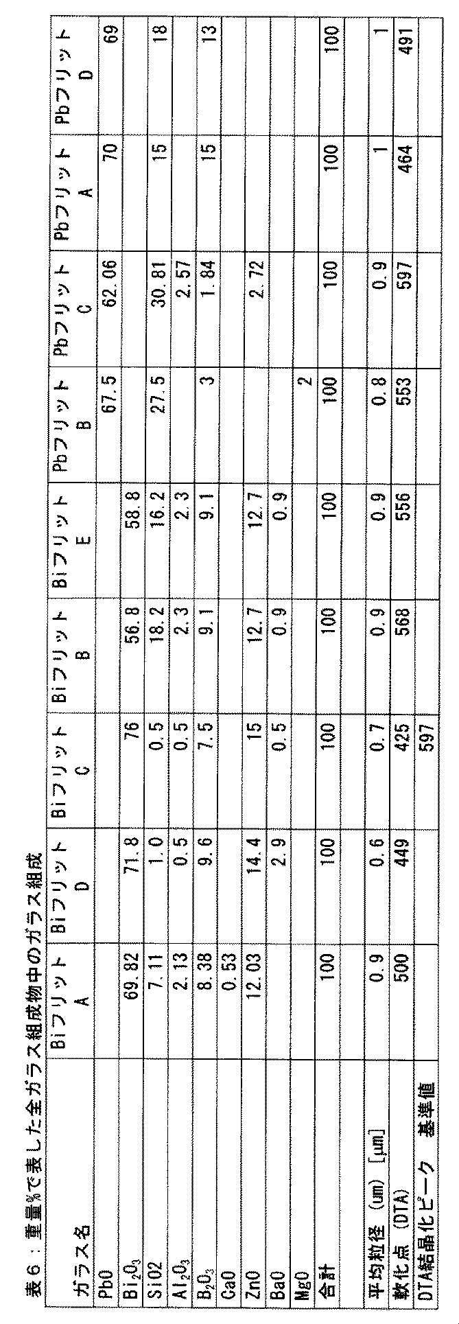
適用実施例1および比較例1〜4
Ru混合物Aおよび黒色粉末Aを、種々のガラス粉末と混合して、表7に列挙するペースト組成物を製造した。前述の操作(I)および(II)を実施して、各適用実施例および対照例ごとに試験サンプルを製造した。
Application Example 1 and Comparative Examples 1 to 4
Ru mixture A and black powder A were mixed with various glass powders to produce paste compositions listed in Table 7. The above operations (I) and (II) were carried out to produce test samples for each application example and control example.
結果
結果を表8に示す。
Results The results are shown in Table 8.
前述の適用実施例および対照例からわかるように、本発明の鉛フリーの黒色導電性組成物は、所望の特徴を、黒色電極特性の良好なバランスと共に維持することができる。特に、適用実施例1では、繰り返し焼成した後の接触抵抗(表8のオーム抵抗)が最低であり、L値も最低である。 As can be seen from the foregoing application examples and control examples, the lead-free black conductive composition of the present invention can maintain the desired characteristics with a good balance of black electrode properties. In particular, in Application Example 1, the contact resistance after repeated firing (ohm resistance in Table 8) is the lowest, and the L value is also the lowest.
X線回折の結果
実施例1のみが、許容される電極性能を、特に低いオーム抵抗で示している。
X-ray diffraction results Only Example 1 demonstrates acceptable electrode performance, especially with low ohmic resistance.
実施例1は、500℃、550℃、および600℃で焼成した後、結合剤相に存在する結晶を有し、すなわち結晶は、500℃から600℃までの全範囲にわたって存在する。 Example 1 has crystals present in the binder phase after firing at 500 ° C., 550 ° C., and 600 ° C., ie the crystals are present over the entire range from 500 ° C. to 600 ° C.
実施例1は、本発明の範囲内に明らかに包含される。 Example 1 is clearly included within the scope of the present invention.
対照例のすべては、許容できないオーム抵抗を有している。いくつかの対照例は、いくつかの特定の温度で焼成した後に、結合剤相に存在する結晶を有するが、これらは、500℃から600℃の間のすべての温度で結合剤相中に結晶を有しておらず、したがって本発明の範囲に包含されない。 All of the controls have unacceptable ohmic resistance. Some control examples have crystals present in the binder phase after firing at some specific temperature, but these are crystals in the binder phase at all temperatures between 500 ° C and 600 ° C. Are not included in the scope of the present invention.
適用実施例2〜4および対照例5〜12
黒色ペースト3(BiフリットCをベースにする)の接触抵抗性能の再現性を評価するために、黒色ペースト3を、さらに3種のAgペースト(Ag−2、Ag−3、およびAg−4、それぞれ実施例2、3および4)との2層構造において試験をした。実施例2〜4では、プロフィルの長さを2.5時間に延ばした(これに対し実施例1では1.5時間)。
Application Examples 2-4 and Control Examples 5-12
In order to evaluate the reproducibility of the contact resistance performance of the black paste 3 (based on Bi frit C), the black paste 3 was further divided into three types of Ag pastes (Ag-2, Ag-3, and Ag-4, Tests were carried out in a two-layer structure with Examples 2, 3 and 4) respectively. In Examples 2-4, the profile length was increased to 2.5 hours (as opposed to 1.5 hours in Example 1).
比較のため、黒色ペースト1、2、4、および5(上記対照例1〜4で使用)と黒色ペースト6(BiフリットEをベースにする)も含めた(対照例5〜12)。
For comparison,
結果
結果を表9に示す。
Results The results are shown in Table 9.
2層試験で使用されるAg導体とは無関係に、黒色ペースト3(BiフリットCをベースにする)のオーム抵抗性能は、焼成プロフィルがより長い場合であっても良好である。 Regardless of the Ag conductor used in the two-layer test, the ohmic resistance performance of black paste 3 (based on Bi frit C) is good even when the firing profile is longer.
その他のBiフリットをベースにする黒色ペーストは、不十分なオーム抵抗性能を一貫して示している。 Other black pastes based on Bi frit consistently show poor ohmic resistance performance.
適用実施例5〜11および対照例13〜15
実施例5〜11および対照例13〜15の目的は、許容されるオーム抵抗性能を黒色ペースト組成物に与えるために、Bi−フリットC(上記実施例1〜4で十分に機能する)をBi−フリットD(上記対照例で十分に機能しない)と配合することができるかどうか調査することであった。
Application Examples 5-11 and Control Examples 13-15
The purpose of Examples 5-11 and Controls 13-15 was to use Bi-frit C (which works well in Examples 1-4 above) to provide acceptable ohmic resistance performance to the black paste composition. It was to investigate if it could be formulated with frit D (not working well in the above control).
実施例5〜11および対照例13〜15は、1.5時間の長さのプロフィルを使用して焼成した。 Examples 5-11 and Controls 13-15 were fired using a 1.5 hour long profile.
結果
結果を表10に示す。
Results The results are shown in Table 10.
表10の結果は、BiフリットDとBiフリットCとのブレンドからなる黒色ペーストが、特にBiフリットCのレベルが高い場合に、許容されるオーム抵抗性能を与えることができることを示す。 The results in Table 10 show that a black paste consisting of a blend of Bi frit D and Bi frit C can provide acceptable ohmic resistance performance, especially when the level of Bi frit C is high.
対照例17〜24の目的は、BiフリットBをBiフリットDとブレンドすることによって、許容されるオーム抵抗性能を有する黒色ペースト組成物を得ることができるかどうか(すなわち、個別に使用した場合に黒色ペーストに良好な性能をもたらさない2種のフリットは、これらを混合した場合に十分機能することができるのか)、調査することであった。 The purpose of Control Examples 17-24 was to blend Bi-Frit B with Bi-Frit D to obtain a black paste composition with acceptable ohmic resistance performance (ie when used individually) Two frits that did not give good performance to the black paste could work well when mixed together).
対照例17〜24を、1.5時間の長さのプロフィルを使用して焼成した。 Controls 17-24 were fired using a 1.5 hour long profile.
結果
結果を表11に示す。
Results The results are shown in Table 11.
BiフリットBとBiフリットDとのブレンドによって、不十分な性能が一貫してもたらされる。 The blend of Bi frit B and Bi frit D consistently results in poor performance.
適用実施例12〜14では、黒色電極の膜厚を変化させることによる影響について、評価した。これらの実施例では、乾燥後の膜厚を3〜5μmに変化させた。得られた結果を表12に示す。 In application examples 12 to 14, the effect of changing the film thickness of the black electrode was evaluated. In these examples, the film thickness after drying was changed to 3 to 5 μm. The results obtained are shown in Table 12.
接触抵抗性能は、黒色層の厚さとは無関係に維持される。 Contact resistance performance is maintained regardless of the thickness of the black layer.
1 透明電極
2 アドレス電極
3 蛍光材料
4 セル障壁
5 前面ガラス基板
6 背面ガラス基板
7 バス導体電極
7a 露光部分
7b 未露光部分
8 誘電体層
9 保護MgO層
10 黒色電極(感光性厚膜電極層)
10a 露光部分
10b 未露光部分
11 MgO層
13 フォトツール(ターゲット)
DESCRIPTION OF
10a
Claims (9)
鉛フリーの黒色導電性組成物を供給するステップであって、該組成物の全重量%に対し、(a)RuO2、1種または複数の鉛フリーのルテニウムをベースにしたポリ酸化物、およびこれらの混合物から選択された4〜30重量%の導電性金属酸化物、(b)10〜50重量%の鉛フリーのビスマスをベースにしたガラス結合剤、および(c)0〜30重量%の鉛フリーの非導電性黒色酸化物を含む鉛フリーの黒色導電性組成物を供給するステップと、
前記黒色導電性組成物を前記基板上に付着させるステップと、
500〜600℃の範囲の温度で焼結して、500〜600℃の焼結範囲全体にわたり結晶化ガラス成分を含んでいる黒色電極を形成するステップと
を含むことを特徴とする、鉛フリーの黒色電極を形成する方法。 Supplying a substrate;
Supplying a lead-free black conductive composition comprising (a) RuO 2 , one or more lead-free ruthenium-based polyoxides, based on the total weight percent of the composition, and 4-30% by weight of conductive metal oxides selected from these mixtures, (b) 10-50% by weight of lead-free bismuth-based glass binder, and (c) 0-30% by weight Providing a lead-free black conductive composition comprising a lead-free non-conductive black oxide;
Depositing the black conductive composition on the substrate;
Sintering at a temperature in the range of 500 to 600 ° C. to form a black electrode containing a crystallized glass component over the entire sintering range of 500 to 600 ° C. A method of forming a black electrode.
A black electrode comprising a crystallized glass component.
Applications Claiming Priority (4)
| Application Number | Priority Date | Filing Date | Title |
|---|---|---|---|
| US65983905P | 2005-03-09 | 2005-03-09 | |
| US60/659,839 | 2005-03-09 | ||
| US11/369,550 US7384577B2 (en) | 2005-03-09 | 2006-03-07 | Black conductive thick film compositions, black electrodes, and methods of forming thereof |
| US11/369,550 | 2006-03-07 |
Publications (2)
| Publication Number | Publication Date |
|---|---|
| JP2006253143A true JP2006253143A (en) | 2006-09-21 |
| JP5080743B2 JP5080743B2 (en) | 2012-11-21 |
Family
ID=36675888
Family Applications (1)
| Application Number | Title | Priority Date | Filing Date |
|---|---|---|---|
| JP2006064794A Expired - Fee Related JP5080743B2 (en) | 2005-03-09 | 2006-03-09 | Black conductive thick film composition, black electrode, and formation method thereof |
Country Status (6)
| Country | Link |
|---|---|
| US (2) | US7384577B2 (en) |
| EP (1) | EP1701372A3 (en) |
| JP (1) | JP5080743B2 (en) |
| KR (1) | KR100768649B1 (en) |
| CN (1) | CN100587888C (en) |
| TW (1) | TW200641960A (en) |
Cited By (10)
| Publication number | Priority date | Publication date | Assignee | Title |
|---|---|---|---|---|
| WO2008129822A1 (en) * | 2007-04-18 | 2008-10-30 | Panasonic Corporation | Plasma display panel |
| JP2008269863A (en) * | 2007-04-18 | 2008-11-06 | Matsushita Electric Ind Co Ltd | Method for manufacturing plasma display panel |
| JP2008269861A (en) * | 2007-04-18 | 2008-11-06 | Matsushita Electric Ind Co Ltd | Plasma display panel |
| JP2008269862A (en) * | 2007-04-18 | 2008-11-06 | Matsushita Electric Ind Co Ltd | Plasma display panel |
| JP2010173904A (en) * | 2009-01-30 | 2010-08-12 | Asahi Glass Co Ltd | Glass composition and conductive paste using the same |
| JP2010536154A (en) * | 2007-08-08 | 2010-11-25 | イー・アイ・デュポン・ドウ・ヌムール・アンド・カンパニー | Electrode paste for plasma display panel and black bus electrode for plasma display panel |
| JP2011503806A (en) * | 2007-11-06 | 2011-01-27 | イー・アイ・デュポン・ドウ・ヌムール・アンド・カンパニー | Conductive composition for black bus electrode and front panel of plasma display panel |
| JP2011213526A (en) * | 2010-03-31 | 2011-10-27 | Nihon Yamamura Glass Co Ltd | Glass composition |
| JP5003481B2 (en) * | 2006-01-12 | 2012-08-15 | 東レ株式会社 | Photosensitive composition, display member and method for producing the same |
| JP2015060091A (en) * | 2013-09-19 | 2015-03-30 | 日立化成株式会社 | Manufacturing method of conductive pattern, conductive pattern substrate including conductive pattern manufactured by the method, touch panel sensor including the conductive pattern substrate, and photosensitive conductive film |
Families Citing this family (21)
| Publication number | Priority date | Publication date | Assignee | Title |
|---|---|---|---|---|
| US7384577B2 (en) * | 2005-03-09 | 2008-06-10 | E.I. Du Pont De Nemours And Company | Black conductive thick film compositions, black electrodes, and methods of forming thereof |
| US7435361B2 (en) * | 2005-04-14 | 2008-10-14 | E.I. Du Pont De Nemours And Company | Conductive compositions and processes for use in the manufacture of semiconductor devices |
| KR100705888B1 (en) * | 2005-08-26 | 2007-04-09 | 제일모직주식회사 | A plasma display panel comprising a non-photosensitive black layer composition and a black layer formed from the composition, and a manufacturing method thereof |
| US7718092B2 (en) * | 2005-10-11 | 2010-05-18 | E.I. Du Pont De Nemours And Company | Aluminum thick film composition(s), electrode(s), semiconductor device(s) and methods of making thereof |
| KR20080047769A (en) * | 2006-11-27 | 2008-05-30 | 삼성에스디아이 주식회사 | A plasma display panel comprising a composition for forming a bus electrode for a plasma display panel, and a bus electrode prepared therefrom |
| JP2008226832A (en) * | 2007-02-16 | 2008-09-25 | Matsushita Electric Ind Co Ltd | Plasma display panel and manufacturing method thereof, and paste for display electrode thereof |
| KR100899197B1 (en) * | 2007-04-18 | 2009-05-26 | 제일모직주식회사 | Plasma display panel comprising a paste composition for forming an electrode comprising a colored glass frit and an electrode manufactured using the same |
| KR100863957B1 (en) | 2007-04-25 | 2008-10-16 | 삼성에스디아이 주식회사 | Composition for forming electrode and plasma display panel manufactured therefrom |
| US7749321B2 (en) * | 2007-06-28 | 2010-07-06 | E. I. Du Pont De Nemours And Company | Black pigment compositions, thick film black pigment compositions, conductive single layer thick film compositions, and black and conductive electrodes formed therefrom |
| JP5303127B2 (en) * | 2007-08-03 | 2013-10-02 | イー・アイ・デュポン・ドウ・ヌムール・アンド・カンパニー | Conductive composition for black bus electrode and front panel of plasma display panel |
| US20090085136A1 (en) * | 2007-09-27 | 2009-04-02 | Chang Eun Lee | Image sensor and method for manufacturing the same |
| US7648655B2 (en) * | 2007-10-30 | 2010-01-19 | E. I. Du Pont De Nemours And Company | Conductive composition for black bus electrode, and front panel of plasma display panel |
| US8329304B2 (en) * | 2008-05-27 | 2012-12-11 | Guardian Industries Corp. | Plasma display panel including TCC EMI filter, and/or method of making the same |
| WO2010055660A1 (en) * | 2008-11-14 | 2010-05-20 | パナソニック株式会社 | Flat panel display manufacturing method |
| CN102044395B (en) * | 2010-12-09 | 2012-08-15 | 东南大学 | Method for directly preparing two-layer electrode by one-time silk-screen printing and used slurry thereof |
| WO2012167921A1 (en) * | 2011-06-10 | 2012-12-13 | Schott Ag | Feedthrough |
| CN103915248B (en) * | 2014-03-27 | 2016-09-28 | 深圳振华富电子有限公司 | The preparation method of base metal termination electrode inducer |
| KR101737207B1 (en) * | 2014-07-11 | 2017-05-29 | 주식회사 엘지화학 | Positive polar meterials and its maufacturing method of secondary battery |
| KR101816236B1 (en) | 2015-04-28 | 2018-01-08 | 삼성에스디아이 주식회사 | Composition forforming electrode, electrode manufactured using the same and solar cell |
| CN107992234A (en) * | 2017-12-29 | 2018-05-04 | 东莞北斗同创智能科技有限公司 | A kind of intelligence wearing touch-screen and its semi-transparent ito film layer manufacturing method thereof |
| TWI798061B (en) * | 2022-04-19 | 2023-04-01 | 華新科技股份有限公司 | Lead-free thick film resistor composition and lead-free thick film resistor |
Citations (13)
| Publication number | Priority date | Publication date | Assignee | Title |
|---|---|---|---|---|
| JPS60145949A (en) * | 1984-01-06 | 1985-08-01 | 昭栄化学工業株式会社 | Resistor composition |
| JPH10139478A (en) * | 1996-02-15 | 1998-05-26 | Asahi Glass Co Ltd | Sealing composition |
| JPH10194778A (en) * | 1997-01-07 | 1998-07-28 | Namitsukusu Kk | Conductive fired body and gas discharge display panel using the same |
| JPH10255670A (en) * | 1997-03-06 | 1998-09-25 | E I Du Pont De Nemours & Co | Plasma display panel device and its manufacture |
| JPH1116499A (en) * | 1997-06-26 | 1999-01-22 | Toray Ind Inc | Plasma display and method of manufacturing the same |
| JP2000221671A (en) * | 1999-01-29 | 2000-08-11 | Taiyo Ink Mfg Ltd | Photosetting electrically conductive composition and plasma display panel with electrode formed using same |
| JP2000260336A (en) * | 1999-01-06 | 2000-09-22 | Toray Ind Inc | Display substrate and method of manufacturing the same |
| JP2002313226A (en) * | 2001-04-12 | 2002-10-25 | Fujitsu Ltd | Electrode forming method and electrode material for thin display device |
| JP2002373592A (en) * | 2001-06-14 | 2002-12-26 | Matsushita Electric Ind Co Ltd | Electrode for plasma display panel and method of manufacturing the same |
| JP2003016928A (en) * | 2001-07-05 | 2003-01-17 | Matsushita Electric Ind Co Ltd | Plasma display panel and method of manufacturing the same |
| JP2003128430A (en) * | 2001-10-22 | 2003-05-08 | Asahi Techno Glass Corp | Lead-free glass composition |
| JP2004238273A (en) * | 2002-03-29 | 2004-08-26 | Matsushita Electric Ind Co Ltd | Bismuth-based glass composition, and magnetic head and plasma display panel using the same as sealing member |
| JP2004335226A (en) * | 2003-05-06 | 2004-11-25 | Sumitomo Rubber Ind Ltd | Front electrode for plasma display panel and method of manufacturing the same |
Family Cites Families (39)
| Publication number | Priority date | Publication date | Assignee | Title |
|---|---|---|---|---|
| BE525225A (en) * | 1951-08-20 | |||
| US2850445A (en) * | 1955-01-19 | 1958-09-02 | Oster Gerald | Photopolymerization |
| US2875047A (en) * | 1955-01-19 | 1959-02-24 | Oster Gerald | Photopolymerization with the formation of coherent plastic masses |
| NL218803A (en) * | 1956-07-09 | |||
| US3074974A (en) * | 1957-12-06 | 1963-01-22 | Monsanto Chemicals | Method for the preparation of diglycidyl ether of tetrachlorobisphenol-a |
| US3097097A (en) * | 1959-02-12 | 1963-07-09 | Gisela K Oster | Photo degrading of gel systems and photographic production of reliefs therewith |
| NL254306A (en) * | 1959-08-07 | |||
| GB1090142A (en) * | 1965-02-26 | 1967-11-08 | Agfa Gevaert Nv | Photochemical insolubilisation of polymers |
| US3479185A (en) | 1965-06-03 | 1969-11-18 | Du Pont | Photopolymerizable compositions and layers containing 2,4,5-triphenylimidazoyl dimers |
| US3380381A (en) * | 1965-08-06 | 1968-04-30 | Western Printing Mach Co | Rotary press printing cylinder for clamping flexible plates |
| US3479186A (en) * | 1966-01-27 | 1969-11-18 | Polaroid Corp | Emulsion binders |
| US3549367A (en) * | 1968-05-24 | 1970-12-22 | Du Pont | Photopolymerizable compositions containing triarylimidazolyl dimers and p-aminophenyl ketones |
| US3583931A (en) * | 1969-11-26 | 1971-06-08 | Du Pont | Oxides of cubic crystal structure containing bismuth and at least one of ruthenium and iridium |
| US4162162A (en) * | 1978-05-08 | 1979-07-24 | E. I. Du Pont De Nemours And Company | Derivatives of aryl ketones and p-dialkyl-aminoarylaldehydes as visible sensitizers of photopolymerizable compositions |
| US4476039A (en) * | 1983-01-21 | 1984-10-09 | E. I. Du Pont De Nemours And Company | Stain-resistant ruthenium oxide-based resistors |
| US5032490A (en) * | 1989-08-21 | 1991-07-16 | E. I. Du Pont De Nemours And Company | Photosensitive aqueous developable copper conductor composition |
| US5252521A (en) * | 1992-10-19 | 1993-10-12 | Ferro Corporation | Bismuth-containing lead-free glass enamels and glazes of low silica content |
| US5378408A (en) * | 1993-07-29 | 1995-01-03 | E. I. Du Pont De Nemours And Company | Lead-free thick film paste composition |
| US5491118A (en) * | 1994-12-20 | 1996-02-13 | E. I. Du Pont De Nemours And Company | Cadmium-free and lead-free thick film paste composition |
| JPH1073233A (en) | 1996-08-30 | 1998-03-17 | Mitsui Eng & Shipbuild Co Ltd | Water cooling system for molten slag of combustion melting furnace |
| JP3510761B2 (en) | 1997-03-26 | 2004-03-29 | 太陽インキ製造株式会社 | Alkali-developing photocurable conductive paste composition and plasma display panel formed with electrodes using the same |
| JP3541125B2 (en) | 1998-05-01 | 2004-07-07 | 太陽インキ製造株式会社 | Alkali-developing photocurable conductive paste composition and plasma display panel formed with electrodes using the same |
| JP4013340B2 (en) * | 1998-06-30 | 2007-11-28 | 東レ株式会社 | Plasma display components |
| KR100369565B1 (en) * | 1999-12-17 | 2003-01-29 | 대주정밀화학 주식회사 | Resistive paste composition for the formation of electrically heat-generating layer |
| FR2803945A1 (en) | 2000-01-17 | 2001-07-20 | Thomson Plasma | Paste for production of electrodes on a glass substrate enabling lower firing temperatures and a method for the fabrication of a plasma paneled slab or flat visual screens |
| CN100350820C (en) | 2000-06-30 | 2007-11-21 | E·I·内穆尔杜邦公司 | Process for thick film circuit patterning |
| JP3538387B2 (en) | 2001-01-29 | 2004-06-14 | 太陽インキ製造株式会社 | Photocurable resin composition and plasma display panel formed with electrodes using the same |
| RU2185678C1 (en) * | 2001-02-27 | 2002-07-20 | Открытое акционерное общество "Научно-исследовательский институт газоразрядных приборов "Плазма" | Ac gas panel |
| JP3780945B2 (en) * | 2001-03-14 | 2006-05-31 | 株式会社村田製作所 | Ceramic electronic components |
| GB0108886D0 (en) * | 2001-04-09 | 2001-05-30 | Du Pont | Conductor composition II |
| JP2002367518A (en) | 2001-06-12 | 2002-12-20 | Matsushita Electric Ind Co Ltd | Electrodes for plasma display panels, plasma display panels |
| US20030124461A1 (en) * | 2001-10-12 | 2003-07-03 | Suess Terry R. | Aqueous developable photoimageable thick film compositions for making photoimageable black electrodes |
| US20050014091A1 (en) * | 2001-10-12 | 2005-01-20 | Smith Jerome David | Aqueous developable photoimageable thick film compositions for making photoimageable black electrodes |
| JP3538408B2 (en) | 2001-10-23 | 2004-06-14 | 太陽インキ製造株式会社 | Photocurable composition and plasma display panel formed with electrodes using the same |
| JP3918992B2 (en) | 2002-01-30 | 2007-05-23 | 株式会社日立プラズマパテントライセンシング | Method for manufacturing rear substrate for plasma display panel |
| CN1286753C (en) * | 2002-03-29 | 2006-11-29 | 松下电器产业株式会社 | Bismuth glass composition, and magnetic head and plasma display panel including the same as sealing member |
| JP2004190037A (en) * | 2004-01-21 | 2004-07-08 | Taiyo Ink Mfg Ltd | Photocurable resin composition |
| US7384577B2 (en) * | 2005-03-09 | 2008-06-10 | E.I. Du Pont De Nemours And Company | Black conductive thick film compositions, black electrodes, and methods of forming thereof |
| US7214466B1 (en) * | 2005-12-14 | 2007-05-08 | E. I. Du Pont De Nemours And Company | Cationically polymerizable photoimageable thick film compositions, electrodes, and methods of forming thereof |
-
2006
- 2006-03-07 US US11/369,550 patent/US7384577B2/en not_active Expired - Fee Related
- 2006-03-09 KR KR1020060022436A patent/KR100768649B1/en not_active Expired - Fee Related
- 2006-03-09 CN CN200610082025A patent/CN100587888C/en not_active Expired - Fee Related
- 2006-03-09 JP JP2006064794A patent/JP5080743B2/en not_active Expired - Fee Related
- 2006-03-09 TW TW095108036A patent/TW200641960A/en unknown
- 2006-03-09 EP EP06251262A patent/EP1701372A3/en not_active Withdrawn
-
2008
- 2008-03-10 US US12/075,354 patent/US20080157033A1/en not_active Abandoned
Patent Citations (13)
| Publication number | Priority date | Publication date | Assignee | Title |
|---|---|---|---|---|
| JPS60145949A (en) * | 1984-01-06 | 1985-08-01 | 昭栄化学工業株式会社 | Resistor composition |
| JPH10139478A (en) * | 1996-02-15 | 1998-05-26 | Asahi Glass Co Ltd | Sealing composition |
| JPH10194778A (en) * | 1997-01-07 | 1998-07-28 | Namitsukusu Kk | Conductive fired body and gas discharge display panel using the same |
| JPH10255670A (en) * | 1997-03-06 | 1998-09-25 | E I Du Pont De Nemours & Co | Plasma display panel device and its manufacture |
| JPH1116499A (en) * | 1997-06-26 | 1999-01-22 | Toray Ind Inc | Plasma display and method of manufacturing the same |
| JP2000260336A (en) * | 1999-01-06 | 2000-09-22 | Toray Ind Inc | Display substrate and method of manufacturing the same |
| JP2000221671A (en) * | 1999-01-29 | 2000-08-11 | Taiyo Ink Mfg Ltd | Photosetting electrically conductive composition and plasma display panel with electrode formed using same |
| JP2002313226A (en) * | 2001-04-12 | 2002-10-25 | Fujitsu Ltd | Electrode forming method and electrode material for thin display device |
| JP2002373592A (en) * | 2001-06-14 | 2002-12-26 | Matsushita Electric Ind Co Ltd | Electrode for plasma display panel and method of manufacturing the same |
| JP2003016928A (en) * | 2001-07-05 | 2003-01-17 | Matsushita Electric Ind Co Ltd | Plasma display panel and method of manufacturing the same |
| JP2003128430A (en) * | 2001-10-22 | 2003-05-08 | Asahi Techno Glass Corp | Lead-free glass composition |
| JP2004238273A (en) * | 2002-03-29 | 2004-08-26 | Matsushita Electric Ind Co Ltd | Bismuth-based glass composition, and magnetic head and plasma display panel using the same as sealing member |
| JP2004335226A (en) * | 2003-05-06 | 2004-11-25 | Sumitomo Rubber Ind Ltd | Front electrode for plasma display panel and method of manufacturing the same |
Cited By (10)
| Publication number | Priority date | Publication date | Assignee | Title |
|---|---|---|---|---|
| JP5003481B2 (en) * | 2006-01-12 | 2012-08-15 | 東レ株式会社 | Photosensitive composition, display member and method for producing the same |
| WO2008129822A1 (en) * | 2007-04-18 | 2008-10-30 | Panasonic Corporation | Plasma display panel |
| JP2008269863A (en) * | 2007-04-18 | 2008-11-06 | Matsushita Electric Ind Co Ltd | Method for manufacturing plasma display panel |
| JP2008269861A (en) * | 2007-04-18 | 2008-11-06 | Matsushita Electric Ind Co Ltd | Plasma display panel |
| JP2008269862A (en) * | 2007-04-18 | 2008-11-06 | Matsushita Electric Ind Co Ltd | Plasma display panel |
| JP2010536154A (en) * | 2007-08-08 | 2010-11-25 | イー・アイ・デュポン・ドウ・ヌムール・アンド・カンパニー | Electrode paste for plasma display panel and black bus electrode for plasma display panel |
| JP2011503806A (en) * | 2007-11-06 | 2011-01-27 | イー・アイ・デュポン・ドウ・ヌムール・アンド・カンパニー | Conductive composition for black bus electrode and front panel of plasma display panel |
| JP2010173904A (en) * | 2009-01-30 | 2010-08-12 | Asahi Glass Co Ltd | Glass composition and conductive paste using the same |
| JP2011213526A (en) * | 2010-03-31 | 2011-10-27 | Nihon Yamamura Glass Co Ltd | Glass composition |
| JP2015060091A (en) * | 2013-09-19 | 2015-03-30 | 日立化成株式会社 | Manufacturing method of conductive pattern, conductive pattern substrate including conductive pattern manufactured by the method, touch panel sensor including the conductive pattern substrate, and photosensitive conductive film |
Also Published As
| Publication number | Publication date |
|---|---|
| KR20060099444A (en) | 2006-09-19 |
| TW200641960A (en) | 2006-12-01 |
| CN1848355A (en) | 2006-10-18 |
| US7384577B2 (en) | 2008-06-10 |
| CN100587888C (en) | 2010-02-03 |
| JP5080743B2 (en) | 2012-11-21 |
| KR100768649B1 (en) | 2007-10-18 |
| EP1701372A2 (en) | 2006-09-13 |
| EP1701372A3 (en) | 2008-12-03 |
| US20080157033A1 (en) | 2008-07-03 |
| US20060216529A1 (en) | 2006-09-28 |
Similar Documents
| Publication | Publication Date | Title |
|---|---|---|
| JP5080743B2 (en) | Black conductive thick film composition, black electrode, and formation method thereof | |
| JP3779297B2 (en) | Photoformable black electrode and black electrode composition | |
| KR100719016B1 (en) | Photosensitive Thick-Film Paste Materials for Forming Light-Transmitting Electromagnetic Shields, Light-Transmitting Electromagnetic Shields Formed Using the Same, and Method of Manufacture Thereof | |
| KR101100490B1 (en) | Electrode Paste for Plasma Display Panel and Black Bus Electrode for Plasma Display Panel | |
| US7678296B2 (en) | Black conductive thick film compositions, black electrodes, and methods of forming thereof | |
| JP5108239B2 (en) | Black conductive composition, black electrode, and method for forming the same | |
| US7381353B2 (en) | Black conductive thick film compositions, black electrodes, and methods of forming thereof | |
| KR100904145B1 (en) | Black conductive thick film compositions, black electrodes, and methods of forming thereof | |
| US7569165B2 (en) | Black conductive compositions, black electrodes, and methods of forming thereof | |
| JP2012513624A (en) | Photosensitive paste and pattern production method using the same | |
| US20030124461A1 (en) | Aqueous developable photoimageable thick film compositions for making photoimageable black electrodes | |
| CN101842853A (en) | Conductive composition for black bus electrodes, and front panels of plasma display screens | |
| CN101816047A (en) | Conductive composition for black bus electrode and front panel of plasma display panel | |
| JP5421391B2 (en) | Front electrode of PDP | |
| KR20080090371A (en) | Black conductive thick film composition, black electrode and manufacturing method thereof | |
| US20050014091A1 (en) | Aqueous developable photoimageable thick film compositions for making photoimageable black electrodes | |
| JP2014063705A (en) | Method of manufacturing pdp bus electrode |
Legal Events
| Date | Code | Title | Description |
|---|---|---|---|
| A621 | Written request for application examination |
Free format text: JAPANESE INTERMEDIATE CODE: A621 Effective date: 20090213 |
|
| A977 | Report on retrieval |
Free format text: JAPANESE INTERMEDIATE CODE: A971007 Effective date: 20110623 |
|
| A131 | Notification of reasons for refusal |
Free format text: JAPANESE INTERMEDIATE CODE: A131 Effective date: 20110628 |
|
| A521 | Written amendment |
Free format text: JAPANESE INTERMEDIATE CODE: A523 Effective date: 20110928 |
|
| A131 | Notification of reasons for refusal |
Free format text: JAPANESE INTERMEDIATE CODE: A131 Effective date: 20120207 |
|
| A521 | Written amendment |
Free format text: JAPANESE INTERMEDIATE CODE: A523 Effective date: 20120416 |
|
| TRDD | Decision of grant or rejection written | ||
| A01 | Written decision to grant a patent or to grant a registration (utility model) |
Free format text: JAPANESE INTERMEDIATE CODE: A01 Effective date: 20120803 |
|
| A01 | Written decision to grant a patent or to grant a registration (utility model) |
Free format text: JAPANESE INTERMEDIATE CODE: A01 |
|
| A61 | First payment of annual fees (during grant procedure) |
Free format text: JAPANESE INTERMEDIATE CODE: A61 Effective date: 20120831 |
|
| FPAY | Renewal fee payment (event date is renewal date of database) |
Free format text: PAYMENT UNTIL: 20150907 Year of fee payment: 3 |
|
| R150 | Certificate of patent or registration of utility model |
Free format text: JAPANESE INTERMEDIATE CODE: R150 |
|
| LAPS | Cancellation because of no payment of annual fees |