JP2006261402A - 光電変換膜積層型カラー固体撮像素子 - Google Patents
光電変換膜積層型カラー固体撮像素子 Download PDFInfo
- Publication number
- JP2006261402A JP2006261402A JP2005077038A JP2005077038A JP2006261402A JP 2006261402 A JP2006261402 A JP 2006261402A JP 2005077038 A JP2005077038 A JP 2005077038A JP 2005077038 A JP2005077038 A JP 2005077038A JP 2006261402 A JP2006261402 A JP 2006261402A
- Authority
- JP
- Japan
- Prior art keywords
- light
- photoelectric conversion
- conversion film
- silicon substrate
- imaging device
- Prior art date
- Legal status (The legal status is an assumption and is not a legal conclusion. Google has not performed a legal analysis and makes no representation as to the accuracy of the status listed.)
- Granted
Links
Images



Classifications
-
- H—ELECTRICITY
- H10—SEMICONDUCTOR DEVICES; ELECTRIC SOLID-STATE DEVICES NOT OTHERWISE PROVIDED FOR
- H10F—INORGANIC SEMICONDUCTOR DEVICES SENSITIVE TO INFRARED RADIATION, LIGHT, ELECTROMAGNETIC RADIATION OF SHORTER WAVELENGTH OR CORPUSCULAR RADIATION
- H10F39/00—Integrated devices, or assemblies of multiple devices, comprising at least one element covered by group H10F30/00, e.g. radiation detectors comprising photodiode arrays
- H10F39/10—Integrated devices
- H10F39/12—Image sensors
- H10F39/18—Complementary metal-oxide-semiconductor [CMOS] image sensors; Photodiode array image sensors
- H10F39/182—Colour image sensors
-
- H—ELECTRICITY
- H10—SEMICONDUCTOR DEVICES; ELECTRIC SOLID-STATE DEVICES NOT OTHERWISE PROVIDED FOR
- H10F—INORGANIC SEMICONDUCTOR DEVICES SENSITIVE TO INFRARED RADIATION, LIGHT, ELECTROMAGNETIC RADIATION OF SHORTER WAVELENGTH OR CORPUSCULAR RADIATION
- H10F39/00—Integrated devices, or assemblies of multiple devices, comprising at least one element covered by group H10F30/00, e.g. radiation detectors comprising photodiode arrays
- H10F39/80—Constructional details of image sensors
- H10F39/805—Coatings
- H10F39/8053—Colour filters
-
- H—ELECTRICITY
- H10—SEMICONDUCTOR DEVICES; ELECTRIC SOLID-STATE DEVICES NOT OTHERWISE PROVIDED FOR
- H10F—INORGANIC SEMICONDUCTOR DEVICES SENSITIVE TO INFRARED RADIATION, LIGHT, ELECTROMAGNETIC RADIATION OF SHORTER WAVELENGTH OR CORPUSCULAR RADIATION
- H10F39/00—Integrated devices, or assemblies of multiple devices, comprising at least one element covered by group H10F30/00, e.g. radiation detectors comprising photodiode arrays
- H10F39/80—Constructional details of image sensors
- H10F39/806—Optical elements or arrangements associated with the image sensors
-
- H—ELECTRICITY
- H10—SEMICONDUCTOR DEVICES; ELECTRIC SOLID-STATE DEVICES NOT OTHERWISE PROVIDED FOR
- H10K—ORGANIC ELECTRIC SOLID-STATE DEVICES
- H10K30/00—Organic devices sensitive to infrared radiation, light, electromagnetic radiation of shorter wavelength or corpuscular radiation
- H10K30/20—Organic devices sensitive to infrared radiation, light, electromagnetic radiation of shorter wavelength or corpuscular radiation comprising organic-organic junctions, e.g. donor-acceptor junctions
-
- H—ELECTRICITY
- H10—SEMICONDUCTOR DEVICES; ELECTRIC SOLID-STATE DEVICES NOT OTHERWISE PROVIDED FOR
- H10K—ORGANIC ELECTRIC SOLID-STATE DEVICES
- H10K39/00—Integrated devices, or assemblies of multiple devices, comprising at least one organic radiation-sensitive element covered by group H10K30/00
- H10K39/30—Devices controlled by radiation
- H10K39/32—Organic image sensors
Landscapes
- Solid State Image Pick-Up Elements (AREA)
- Light Receiving Elements (AREA)
Abstract
【解決手段】 シリコン基板101の上層に緑色光を吸収して光電荷を発生させる光電変換膜10を積層すると共にシリコン基板101の深さ方向の浅部と深部とに夫々フォトダイオードを形成し、シリコンの光吸収係数の波長依存性により該シリコン基板に浸入する光を青色光と赤色光の2色に分離し、シリコン基板101の浅部で発生した光電荷を浅部のフォトダイオードで検出してこれを青色光による信号とし、シリコン基板101の深部で発生した光電荷を深部のフォトダイオードで検出してこれを赤色光による信号とする光電変換膜積層型カラー固体撮像素子において、光電変換膜10とシリコン基板101との間に、光電変換膜10を透過しフォトダイオードに入射する光の各色光強度を調整するトリミング層111を設ける。
【選択図】 図5
Description
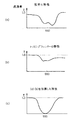
本発明の光電変換膜積層型カラー固体撮像素子の前記トリミング層は、前記光電変換膜を透過し該トリミング層を透過した光の分光感度特性が、波長500nmから波長600nmの間をピークとし半値幅が80nm以下となる材料で形成されることを特徴とする。
本発明の光電変換膜積層型カラー固体撮像素子の前記トリミング層は、前記光電変換膜を透過し該トリミング層を透過した光の分光感度特性が、波長550をピークとし半値幅が50nm以下となる材料で形成されることを特徴とする。
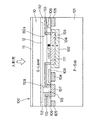
11 共通電極膜
12 画素電極膜
100 ハイブリッド型の光電変換膜積層型カラー固体撮像素子
101 半導体基板
103 n型半導体層
104 P型半導体層
107 緑色用の信号電荷蓄積領域
111 トリミング層
113 縦配線
Claims (3)
- シリコン基板の上層に緑色光を吸収して光電荷を発生させる光電変換膜を積層すると共に該シリコン基板の深さ方向の浅部と深部とに夫々フォトダイオードを形成し、シリコンの光吸収係数の波長依存性により該シリコン基板に浸入する光を青色光と赤色光の2色に分離し、該シリコン基板の浅部で発生した光電荷を前記浅部のフォトダイオードで検出してこれを青色光による信号とし、前記シリコン基板の深部で発生した光電荷を前記深部のフォトダイオードで検出してこれを赤色光による信号とする光電変換膜積層型カラー固体撮像素子において、前記光電変換膜と前記シリコン基板との間に、該光電変換膜を透過し前記フォトダイオードに入射する光の各色光強度を調整するトリミング層を設けたことを特徴とする光電変換膜積層型カラー固体撮像素子。
- 前記トリミング層は、前記光電変換膜を透過し該トリミング層を透過した光の分光感度特性が、波長500nmから波長600nmの間をピークとし半値幅が80nm以下となる材料で形成されることを特徴とする請求項1に記載の光電変換膜積層型カラー固体撮像素子。
- 前記トリミング層は、前記光電変換膜を透過し該トリミング層を透過した光の分光感度特性が、波長550をピークとし半値幅が50nm以下となる材料で形成されることを特徴とする請求項2に記載の光電変換膜積層型カラー固体撮像素子。
Priority Applications (2)
| Application Number | Priority Date | Filing Date | Title |
|---|---|---|---|
| JP2005077038A JP4580789B2 (ja) | 2005-03-17 | 2005-03-17 | 光電変換膜積層型カラー固体撮像素子 |
| US11/377,408 US7230226B2 (en) | 2005-03-17 | 2006-03-17 | Photoelectric conversion layer stack type color solid-state image sensing device |
Applications Claiming Priority (1)
| Application Number | Priority Date | Filing Date | Title |
|---|---|---|---|
| JP2005077038A JP4580789B2 (ja) | 2005-03-17 | 2005-03-17 | 光電変換膜積層型カラー固体撮像素子 |
Publications (2)
| Publication Number | Publication Date |
|---|---|
| JP2006261402A true JP2006261402A (ja) | 2006-09-28 |
| JP4580789B2 JP4580789B2 (ja) | 2010-11-17 |
Family
ID=37009345
Family Applications (1)
| Application Number | Title | Priority Date | Filing Date |
|---|---|---|---|
| JP2005077038A Expired - Fee Related JP4580789B2 (ja) | 2005-03-17 | 2005-03-17 | 光電変換膜積層型カラー固体撮像素子 |
Country Status (2)
| Country | Link |
|---|---|
| US (1) | US7230226B2 (ja) |
| JP (1) | JP4580789B2 (ja) |
Cited By (3)
| Publication number | Priority date | Publication date | Assignee | Title |
|---|---|---|---|---|
| JP2009130239A (ja) * | 2007-11-27 | 2009-06-11 | Nippon Hoso Kyokai <Nhk> | カラー撮像装置 |
| WO2014112279A1 (ja) * | 2013-01-16 | 2014-07-24 | ソニー株式会社 | 固体撮像素子および電子機器 |
| WO2020080072A1 (ja) * | 2018-10-17 | 2020-04-23 | パナソニックIpマネジメント株式会社 | 光電変換素子およびイメージセンサ |
Families Citing this family (10)
| Publication number | Priority date | Publication date | Assignee | Title |
|---|---|---|---|---|
| JP4538353B2 (ja) * | 2005-03-25 | 2010-09-08 | 富士フイルム株式会社 | 光電変換膜積層型カラー固体撮像素子 |
| JP4839008B2 (ja) * | 2005-03-28 | 2011-12-14 | 富士フイルム株式会社 | 単板式カラー固体撮像素子 |
| JP4887079B2 (ja) * | 2006-06-06 | 2012-02-29 | 富士フイルム株式会社 | 光電変換膜積層型固体撮像素子 |
| JP4413940B2 (ja) * | 2007-03-22 | 2010-02-10 | 株式会社東芝 | 固体撮像素子、単板カラー固体撮像素子及び電子機器 |
| US7687836B2 (en) * | 2007-05-24 | 2010-03-30 | Micron Technology, Inc. | Capacitance noise shielding plane for imager sensor devices |
| JP2009010075A (ja) * | 2007-06-27 | 2009-01-15 | Fujifilm Corp | 放射線画像検出器 |
| CN102244083B (zh) * | 2010-05-13 | 2015-08-26 | 博立多媒体控股有限公司 | 一种混合多光谱感光象素组、感光器件、及感光系统 |
| US8912615B2 (en) * | 2013-01-24 | 2014-12-16 | Osi Optoelectronics, Inc. | Shallow junction photodiode for detecting short wavelength light |
| WO2022043894A1 (en) * | 2020-08-26 | 2022-03-03 | Senbiosys | Stacked oximeter and operation method |
| CN112599502B (zh) * | 2020-12-08 | 2023-11-24 | 武汉新芯集成电路制造有限公司 | 多层晶圆的制备方法 |
Citations (5)
| Publication number | Priority date | Publication date | Assignee | Title |
|---|---|---|---|---|
| JPH03120764A (ja) * | 1989-10-03 | 1991-05-22 | Nec Corp | 光センサ |
| JP2003332551A (ja) * | 2002-05-08 | 2003-11-21 | Canon Inc | カラー撮像素子及びカラー受光素子 |
| JP2004165242A (ja) * | 2002-11-11 | 2004-06-10 | Canon Inc | カラー撮像素子及びカラー受光素子 |
| JP2004281773A (ja) * | 2003-03-17 | 2004-10-07 | Fuji Film Microdevices Co Ltd | Mos型カラー固体撮像装置 |
| JP2006203457A (ja) * | 2005-01-19 | 2006-08-03 | Fuji Photo Film Co Ltd | カラー画像生成方法 |
Family Cites Families (5)
| Publication number | Priority date | Publication date | Assignee | Title |
|---|---|---|---|---|
| AU2492399A (en) | 1998-02-02 | 1999-08-16 | Uniax Corporation | Image sensors made from organic semiconductors |
| US5965875A (en) | 1998-04-24 | 1999-10-12 | Foveon, Inc. | Color separation in an active pixel cell imaging array using a triple-well structure |
| JP2002083946A (ja) | 2000-09-07 | 2002-03-22 | Nippon Hoso Kyokai <Nhk> | イメージセンサ |
| US6841816B2 (en) * | 2002-03-20 | 2005-01-11 | Foveon, Inc. | Vertical color filter sensor group with non-sensor filter and method for fabricating such a sensor group |
| US7129466B2 (en) | 2002-05-08 | 2006-10-31 | Canon Kabushiki Kaisha | Color image pickup device and color light-receiving device |
-
2005
- 2005-03-17 JP JP2005077038A patent/JP4580789B2/ja not_active Expired - Fee Related
-
2006
- 2006-03-17 US US11/377,408 patent/US7230226B2/en not_active Expired - Fee Related
Patent Citations (5)
| Publication number | Priority date | Publication date | Assignee | Title |
|---|---|---|---|---|
| JPH03120764A (ja) * | 1989-10-03 | 1991-05-22 | Nec Corp | 光センサ |
| JP2003332551A (ja) * | 2002-05-08 | 2003-11-21 | Canon Inc | カラー撮像素子及びカラー受光素子 |
| JP2004165242A (ja) * | 2002-11-11 | 2004-06-10 | Canon Inc | カラー撮像素子及びカラー受光素子 |
| JP2004281773A (ja) * | 2003-03-17 | 2004-10-07 | Fuji Film Microdevices Co Ltd | Mos型カラー固体撮像装置 |
| JP2006203457A (ja) * | 2005-01-19 | 2006-08-03 | Fuji Photo Film Co Ltd | カラー画像生成方法 |
Cited By (19)
| Publication number | Priority date | Publication date | Assignee | Title |
|---|---|---|---|---|
| JP2009130239A (ja) * | 2007-11-27 | 2009-06-11 | Nippon Hoso Kyokai <Nhk> | カラー撮像装置 |
| US10833110B2 (en) | 2013-01-16 | 2020-11-10 | Sony Semicondutor Solutions Corportion | Solid-state image pickup unit and electronic apparatus |
| US11367794B2 (en) | 2013-01-16 | 2022-06-21 | Sony Semiconductor Solutions Corporation | Solid-state image pickup unit and electronic apparatus |
| JPWO2014112279A1 (ja) * | 2013-01-16 | 2017-01-19 | ソニーセミコンダクタソリューションズ株式会社 | 固体撮像素子および電子機器 |
| US9954018B2 (en) | 2013-01-16 | 2018-04-24 | Sony Semiconductor Solutions Corporation | Solid-state image pickup unit and electronic apparatus |
| US10008524B2 (en) | 2013-01-16 | 2018-06-26 | Sony Semiconductor Solutions Corporation | Solid-state image pickup unit and electronic apparatus |
| US10074697B2 (en) | 2013-01-16 | 2018-09-11 | Sony Semiconductor Solutions Corporation | Solid-state image pickup unit and electronic apparatus |
| US12243944B2 (en) | 2013-01-16 | 2025-03-04 | Sony Semiconductor Solutions Corporation | Solid-state image pickup unit and electronic apparatus |
| WO2014112279A1 (ja) * | 2013-01-16 | 2014-07-24 | ソニー株式会社 | 固体撮像素子および電子機器 |
| KR20150106400A (ko) * | 2013-01-16 | 2015-09-21 | 소니 주식회사 | 고체 촬상 소자 및 전자 기기 |
| US11855227B2 (en) | 2013-01-16 | 2023-12-26 | Sony Semiconductor Solutions Corporation | Solid-state image pickup unit and electronic apparatus |
| KR20200139272A (ko) * | 2013-01-16 | 2020-12-11 | 소니 세미컨덕터 솔루션즈 가부시키가이샤 | 고체 촬상 소자 및 전자 기기 |
| KR102333239B1 (ko) * | 2013-01-16 | 2021-12-01 | 소니 세미컨덕터 솔루션즈 가부시키가이샤 | 고체 촬상 소자 및 전자 기기 |
| KR20210146427A (ko) * | 2013-01-16 | 2021-12-03 | 소니 세미컨덕터 솔루션즈 가부시키가이샤 | 고체 촬상 소자 및 전자 기기 |
| KR102189366B1 (ko) * | 2013-01-16 | 2020-12-09 | 소니 세미컨덕터 솔루션즈 가부시키가이샤 | 고체 촬상 소자 및 전자 기기 |
| KR102517997B1 (ko) | 2013-01-16 | 2023-04-06 | 소니 세미컨덕터 솔루션즈 가부시키가이샤 | 고체 촬상 소자 및 전자 기기 |
| JP7365611B2 (ja) | 2018-10-17 | 2023-10-20 | パナソニックIpマネジメント株式会社 | 光電変換素子およびイメージセンサ |
| JPWO2020080072A1 (ja) * | 2018-10-17 | 2021-09-16 | パナソニックIpマネジメント株式会社 | 光電変換素子およびイメージセンサ |
| WO2020080072A1 (ja) * | 2018-10-17 | 2020-04-23 | パナソニックIpマネジメント株式会社 | 光電変換素子およびイメージセンサ |
Also Published As
| Publication number | Publication date |
|---|---|
| JP4580789B2 (ja) | 2010-11-17 |
| US7230226B2 (en) | 2007-06-12 |
| US20060208162A1 (en) | 2006-09-21 |
Similar Documents
| Publication | Publication Date | Title |
|---|---|---|
| US9880057B2 (en) | Visible and near-infrared radiation detector | |
| US9040916B2 (en) | Visible and near-infrared radiation detector | |
| KR101116448B1 (ko) | 고체 촬상 소자 | |
| KR102410028B1 (ko) | 이미지 센서 및 이를 포함하는 전자 장치 | |
| EP3522226B1 (en) | Image sensors and electronic devices | |
| KR100962449B1 (ko) | 광전 변환층 스택 타입 칼라 고상 이미징 장치 | |
| KR101432016B1 (ko) | 다중 스펙트럼 감광소자 | |
| JP4491323B2 (ja) | 光電変換膜積層型カラー固体撮像装置 | |
| US7760254B2 (en) | Single plate-type color solid-state image sensing device | |
| KR102547655B1 (ko) | 이미지 센서 및 이를 포함하는 전자 장치 | |
| KR102632442B1 (ko) | 이미지 센서 및 전자 장치 | |
| JP4580789B2 (ja) | 光電変換膜積層型カラー固体撮像素子 | |
| KR102520573B1 (ko) | 이미지 센서 및 이를 포함하는 전자 장치 | |
| US8319305B2 (en) | Solid-state image sensing apparatus | |
| CN101577287A (zh) | 多层图像传感器 | |
| CN105428379B (zh) | 提高背照式红外图像传感器性能的方法 | |
| IL181274A (en) | Method and apparatus providing single bump, multi-color pixel architecture | |
| US20050212045A1 (en) | Photo-detecting device | |
| US20160142660A1 (en) | Single chip image sensor with both visible light image and ultraviolet light detection ability and the methods to implement the same | |
| JP2016157744A (ja) | 固体撮像素子 | |
| KR20190119970A (ko) | 이미지 센서 및 전자 장치 | |
| KR102129453B1 (ko) | 이미지 센서 및 이를 포함하는 전자 장치 | |
| JP4404561B2 (ja) | Mos型カラー固体撮像装置 | |
| US7579665B2 (en) | Color light receiving device and image pickup device | |
| JP7240833B2 (ja) | 撮像素子 |
Legal Events
| Date | Code | Title | Description |
|---|---|---|---|
| A711 | Notification of change in applicant |
Free format text: JAPANESE INTERMEDIATE CODE: A712 Effective date: 20061124 |
|
| A621 | Written request for application examination |
Free format text: JAPANESE INTERMEDIATE CODE: A621 Effective date: 20070621 |
|
| RD04 | Notification of resignation of power of attorney |
Free format text: JAPANESE INTERMEDIATE CODE: A7424 Effective date: 20071108 |
|
| RD04 | Notification of resignation of power of attorney |
Free format text: JAPANESE INTERMEDIATE CODE: A7424 Effective date: 20071115 |
|
| RD04 | Notification of resignation of power of attorney |
Free format text: JAPANESE INTERMEDIATE CODE: A7424 Effective date: 20071122 |
|
| A977 | Report on retrieval |
Free format text: JAPANESE INTERMEDIATE CODE: A971007 Effective date: 20100521 |
|
| A131 | Notification of reasons for refusal |
Free format text: JAPANESE INTERMEDIATE CODE: A131 Effective date: 20100601 |
|
| A521 | Request for written amendment filed |
Free format text: JAPANESE INTERMEDIATE CODE: A523 Effective date: 20100708 |
|
| TRDD | Decision of grant or rejection written | ||
| A01 | Written decision to grant a patent or to grant a registration (utility model) |
Free format text: JAPANESE INTERMEDIATE CODE: A01 Effective date: 20100803 |
|
| A01 | Written decision to grant a patent or to grant a registration (utility model) |
Free format text: JAPANESE INTERMEDIATE CODE: A01 |
|
| A61 | First payment of annual fees (during grant procedure) |
Free format text: JAPANESE INTERMEDIATE CODE: A61 Effective date: 20100830 |
|
| FPAY | Renewal fee payment (event date is renewal date of database) |
Free format text: PAYMENT UNTIL: 20130903 Year of fee payment: 3 |
|
| R150 | Certificate of patent or registration of utility model |
Free format text: JAPANESE INTERMEDIATE CODE: R150 |
|
| LAPS | Cancellation because of no payment of annual fees |