JP2006289999A - サーマルヘッド、サーマルヘッドの製造方法 - Google Patents
サーマルヘッド、サーマルヘッドの製造方法 Download PDFInfo
- Publication number
- JP2006289999A JP2006289999A JP2006207374A JP2006207374A JP2006289999A JP 2006289999 A JP2006289999 A JP 2006289999A JP 2006207374 A JP2006207374 A JP 2006207374A JP 2006207374 A JP2006207374 A JP 2006207374A JP 2006289999 A JP2006289999 A JP 2006289999A
- Authority
- JP
- Japan
- Prior art keywords
- head
- chip
- thermal head
- wiring board
- wiring
- Prior art date
- Legal status (The legal status is an assumption and is not a legal conclusion. Google has not performed a legal analysis and makes no representation as to the accuracy of the status listed.)
- Granted
Links
- 238000000034 method Methods 0.000 title claims abstract description 46
- 238000004519 manufacturing process Methods 0.000 title claims description 33
- 238000010438 heat treatment Methods 0.000 claims abstract description 73
- 239000000758 substrate Substances 0.000 claims abstract description 70
- 239000004065 semiconductor Substances 0.000 claims abstract description 20
- 230000002093 peripheral effect Effects 0.000 claims description 15
- 230000000149 penetrating effect Effects 0.000 claims description 2
- 230000008569 process Effects 0.000 abstract description 27
- 239000012790 adhesive layer Substances 0.000 description 38
- 239000000919 ceramic Substances 0.000 description 16
- 239000000853 adhesive Substances 0.000 description 10
- 230000001070 adhesive effect Effects 0.000 description 10
- 230000004048 modification Effects 0.000 description 10
- 238000012986 modification Methods 0.000 description 10
- 230000000694 effects Effects 0.000 description 9
- 230000008901 benefit Effects 0.000 description 8
- 238000005520 cutting process Methods 0.000 description 8
- 239000011521 glass Substances 0.000 description 8
- 238000007639 printing Methods 0.000 description 8
- 239000010410 layer Substances 0.000 description 7
- 239000004593 Epoxy Substances 0.000 description 6
- 229920005989 resin Polymers 0.000 description 6
- 239000011347 resin Substances 0.000 description 6
- 238000007789 sealing Methods 0.000 description 6
- 239000010409 thin film Substances 0.000 description 4
- 229910052782 aluminium Inorganic materials 0.000 description 3
- XAGFODPZIPBFFR-UHFFFAOYSA-N aluminium Chemical compound [Al] XAGFODPZIPBFFR-UHFFFAOYSA-N 0.000 description 3
- 229910052751 metal Inorganic materials 0.000 description 3
- 239000002184 metal Substances 0.000 description 3
- 230000002411 adverse Effects 0.000 description 2
- 239000010408 film Substances 0.000 description 2
- 239000012530 fluid Substances 0.000 description 2
- 230000020169 heat generation Effects 0.000 description 2
- 238000005304 joining Methods 0.000 description 2
- 239000000463 material Substances 0.000 description 2
- 230000009467 reduction Effects 0.000 description 2
- 239000004820 Pressure-sensitive adhesive Substances 0.000 description 1
- 239000002131 composite material Substances 0.000 description 1
- 239000003822 epoxy resin Substances 0.000 description 1
- 239000004744 fabric Substances 0.000 description 1
- PCHJSUWPFVWCPO-UHFFFAOYSA-N gold Chemical compound [Au] PCHJSUWPFVWCPO-UHFFFAOYSA-N 0.000 description 1
- 239000010931 gold Substances 0.000 description 1
- 229910052737 gold Inorganic materials 0.000 description 1
- 230000017525 heat dissipation Effects 0.000 description 1
- 239000011159 matrix material Substances 0.000 description 1
- 235000011837 pasties Nutrition 0.000 description 1
- 229920000647 polyepoxide Polymers 0.000 description 1
- 238000004382 potting Methods 0.000 description 1
- 230000001681 protective effect Effects 0.000 description 1
- 238000004080 punching Methods 0.000 description 1
- 238000007650 screen-printing Methods 0.000 description 1
- 239000007779 soft material Substances 0.000 description 1
- 230000006641 stabilisation Effects 0.000 description 1
- 238000011105 stabilization Methods 0.000 description 1
- XLYOFNOQVPJJNP-UHFFFAOYSA-N water Substances O XLYOFNOQVPJJNP-UHFFFAOYSA-N 0.000 description 1
Images






Landscapes
- Electronic Switches (AREA)
Abstract
基板工程の生産性を向上させると共に、実装工程のハンドリング性を向上させ、大幅なコストダウンを図る。
【解決手段】
一方面に発熱体(24)及び該発熱体(24)に接続される電極(25)を有するヘッドチップ20と、前記電極(24)に接続される半導体集積回路(32)とを具備するサーマルヘッド(10)において、前記ヘッドチップ(20)の他方面に接合される配線基板(30)を具備し、前記半導体集積回路32を前記配線基板(30)に搭載してなる。
【選択図】 図6
Description
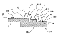
本発明の第10の態様は、第9の態様において、前記ヘッドチップに設けられた共通電極と前記配線基板に設けられた共通電極用配線とを接続する接続配線が、前記半導体集積回路により規定される物理ブロックの間に設けられていることを特徴とするサーマルヘッドにある。
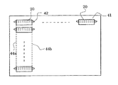
本発明の第19の態様は、第18の態様において、前記ヘッドチップは、前記配線基板用プレートに一方向に向いて縦横複数列ずつ並設されることを特徴とするサーマルヘッドの製造方法にある。
(サーマルヘッドの一実施形態)
図1には、本発明の一実施形態に係るサーマルヘッドの概略断面図及び要部平面図を示す。図1(a)に示すように、サーマルヘッド10は、複数の薄膜層が形成されたヘッドチップ20と、このヘッドチップ20に重ねて接合された配線基板30とを有する。
(製造工程)
以下に、上述したサーマルヘッド10の製造工程の一例を示しながら、さらに詳細に説明する。
(サーマルヘッドユニットの一実施形態)
以上説明したサーマルヘッド10は、アルミニウムなどの金属からなり放熱板の機能を有する支持体に保持してサーマルヘッドユニットとして用いられる。かかるサーマルヘッドユニットの一例を図7(a)に示す。
(サーマルヘッドの他の実施形態)
以上説明したサーマルヘッド10の利点について種々述べてきたが、ヘッドチップ20と配線基板30とを重ね合わせて接合し、配線基板30上にICチップ32を搭載したことにより、従来の構造と比較してICチップ32が相対的に低い位置に配置されているので、封止樹脂35の高さを低くすることができ、これにより、実際にサーマルプリンタ等に搭載したときに被印刷シートの搬送スペースを容易に確保できるという利点がある。すなわち、図9に示すように、発熱体24と対向して配置されるプラテンローラ57と、封止樹脂35との隙間が大きくなるので、被印刷シート58と封止樹脂35との干渉が避けられるという利点がある。
(サーマルヘッドの配線構造)
上述したようなサーマルヘッドにおいて、ヘッドチップ20の小型化を図る場合、例えば、図1に示す共通電極27の幅を最小限に抑える必要がある。通常は、かかる共通電極27は、例えば、両端部で配線基板30上に設けられた共通電極用配線を介して外部端子に接続されて接地されるが、この場合、共通電極27が持つ電気抵抗によって、各発熱体24に流れる電流値にバラツキが生じる。すなわち、共通電極27の接地位置から離れた中央部に接続される発熱体24に流れる電流値は小さくなって発熱量が小さくなり、印字濃度ムラの原因となる。
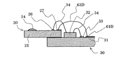
例えば、各物理ブロック内の接続をICチップ32の表面に設けた共通電極用配線61Aを介して行う代わりに、図16に示すように、ICチップ32の下側に設けた共通電極用配線61C及びボンディングワイヤ63Cを介して行ってもよい。この場合、ワイヤボンディングを容易に行うことができ、また、ボンディングワイヤの長さを短くすることができる。
Claims (7)
- 一方面に発熱体及び該発熱体に接続される電極を有するヘッドチップと、前記ヘッドチップの他方面に接合される配線基板とを具備し、半導体集積回路を前記配線基板に搭載してなるサーマルヘッドの製造方法において、前記配線基板を複数個取り可能な配線基板用プレート上に、複数個の前記ヘッドチップを接合する工程と、複数の前記半導体集積回路を前記配線基板用プレートに搭載する工程と、前記ヘッドチップ上の前記電極と前記半導体集積回路とを配線する工程と、前記配線基板用プレートを複数個に分割する工程とを具備することを特徴とするサーマルヘッドの製造方法。
- 請求項1に記載のサーマルヘッドの製造方法において、前記ヘッドチップは、前記配線基板用プレートに一方向に向いて縦横複数列ずつ並設されることを特徴とするサーマルヘッドの製造方法。
- 請求項2に記載のサーマルヘッドの製造方法において、前記ヘッドチップの一部は、前記一方向とは直交する方向に向いて接合されることを特徴とするサーマルヘッドの製造方法。
- 請求項1〜3の何れかに記載のサーマルヘッドの製造方法において、前記配線基板用プレートは、当該プレートを貫通する長孔を有し、当該長孔の内周面が前記配線基板の少なくとも一端面を形成することを特徴とするサーマルヘッドの製造方法。
- 請求項4に記載のサーマルヘッドの製造方法において、前記配線基板用プレートは、一つの前記長孔の内周面が、複数の前記配線基板の少なくとも一端面を形成することを特徴とするサーマルヘッドの製造方法。
- 請求項4又は5に記載のサーマルヘッドの製造方法において、前記ヘッドチップは前記長孔の幅方向両側の周縁部を跨ぎ且つ当該周縁部の何れか一方のみに接合されて設けられることを特徴とするサーマルヘッドの製造方法。
- 一方面に発熱体及び該発熱体に接続される電極を有するヘッドチップと、前記ヘッドチップの他方面に接合される配線基板とを具備し、半導体集積回路を前記配線基板に搭載してなるサーマルヘッドにおいて、前記配線基板には、前記ヘッドチップの他方面の一部分が露出する長孔を有すること、を特徴とするサーマルヘッド。
Priority Applications (1)
| Application Number | Priority Date | Filing Date | Title |
|---|---|---|---|
| JP2006207374A JP4068647B2 (ja) | 1998-08-11 | 2006-07-31 | サーマルヘッドの製造方法 |
Applications Claiming Priority (3)
| Application Number | Priority Date | Filing Date | Title |
|---|---|---|---|
| JP22710498 | 1998-08-11 | ||
| JP23460298 | 1998-08-20 | ||
| JP2006207374A JP4068647B2 (ja) | 1998-08-11 | 2006-07-31 | サーマルヘッドの製造方法 |
Related Parent Applications (1)
| Application Number | Title | Priority Date | Filing Date |
|---|---|---|---|
| JP2000564820A Division JP3905311B2 (ja) | 1998-08-11 | 1999-08-09 | サーマルヘッドユニット、サーマルヘッドの製造方法、及びサーマルヘッドユニットの製造方法 |
Publications (2)
| Publication Number | Publication Date |
|---|---|
| JP2006289999A true JP2006289999A (ja) | 2006-10-26 |
| JP4068647B2 JP4068647B2 (ja) | 2008-03-26 |
Family
ID=37411069
Family Applications (1)
| Application Number | Title | Priority Date | Filing Date |
|---|---|---|---|
| JP2006207374A Expired - Lifetime JP4068647B2 (ja) | 1998-08-11 | 2006-07-31 | サーマルヘッドの製造方法 |
Country Status (1)
| Country | Link |
|---|---|
| JP (1) | JP4068647B2 (ja) |
Cited By (3)
| Publication number | Priority date | Publication date | Assignee | Title |
|---|---|---|---|---|
| JP2013202797A (ja) * | 2012-03-27 | 2013-10-07 | Toshiba Hokuto Electronics Corp | サーマルプリントヘッド |
| JP2016190462A (ja) * | 2015-03-31 | 2016-11-10 | 東芝ホクト電子株式会社 | サーマルプリントヘッド及びサーマルプリンタ |
| JP2018058271A (ja) * | 2016-10-05 | 2018-04-12 | 東芝ホクト電子株式会社 | サーマルプリントヘッド及びその製造方法 |
-
2006
- 2006-07-31 JP JP2006207374A patent/JP4068647B2/ja not_active Expired - Lifetime
Cited By (3)
| Publication number | Priority date | Publication date | Assignee | Title |
|---|---|---|---|---|
| JP2013202797A (ja) * | 2012-03-27 | 2013-10-07 | Toshiba Hokuto Electronics Corp | サーマルプリントヘッド |
| JP2016190462A (ja) * | 2015-03-31 | 2016-11-10 | 東芝ホクト電子株式会社 | サーマルプリントヘッド及びサーマルプリンタ |
| JP2018058271A (ja) * | 2016-10-05 | 2018-04-12 | 東芝ホクト電子株式会社 | サーマルプリントヘッド及びその製造方法 |
Also Published As
| Publication number | Publication date |
|---|---|
| JP4068647B2 (ja) | 2008-03-26 |
Similar Documents
| Publication | Publication Date | Title |
|---|---|---|
| KR100555341B1 (ko) | 반도체장치및그제조방법,회로기판및플렉시블기판 | |
| US6922339B2 (en) | Heat dissipating structure of printed circuit board and fabricating method thereof | |
| US6853089B2 (en) | Semiconductor device and method of manufacturing the same | |
| JP6076675B2 (ja) | 半導体装置 | |
| US20070193027A1 (en) | Method of manufacturing circuit device | |
| JP2000150730A (ja) | 半導体装置及びその製造方法 | |
| JP2001326236A (ja) | 半導体装置の製造方法 | |
| JP4549171B2 (ja) | 混成集積回路装置 | |
| JP3905311B2 (ja) | サーマルヘッドユニット、サーマルヘッドの製造方法、及びサーマルヘッドユニットの製造方法 | |
| JP6480550B2 (ja) | ワイヤボンディング方法、および半導体装置 | |
| JP4975584B2 (ja) | 半導体装置及び半導体装置の製造方法。 | |
| JP4068647B2 (ja) | サーマルヘッドの製造方法 | |
| JPWO2000009341A1 (ja) | サーマルヘッド及びサーマルヘッドユニット並びにその製造方法 | |
| KR100574813B1 (ko) | 열 헤드 및 열 헤드 장치 | |
| JP3923661B2 (ja) | 半導体装置 | |
| JP2714691B2 (ja) | 電子部品搭載用基板の製造方法 | |
| JP4572375B2 (ja) | 半導体装置の製造方法 | |
| JP4036017B2 (ja) | 電子部品の実装構造 | |
| JP2001144247A (ja) | 半導体装置 | |
| KR20250085669A (ko) | 집적 기판들 및 관련 방법들 | |
| JPH06196516A (ja) | 半田塗布方法、半導体装置の製造方法およびスキージ | |
| JP5741458B2 (ja) | 半導体パッケージの実装方法 | |
| JP3258298B2 (ja) | 半導体装置用放熱板の製造方法 | |
| JP2004153004A (ja) | 混成集積回路装置およびその製造方法 | |
| JP2022019337A (ja) | 液体吐出ヘッドおよびその製造方法 |
Legal Events
| Date | Code | Title | Description |
|---|---|---|---|
| A621 | Written request for application examination |
Free format text: JAPANESE INTERMEDIATE CODE: A621 Effective date: 20060801 |
|
| A131 | Notification of reasons for refusal |
Free format text: JAPANESE INTERMEDIATE CODE: A131 Effective date: 20070109 |
|
| A521 | Written amendment |
Free format text: JAPANESE INTERMEDIATE CODE: A523 Effective date: 20070305 |
|
| A131 | Notification of reasons for refusal |
Free format text: JAPANESE INTERMEDIATE CODE: A131 Effective date: 20070724 |
|
| A521 | Written amendment |
Free format text: JAPANESE INTERMEDIATE CODE: A523 Effective date: 20070809 |
|
| TRDD | Decision of grant or rejection written | ||
| A01 | Written decision to grant a patent or to grant a registration (utility model) |
Free format text: JAPANESE INTERMEDIATE CODE: A01 Effective date: 20080108 |
|
| A61 | First payment of annual fees (during grant procedure) |
Free format text: JAPANESE INTERMEDIATE CODE: A61 Effective date: 20080110 |
|
| FPAY | Renewal fee payment (event date is renewal date of database) |
Free format text: PAYMENT UNTIL: 20110118 Year of fee payment: 3 |
|
| R150 | Certificate of patent or registration of utility model |
Ref document number: 4068647 Country of ref document: JP Free format text: JAPANESE INTERMEDIATE CODE: R150 Free format text: JAPANESE INTERMEDIATE CODE: R150 |
|
| RD01 | Notification of change of attorney |
Free format text: JAPANESE INTERMEDIATE CODE: A7421 Effective date: 20091108 |
|
| FPAY | Renewal fee payment (event date is renewal date of database) |
Free format text: PAYMENT UNTIL: 20110118 Year of fee payment: 3 |
|
| RD03 | Notification of appointment of power of attorney |
Free format text: JAPANESE INTERMEDIATE CODE: R3D03 |
|
| FPAY | Renewal fee payment (event date is renewal date of database) |
Free format text: PAYMENT UNTIL: 20110118 Year of fee payment: 3 |
|
| FPAY | Renewal fee payment (event date is renewal date of database) |
Free format text: PAYMENT UNTIL: 20120118 Year of fee payment: 4 |
|
| FPAY | Renewal fee payment (event date is renewal date of database) |
Free format text: PAYMENT UNTIL: 20130118 Year of fee payment: 5 |
|
| FPAY | Renewal fee payment (event date is renewal date of database) |
Free format text: PAYMENT UNTIL: 20140118 Year of fee payment: 6 |
|
| R250 | Receipt of annual fees |
Free format text: JAPANESE INTERMEDIATE CODE: R250 |
|
| R250 | Receipt of annual fees |
Free format text: JAPANESE INTERMEDIATE CODE: R250 |
|
| EXPY | Cancellation because of completion of term |