JP2006294167A - Posture control and optical correction plate for flexible optical disk - Google Patents
Posture control and optical correction plate for flexible optical disk Download PDFInfo
- Publication number
- JP2006294167A JP2006294167A JP2005115812A JP2005115812A JP2006294167A JP 2006294167 A JP2006294167 A JP 2006294167A JP 2005115812 A JP2005115812 A JP 2005115812A JP 2005115812 A JP2005115812 A JP 2005115812A JP 2006294167 A JP2006294167 A JP 2006294167A
- Authority
- JP
- Japan
- Prior art keywords
- optical disk
- optical
- correction plate
- flexible
- flexible optical
- Prior art date
- Legal status (The legal status is an assumption and is not a legal conclusion. Google has not performed a legal analysis and makes no representation as to the accuracy of the status listed.)
- Withdrawn
Links
Images




Landscapes
- Optical Head (AREA)
Abstract
【課題】フレキシブル光ディスクを、薄い基板専用の記録再生装置を用いることなく既存の光ディスク用のドライブで記録再生できるようにする。
【解決手段】フレキシブル光ディスク31を姿勢制御兼光学補正板32に載置して、既存の光ディスクのドライブに設置する。姿勢制御兼光学補正板32は、光学ガラスの表面、裏面及び外側面に導電性コート33を形成したもので、光ディスクドライブのスピンドル35に固定したとき、導電性コート333がスピンドル35と電気的に接続され帯電防止する。
【選択図】図4A flexible optical disk can be recorded / reproduced by an existing optical disk drive without using a recording / reproducing apparatus dedicated to a thin substrate.
A flexible optical disk 31 is placed on an attitude control / optical correction plate 32 and installed in a drive of an existing optical disk. The attitude control and optical correction plate 32 is formed by forming a conductive coat 33 on the front surface, back surface, and outer surface of the optical glass. When fixed to the spindle 35 of the optical disk drive, the conductive coat 333 is electrically connected to the spindle 35. Connected to prevent static charge.
[Selection] Figure 4
Description
本発明は、光記録媒体を用いた記録再生の分野に関し、特に薄くてフレキシブルな光記録媒体への記録再生方法に関する。 The present invention relates to the field of recording / reproduction using an optical recording medium, and more particularly to a method for recording / reproducing information on a thin and flexible optical recording medium.
光記録媒体(光ディスク)は持ち運びの可能なメモリ媒体として重要な位置を占めているが、最近の情報通信機器の発達により、これまで以上にその簡易性や大記憶容量化に期待が集まっている。例えば企業や銀行等、膨大で重要なデータを扱う場所では、従来のように磁気テープやハードディスクのみに頼るデータ管理システムではなく、メンテナンスが容易で且つ信頼性の高い光ディスクを組み込んだデータ管理システムが注目されている。そのような管理システムでは、データの書換えが頻繁に行われる部分にはハードディスクを設け、アクセスは少ないが情報の長期保存が求められる部分には光ディスクが設けられる等の工夫がされている。 Optical recording media (optical discs) occupy an important position as portable memory media, but with the recent development of information and communication equipment, expectations are increasing for their simplicity and higher storage capacity. . For example, in places where large amounts of important data are handled, such as companies and banks, a data management system that incorporates an optical disk that is easy to maintain and highly reliable is not a data management system that relies solely on magnetic tapes and hard disks as in the past. Attention has been paid. Such a management system is devised such that a hard disk is provided in a portion where data is frequently rewritten, and an optical disc is provided in a portion where access is small but long-term storage of information is required.
ここで、光ディスクで大容量化を図るためには、トラック間隔(トラックピッチ)を狭くし且つ記録マークの間隔を狭くする必要がある。しかしながら、トラック間隔や記録マークの間隔がレーザー光のスポット径λ/NA(λ:レーザー光の波長、NA:絞り込みレンズの開口数)より小さくなると、光スポット内に複数の記録マークが入ってしまうので、個々の記録マークの分別ができなくなる。即ち特別な方法を取らない限り光ディスクの記録容量はレーザー光の波長と開口数で制限される。 Here, in order to increase the capacity of the optical disk, it is necessary to reduce the track interval (track pitch) and the interval between the recording marks. However, if the track interval or the recording mark interval is smaller than the laser beam spot diameter λ / NA (λ: laser beam wavelength, NA: numerical aperture of the focusing lens), a plurality of recording marks are included in the light spot. As a result, individual recording marks cannot be separated. That is, unless a special method is taken, the recording capacity of the optical disk is limited by the wavelength of the laser beam and the numerical aperture.
この問題を解決する方法として、光学超解像、磁気超解像方式やスーパーレンズ、ホログラムなど様々な試みがされているが、最も効率的な方法として、光ディスク基板の厚みを薄くして体積当たりの容量を増やす方法がある。例えば、特開2003−331561号公報、特開2003−91970号公報にあるように、薄い基板とその薄い基板を面ぶれが少なく安定に回転させるためのスタビライザーを組み合わせることにより、体積当たりの記録容量を数倍にすることが可能となる。 Various attempts have been made to solve this problem, such as optical super-resolution, magnetic super-resolution method, super lens, and hologram. However, the most efficient method is to reduce the thickness of the optical disk substrate and reduce the volume per volume. There is a way to increase the capacity. For example, as disclosed in JP-A-2003-331561 and JP-A-2003-91970, a recording capacity per volume can be obtained by combining a thin substrate and a stabilizer for stably rotating the thin substrate with less surface blurring. Can be increased several times.
上記スタビライザーを用いる方法は、薄い基板の光ディスクの使用を可能にするが、スタビライザーを組み込んだ専用の記録再生装置を必要とする。 The method using the stabilizer allows the use of an optical disk with a thin substrate, but requires a dedicated recording / reproducing apparatus incorporating the stabilizer.
本発明は、厚さ100μm程度の薄い基板の光ディスク(以下、フレキシブル光ディスクという)を、薄い基板専用の記録再生装置を用いることなく既存の光ディスク用のドライブで記録再生できるようにするための手段を提供することを目的とする。 The present invention provides a means for recording and reproducing an optical disk having a thin substrate of about 100 μm (hereinafter referred to as a flexible optical disk) with an existing optical disk drive without using a recording / reproducing apparatus dedicated to the thin substrate. The purpose is to provide.
本発明では、フレキシブル光ディスクとほぼ同じ大きさの光透過性の円盤状姿勢制御兼光学補正板を用い、この姿勢制御兼光学補正板上にフレキシブル光ディスクを載置する。そして、光ピックアップからのレーザー光を姿勢制御兼光学補正板越しにフレキシブル光ディスクに照射することにより、従来の光ディスクとの互換性を持たせる。例えば100μm厚のフレキシブル光ディスクと500μm厚の姿勢制御兼光学補正板を用意し、前者を後者の上に偏心が小さくなるように載せる。この方法により、既存のDVD用のドライブを用いて、フレキシブル光ディスク上に刻まれた情報の再生を行うことが可能になる。 In the present invention, a light-transmitting disk-like posture control / optical correction plate having substantially the same size as the flexible optical disc is used, and the flexible optical disc is placed on the posture control / optical correction plate. The laser beam from the optical pickup is irradiated onto the flexible optical disk through the attitude control and optical correction plate, thereby providing compatibility with the conventional optical disk. For example, a 100 μm-thick flexible optical disk and a 500 μm-thick attitude control / optical correction plate are prepared, and the former is placed on the latter so that the eccentricity becomes small. By this method, it becomes possible to reproduce information carved on the flexible optical disk using an existing DVD drive.
ここで、姿勢制御兼光学補正板はフレキシブル光ディスクと接触するため、塵埃の影響が問題になる。例えばフレキシブル光ディスクの厚さを100μmとした場合、既存のDVDドライブで情報の記録再生ができるようにするために用いる姿勢制御兼光学補正板の厚さは500μmとなる。このためフレキシブル基板のレーザー入射側表面に集光されるレーザースポットと、通常の600μm厚のDVD基板表面に集光されるレーザースポットとを比較すると、前者の方がかなり小さい。従って、塵埃に対する許容度が前者の場合低くなるため、塵埃対策が必須となる。 Here, since the attitude control and optical correction plate is in contact with the flexible optical disk, the influence of dust becomes a problem. For example, when the thickness of the flexible optical disk is set to 100 μm, the thickness of the attitude control / optical correction plate used for recording / reproducing information with an existing DVD drive is 500 μm. For this reason, comparing the laser spot focused on the laser incident surface of the flexible substrate with the laser spot focused on the normal 600 μm thick DVD substrate surface, the former is considerably smaller. Therefore, since the tolerance for dust is low in the former case, measures against dust are essential.
また、光学ガラスは通常1014Ω以上の表面電気抵抗を有するため、姿勢制御兼光学補正板を光学ガラスだけで構成すると、姿勢制御兼光学補正板あるいはフレキシブル基板に静電気が発生すると、両者が強く密着してしまい、別のフレキシブル光ディスクに交換する際に問題が生じる。また、姿勢制御兼光学補正板へのフレキシブル基板の置き方によっては、フレキシブル光ディスクにしわが発生し、フォーカス追従ができなくなる。 In addition, since optical glass usually has a surface electrical resistance of 10 14 Ω or more, if the attitude control / optical correction plate is composed only of optical glass, if static electricity is generated on the attitude control / optical correction plate or the flexible substrate, both are strong. When they are replaced with another flexible optical disk, a problem occurs. Further, depending on how the flexible substrate is placed on the attitude control / optical correction plate, wrinkles occur in the flexible optical disk, and focus tracking cannot be performed.
本発明は、このような問題に対する対策を検討することによって完成されたものである。 The present invention has been completed by examining countermeasures against such problems.
すなわち、本発明では、フレキシブル光ディスクへの記録再生のために、フレキシブル光ディスク載置面と、光ディスクドライブのスピンドルに嵌る中心開口とを備えた透明ガラス基板からなり、光ディスクドライブのスピンドルに固定されたとき、情報の記録再生に用いられるレーザー光が透明ガラス基板を介して光ディスク載置面に載置されたフレキシブル光ディスクに照射されるフレキシブル光ディスク用姿勢制御兼光学補正板を用いることによって既存の光ディスクドライブにおける通常の光ディスクとの互換性を確保する。このとき、姿勢制御兼光学補正板は、透明ガラス基板の表面、裏面及び外側面に導電性コートが形成され、光ディスクドライブのスピンドルに固定されたとき、透明ガラス基板の表面、裏面及び外側面に形成された導電性コートがスピンドルと電気的に接続されるようにする。これによって静電気の発生が抑制され、塵埃が付着しにくくなる。 That is, in the present invention, for recording / reproducing on / from a flexible optical disc, when the optical disc is fixed to the optical disc drive spindle, the transparent optical disc is provided with a flexible optical disc mounting surface and a central opening that fits into the spindle of the optical disc drive. In an existing optical disc drive, a laser beam used for recording / reproducing information is irradiated onto a flexible optical disc placed on the optical disc placement surface through a transparent glass substrate, thereby using a posture control and optical correction plate for the flexible optical disc. Ensure compatibility with ordinary optical discs. At this time, the attitude control and optical correction plate has conductive coatings formed on the front, back and outer surfaces of the transparent glass substrate, and when fixed to the spindle of the optical disc drive, The formed conductive coat is electrically connected to the spindle. This suppresses the generation of static electricity and makes it difficult for dust to adhere.
姿勢制御兼光学補正板は、その上にフレキシブル光ディスクを載置したものが既存の光ディスクと同等物となるように、透明ガラス基板と、当該透明ガラス基板のフレキシブル光ディスク載置面に載置されたフレキシブル光ディスクとからなる構造物が、光ディスクドライブで使用される光ディスクと光学的に同等となる厚さを有する。透明ガラス基板の厚さは具体的には、0.4〜1.1mmとすればよい。 The attitude control and optical correction plate was placed on the transparent glass substrate and the flexible optical disc placement surface of the transparent glass substrate so that the one on which the flexible optical disc was placed was equivalent to the existing optical disc A structure composed of a flexible optical disk has a thickness that is optically equivalent to an optical disk used in an optical disk drive. Specifically, the thickness of the transparent glass substrate may be 0.4 to 1.1 mm.
導電性コートを導電性フィラーを含む帯電防止膜とする場合には、帯電防止膜は少なくとも光ディスクドライブのクランパーによって押えられる領域を除いて形成するのが好ましい。導電性コートをスパッタによって形成された導電性薄膜とする場合には、透明ガラス基板の全面に形成するのが好ましい。いずれのコートも紫外線領域(400nm)から赤色光領域(780nm)まで吸収率が20%以下になるようにし、その表面抵抗が1012Ω以下になるようにする。また光ディスク、姿勢制御兼光学補正板、ドライブは電気的に繋がっているようにし、且つドライブはグランドに接地されるようにする。 When the conductive coating is an antistatic film containing a conductive filler, the antistatic film is preferably formed excluding at least a region that is pressed by the clamper of the optical disk drive. When the conductive coating is a conductive thin film formed by sputtering, it is preferably formed on the entire surface of the transparent glass substrate. In any of the coats, the absorptance is set to 20% or less from the ultraviolet region (400 nm) to the red light region (780 nm), and the surface resistance is set to 10 12 Ω or less. The optical disk, the attitude control / optical correction plate, and the drive are electrically connected, and the drive is grounded.
一方、特開平5−298746号公報には、光ディスクの光入射側の基板面上に帯電防止膜を塗布し、且つこの塗布部とターンテーブルを接地することによって塵埃を低減することが記載されている。しかし、この技術は、厚さ100μm程度の薄いフレキシブル光ディスクを既存の光ディスク用のドライブで記録再生することを目的とするものではなく、フレキシブル光ディスク用姿勢制御兼光学補正板を使用して既存のドライブと互換性を確保することについては記載がない。フレキシブル光ディスク用姿勢制御兼光学補正板を使用するに当たっての問題点についても記載がない。従って、特開平5−298746号公報は、本発明のフレキシブル光ディスク用姿勢制御兼光学補正板を示唆するものではない。 On the other hand, Japanese Patent Application Laid-Open No. 5-298746 describes that dust is reduced by applying an antistatic film on the substrate surface on the light incident side of an optical disk and grounding the application part and the turntable. Yes. However, this technique is not intended to record / reproduce a thin flexible optical disk having a thickness of about 100 μm with an existing optical disk drive. There is no description about ensuring compatibility. There is no description about problems in using the attitude control and optical correction plate for flexible optical disks. Therefore, Japanese Patent Application Laid-Open No. 5-298746 does not suggest the attitude control and optical correction plate for flexible optical disk of the present invention.
本発明によると、フレキシブル光ディスク、姿勢制御兼光学補正板、スピンドルがほぼ同電位となり、静電気を低減することができるため、フレキシブル光ディスクの情報記録再生に悪影響を及ぼす塵埃の付着を低減でき、またフレキシブル光ディスクの姿勢制御兼光学補正板への張り付きを押えることができる。従って、フレキシブル光ディスクへの記録再生を、既存の光ディスク用ドライブを用いて行うことが可能になる。 According to the present invention, since the flexible optical disk, the attitude control / optical correction plate, and the spindle have substantially the same potential and can reduce static electricity, it is possible to reduce the adhesion of dust that adversely affects the information recording / reproduction of the flexible optical disk. It is possible to suppress sticking to the optical disc attitude control and optical correction plate. Therefore, recording / reproduction on a flexible optical disk can be performed using an existing optical disk drive.
以下に本発明の実施例を示す。ここで説明する実施例は、一例として5XMOのパターンを転写したフレキシブル光ディスクに対してのものであるが、他のMO(光磁気記録媒体)、相変化媒体、色素媒体、ROM媒体に関しても同様な効果が得られる。また姿勢制御兼光学補正板として用いる光学ガラスへのコート、フレキシブル光ディスクへの保護膜の形成もその一例を示したものである。 Examples of the present invention are shown below. The embodiment described here is for a flexible optical disk to which a 5XMO pattern is transferred as an example, but the same applies to other MO (magneto-optical recording media), phase change media, dye media, and ROM media. An effect is obtained. One example is the coating on optical glass used as an attitude control and optical correction plate, and the formation of a protective film on a flexible optical disk.
最初に、フレキシブル光ディスクについて説明する。以下の方法でフレキシブル光ディスクを作成した。厚さ100μmのポリカーボネートシートと5XMO用スタンパを用意し、アイトリックス社製ナノプリント用プレス機によって、スタンパに刻んであるピット及び溝をポリカーボネートに転写形成した。転写に際してはポリカーボネートを150mm×150mmのサイズに予めカットしておき、10tのプレス圧によって転写した。次に、スパッタ装置の基板キャリアに合うように、大きさ90mmφ、中心穴径15mmφに形を適切にカットした。それをスパッタ装置の基板キャリアにセッティングし、5×10⁻⁵Pa以下の真空度にした後、スパッタ膜を形成した。スパッタ膜はエンハンス膜SiN(膜厚60nm)、記録膜TbFeCo(30nm)、誘電体層SiN(5nm)、反射膜Al合金(30nm)の順に形成した。次に、約5μmの紫外線硬化樹脂をスピンコート法によって形成した。なお、紫外線硬化樹脂はディスクの機械的バランスを保つためフレキシブル光ディスクの両面にコートした。このコートによりフレキシブル光ディスクの両面とも表面抵抗は1012Ωとなった。上記プロセスによって得られた円盤状光ディスクを、フレキシブル光ディスクという。 First, the flexible optical disk will be described. A flexible optical disk was created by the following method. A polycarbonate sheet having a thickness of 100 μm and a 5XMO stamper were prepared, and pits and grooves formed on the stamper were transferred and formed on the polycarbonate by a nanoprint press manufactured by Itricks. At the time of transfer, the polycarbonate was cut into a size of 150 mm × 150 mm in advance and transferred with a press pressure of 10 t. Next, the shape was appropriately cut to a size of 90 mmφ and a center hole diameter of 15 mmφ so as to fit the substrate carrier of the sputtering apparatus. It was set on a substrate carrier of a sputtering apparatus, and after a vacuum level of 5 × 10 −5 Pa or less was formed, a sputtered film was formed. The sputtered film was formed in the order of an enhancement film SiN (film thickness 60 nm), a recording film TbFeCo (30 nm), a dielectric layer SiN (5 nm), and a reflective film Al alloy (30 nm). Next, an ultraviolet curable resin having a thickness of about 5 μm was formed by spin coating. The ultraviolet curable resin was coated on both sides of the flexible optical disk in order to maintain the mechanical balance of the disk. This coating resulted in a surface resistance of 10 12 Ω on both sides of the flexible optical disk. The disk-shaped optical disk obtained by the above process is called a flexible optical disk.
次に、姿勢制御兼光学補正板の実施例、及びその作製方法について説明する。5XMOのサイズとほぼ同じ91mmφ、中心穴径15mmφ、厚さ1.1mmの光学ガラス(BK7)を用意した。次に上記光学ガラス上に、スピンコート法によって導電性フィラーを含む紫外線硬化樹脂をコートした(以下、このコートを帯電防止コートという)。帯電防止コートは、既存の光ディスクドライブ付属の金属製スピンドルの光ディスク保持部の外径よりもやや内側から形成し、クランパー直下の領域には帯電防止コートを形成しなかった。 Next, an embodiment of an attitude control / optical correction plate and a manufacturing method thereof will be described. An optical glass (BK7) having a size of 91 mmφ, a center hole diameter of 15 mmφ, and a thickness of 1.1 mm, which is substantially the same as the size of 5XMO, was prepared. Next, an ultraviolet curable resin containing a conductive filler was coated on the optical glass by a spin coating method (hereinafter, this coating is referred to as an antistatic coating). The antistatic coating was formed slightly inside the outer diameter of the optical disk holding portion of the metal spindle attached to the existing optical disk drive, and no antistatic coating was formed in the region immediately below the clamper.
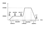
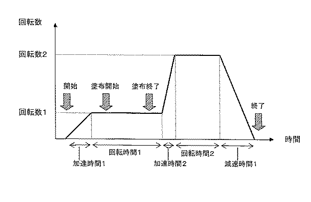
スピンコートプロセスを図1に示した。開始後の2秒の加速時間1内で、基板回転数を0から30rpm(回転数1)まで上昇させた。次に、8秒の回転時間1中の内6秒間に渡り、ノズルから樹脂の吐出を行った。樹脂の吐出位置は基板半径25mmの位置で行ったが、上記回転により基板半径約30mmにまで樹脂が延展した。次に、ノズルをディスク上から十分遠く退避させた後、1秒の加速時間2内で、回転数を回転数1の30rpmから回転数2の2000rpmまで上昇させた。次に、紫外線硬化樹脂の厚さをディスク面上で一様にするため、6秒の回転時間2の間、回転数2を保った。最後に、2秒の減速時間中に回転数を0に下げた(終了)。次に、上記塗布プロセスで樹脂が塗布された基板を紫外線照射装置に移動し、60rpmの回転をさせながら5秒間の紫外線照射を行うことにより、樹脂を硬化させた。 The spin coating process is shown in FIG. The substrate rotation speed was increased from 0 to 30 rpm (rotation speed 1) within an acceleration time 1 of 2 seconds after the start. Next, the resin was discharged from the nozzle over 6 seconds in the rotation time 1 of 8 seconds. The resin was discharged at a position with a substrate radius of 25 mm, but the resin spread to a substrate radius of about 30 mm by the above rotation. Next, after the nozzle was retracted sufficiently far from the disk, the rotation speed was increased from 30 rpm at the rotation speed 1 to 2000 rpm at the rotation speed 2 within the acceleration time 2 of 1 second. Next, in order to make the thickness of the ultraviolet curable resin uniform on the disk surface, the rotation speed 2 was maintained for a rotation time 2 of 6 seconds. Finally, the rotational speed was reduced to 0 during the deceleration time of 2 seconds (end). Next, the substrate coated with the resin in the coating process was moved to an ultraviolet irradiation device, and the resin was cured by performing ultraviolet irradiation for 5 seconds while rotating at 60 rpm.
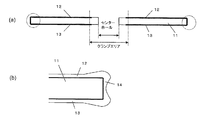
以上のような塗布プロセス及び紫外線硬化プロセスは、ガラス姿勢制御兼光学補正板の両面に対して行った。図2は、上記プロセスの結果得られた姿勢制御兼光学補正板の模式図である。図2(a)は塗布後の断面図、図2(b)は図2(a)に円で囲んで示した外周端面部の断面図である。図示したように、光学ガラス基板11の外周端面部には樹脂の回り込みが発生するため、上面の帯電防止コート12と下面の帯電防止コート13が基板外周端面部の帯電防止コート14を介して繋がった。以上により、帯電防止コート塗布前の表面電気抵抗が1014Ω以上であったのに対し、コート後は1010Ωになった。
The coating process and the ultraviolet curing process as described above were performed on both sides of the glass attitude control and optical correction plate. FIG. 2 is a schematic diagram of the attitude control and optical correction plate obtained as a result of the above process. FIG. 2A is a cross-sectional view after coating, and FIG. 2B is a cross-sectional view of the outer peripheral end face portion surrounded by a circle in FIG. 2A. As shown in the figure, since the resin wraps around the outer peripheral surface of the
ここで、帯電防止コートをクランパーからの力がかかるクランプエリアに形成しなかったのは、クランパーの着脱を繰返すうちにクランプエリアに形成した塗膜が応力を受けて剥がれ、塵埃が発生するのを防止するためである。光学ガラス基板上面(クランパー側)の帯電防止コートがクランパーと接触していなくとも、光学ガラス基板下面に形成された帯電防止コートがスピンドルの光ディスク保持部と接触すれば、結果的に光学ガラス基板の上下面の帯電防止コートがスピンドルの光ディスク保持部を介して接地されることになるため、問題ない。 Here, the antistatic coat was not formed in the clamp area where the force from the clamper was applied. The reason is that the coating film formed on the clamp area peels off due to stress and repeatedly generates dust while the clamper is repeatedly attached and detached. This is to prevent it. Even if the antistatic coating on the upper surface of the optical glass substrate (clamper side) is not in contact with the clamper, if the antistatic coating formed on the lower surface of the optical glass substrate is in contact with the optical disk holding portion of the spindle, the optical glass substrate There is no problem because the antistatic coats on the upper and lower surfaces are grounded via the optical disk holding part of the spindle.
本発明による姿勢制御兼光学補正板の別の実施例について説明する。本実施例では、91mmφ、中心穴径15mmφ、厚さ1.1mmの光学ガラス(BK7)にマグネトロンスパッタ法によって導電性薄膜を形成した。スパッタ方によって形成する導電性薄膜は、塗布によって形成する帯電防止コートと異なり堅牢であるため、クランパーからの力が反復してかかっても剥がれる心配はない。そこで本実施例では、センターホールを含め光学ガラスの全面に導電性薄膜を形成した。 Another embodiment of the posture control and optical correction plate according to the present invention will be described. In this example, a conductive thin film was formed on an optical glass (BK7) having a diameter of 91 mmφ, a center hole diameter of 15 mmφ, and a thickness of 1.1 mm by magnetron sputtering. Since the conductive thin film formed by the sputtering method is robust unlike the antistatic coating formed by coating, there is no fear of peeling even when the force from the clamper is repeatedly applied. Therefore, in this example, a conductive thin film was formed on the entire surface of the optical glass including the center hole.
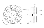
成膜対象となる光学ガラス基板を、スパッタキャリアに8箇所有るパレット上にセットした。図3に示したように、パレット21には永久磁石22が埋め込まれており、磁性SUS430で作製された内周マスク23とパレット−内周マスク間にあるダミー基板24を磁力で保持する。ダミー基板24は、パレット21がスパッタされないようにするために使用した。次に、内周マスク23上に両面テープでガラス基板25を固定した。スパッタキャリアは90rpmで回転し、且つスパッタキャリア上の8個のパレット21は歯車でスパッタキャリアとつながれており、スパッタキャリアの回転と連動して自転するようになっている。スパッタキャリアが一回転するとパレット21が5回転するようにセットした。
The optical glass substrate to be deposited was set on a pallet having eight locations on the sputter carrier. As shown in FIG. 3,
以上のような配置にすると、スパッタ粒子の回り込みが大きく発生するようになり、ガラス基板の外周端、及びセンターホール端にもスパッタ成膜されるようになった。導電性薄膜としては、表1に示すように、Si,Al,APC(Ag−Pd−Cu合金),Pdを種々の膜厚で成膜した。なお、両面テープが粘着した場所はアルコールで洗浄し、ガラス基板の両面に対して成膜を行った。 With the arrangement as described above, spattering of sputtered particles is greatly generated, and sputter film formation is also performed at the outer peripheral edge and the center hole edge of the glass substrate. As the conductive thin film, as shown in Table 1, Si, Al, APC (Ag—Pd—Cu alloy), and Pd were formed in various film thicknesses. The place where the double-sided tape was adhered was washed with alcohol, and film formation was performed on both sides of the glass substrate.
表1に、Si,Al,APC(Ag−Pd−Cu合金),Pd、その多元合金、及び帯電防止コートの表面抵抗と、光学ガラスの透過率を1.0としたときの透過率を示す。Al膜を除く金属薄膜では、帯電防止コートに比べるとその表面抵抗が2桁から3桁良くなるが、一方帯電防止コートと比べると透過率が落ちた。ここでAl膜の表面抵抗が他の金属膜と比較して高いのは、表面に酸化膜ができるためと考えられる。また他の金属膜でも、厚さが1nm以下になると通常のスパッタでは孤立した島状に金属粒子が分布するようになるため、表面抵抗値が急に高くなる(2桁以上高くなる)。このため、帯電防止対策と情報再生強度を両立させるためには、純Alを除く金属薄膜(Ag,Pd,Si及びそれらの合金とAlSi合金)を膜厚1〜5nm形成するか、または帯電防止コートを施すのが適切である。 Table 1 shows the surface resistance of Si, Al, APC (Ag—Pd—Cu alloy), Pd, its multicomponent alloy, and antistatic coating, and the transmittance when the transmittance of the optical glass is 1.0. . In the metal thin film excluding the Al film, the surface resistance is improved by two to three orders of magnitude as compared with the antistatic coat, but the transmittance is lowered as compared with the antistatic coat. Here, it is considered that the surface resistance of the Al film is higher than that of other metal films because an oxide film is formed on the surface. In other metal films, when the thickness is 1 nm or less, metal particles are distributed in an isolated island shape in normal sputtering, so that the surface resistance value is rapidly increased (increased by two orders of magnitude or more). Therefore, in order to achieve both antistatic measures and information reproduction strength, a metal thin film (Ag, Pd, Si and their alloys and AlSi alloy) excluding pure Al is formed to a thickness of 1 to 5 nm, or antistatic. It is appropriate to apply a coat.
こうして作製した本発明の姿勢制御兼光学補正板を市販の光ディスクドライブのスピンドルのディスク保持部に、帯電防止コートあるいは金属薄膜(以下、両者をまとめて導電性コートという)が電気的に連結されるように設置した。 An antistatic coating or a metal thin film (hereinafter collectively referred to as a conductive coating) is electrically connected to the disk holding portion of the spindle of a commercially available optical disk drive with the attitude control and optical correction plate of the present invention thus manufactured. Was installed.
図4は、帯電防止コートを施した姿勢制御兼光学補正板を用いた場合の、光学ガラスへの帯電防止コートの形成状態とスピンドルへの設置状態を示す概略図である。図4(a)は、姿勢制御兼光学補正板の平面図、図4(b)はスピンドルのディスク保持部への設置状態を示す断面模式図である。フレキシブル光ディスク31、帯電防止コート33を施した姿勢制御兼光学補正板32、及びドライブのスピンドル35が電気的に連結されていることを示す。フレキシブル光ディスク31及び姿勢制御兼光学補正板32は、クランパー34によってスピンドル35に固定される。なお、図4(a)には光学ガラスのクランパーエリア外全面に帯電防止コート33を施した姿勢制御兼光学補正板32が示されているが、仮に部分的なコートであっても、フレキシブル光ディスク31、姿勢制御兼光学補正板32、ドライブのスピンドル35が電気的に連結されていれば本発明の効果は得られる。
FIG. 4 is a schematic diagram showing the state of formation of the antistatic coat on the optical glass and the state of installation on the spindle when the posture control and optical correction plate with the antistatic coat is used. FIG. 4A is a plan view of the attitude control and optical correction plate, and FIG. 4B is a schematic cross-sectional view showing a state where the spindle is installed in the disk holding portion. It shows that the flexible
図5は、クランパーの移動機構の一例を示す概略図である。図5(a)は概略斜視図、図5(b)は概略側面図である。クランパー及びスピンドルは十分導電性を有する材質で作製され、同じく十分な導電性の有るドライブ本体と電気的に接続されている。クランパーはドライブ本体の天板に、クランパー自身の回転を妨げないように装着されており、スピンドルは光ディスクがドライブ内に挿入される前には、光ディスクの挿入を妨げないような位置に降りている。光ディスクがドライブ内に挿入される際には、上下動機構によりスピンドルが上昇して光ディスクのセンターホールを受け止め、続いて天板に装着されているクランパーが光ディスクの所定の場所に嵌め合う。上下動機構、クランパー及びピックアップは光ディスクの記録再生が適切に行われる位置に固定される。 FIG. 5 is a schematic diagram illustrating an example of a clamper moving mechanism. FIG. 5A is a schematic perspective view, and FIG. 5B is a schematic side view. The clamper and the spindle are made of a material having sufficient conductivity, and are electrically connected to a drive body having sufficient conductivity. The clamper is mounted on the top plate of the drive body so as not to disturb the rotation of the clamper itself, and the spindle is lowered to a position that does not prevent the optical disk from being inserted before the optical disk is inserted into the drive. . When the optical disk is inserted into the drive, the spindle is raised by the vertical movement mechanism to receive the center hole of the optical disk, and then the clamper mounted on the top plate fits in a predetermined place on the optical disk. The vertical movement mechanism, the clamper, and the pickup are fixed at positions where recording and reproduction of the optical disk are appropriately performed.
このような光ディスクドライブにフレキシブル光ディスクを装填するに当たっては、まず、本発明のフレキシブル基板用姿勢制御兼光学補正板をスピンドルに装填し、その後、姿勢制御兼光学補正板の上にフレキシブル光ディスクを装填する。上記光ディスクのクランピング過程により、帯電防止対策が施されている姿勢制御兼光学補正板とドライブ本体が電気的に接続される。 In loading a flexible optical disk into such an optical disk drive, first, the attitude control / optical correction plate for flexible substrate of the present invention is loaded on the spindle, and then the flexible optical disk is loaded on the attitude control / optical correction plate. . By the clamping process of the optical disk, the attitude control and optical correction plate for which antistatic measures are taken and the drive body are electrically connected.
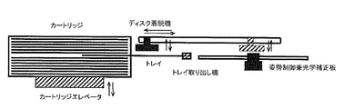
図6は、姿勢制御兼光学補正板上にフレキシブル光ディスクを装填する機構の例を示す図である。この例では、フレキシブル光ディスクを支え保管するトレイを多数収納するカートリッジを用意する。カートリッジは、カートリッジエレベータにより上下して、目的とするフレキシブル光ディスクが保管されているトレイの高さをトレイ取り出し機の高さに合わせる。次に、トレイ取り出し機は、カートリッジから、目的とするフレキシブル光ディスクの入ったトレイを引き出す。引き出されたトレイ上のフレキシブル光ディスクは、ディスク着脱機により吸着して取り出され、姿勢制御兼光学補正板上に運ばれる。その後、ディスク着脱機は、吸着したフレキシブル光ディスクを姿勢制御兼光学補正板上に乗せ、吸着を解除する。こうして、光ディスクドライブのスピンドルに装填された姿勢制御兼光学補正板上にフレキシブル光ディスクが装着される。姿勢制御兼光学補正板上のフレキシブル光ディスクを収納するときは、上記の逆のプロセスによりカートリッジのトレイに収納する。 FIG. 6 is a diagram showing an example of a mechanism for loading a flexible optical disk on the attitude control / optical correction plate. In this example, a cartridge for storing a large number of trays for supporting and storing a flexible optical disk is prepared. The cartridge is moved up and down by a cartridge elevator so that the height of the tray in which the target flexible optical disk is stored matches the height of the tray take-out machine. Next, the tray take-out machine pulls out the tray containing the target flexible optical disk from the cartridge. The flexible optical disk on the pulled-out tray is picked up and taken out by a disk attaching / detaching machine, and is carried onto the attitude control / optical correction plate. Thereafter, the disk attaching / detaching machine places the sucked flexible optical disk on the attitude control / optical correction plate and releases the suction. Thus, the flexible optical disk is mounted on the attitude control and optical correction plate loaded on the spindle of the optical disk drive. When the flexible optical disk on the attitude control / optical correction plate is stored, it is stored in the cartridge tray by the reverse process.
本発明の効果を検証するために、市販の5XMOドライブの外枠を外し、上述したフレキシブル基板用姿勢制御兼光学補正板がむき出しになるようにして、オフィス環境で1週間放置することにより塵埃検査を行った。比較用に導電性コートを施さない光学ガラス基板も用意し、導電性コートを施したものと同条件にして1週間放置した。 In order to verify the effect of the present invention, the outer frame of a commercially available 5XMO drive is removed, and the above-mentioned flexible substrate attitude control and optical correction plate is exposed, and left in the office environment for one week to detect dust. Went. For comparison, an optical glass substrate not provided with a conductive coat was also prepared and left for one week under the same conditions as those for the conductive coat.
まず、姿勢制御兼光学補正板をオフィス環境で放置する前に、フレキシブル光ディスクを、導電性コートを施した姿勢制御兼光学補正板上(条件1とする)と、施さなかったガラス基板上(条件2とする)に載置して読み取り動作を行い、塵埃検査としてのエラーレート測定を行った。初めに10枚のフレキシブル光ディスクを準備し、これらのディスクに対して条件1用のドライブを用いてサーティファイを行い、PDL(プライマリディフェクトリスト)を登録した。これによりスタンパに起因する共通欠陥を取り除くようにした。次に、疑似ランダムデータをライトし、後にリードして、初期状態のエラーレート測定を各ディスクに対して行った。表2は上記過程によって得られた10枚のディスクのPDL数とエラーレートを示した表である。特に問題となるディスクは無く、エラーレートは10−5前半〜10−6後半の値だった。 First, before leaving the attitude control / optical correction plate in an office environment, the flexible optical disk is placed on the attitude control / optical correction plate with the conductive coating (condition 1) and on the glass substrate that has not been applied (conditions). 2), the reading operation was performed, and the error rate was measured as a dust test. First, ten flexible optical discs were prepared, and certification was performed on these discs using a drive for condition 1, and a PDL (primary defect list) was registered. As a result, common defects caused by the stamper were removed. Next, pseudo random data was written and read later, and the error rate in the initial state was measured for each disk. Table 2 shows the number of PDLs and error rates of the 10 discs obtained by the above process. There was no particular problem disk, and the error rate was a value in the first half of 10-5 to the second half of 10-6 .
また、ドライブ間の特性相違を調べるため、これら10枚のディスクからNo.3とNo.9のディスクを用いて条件1、2用のドライブにかけた時のそれぞれのエラーレートを測定した。その結果を示したのが表3である。ドライブ2の方が若干特性は良いものの、塵埃に対するディスク特性を比較する上で特に問題のないことが分かった。 In addition, in order to investigate the difference in characteristics between the drives, no. 3 and No. Each of the error rates was measured when the disk of No. 9 was used and the drive for conditions 1 and 2 was applied. Table 3 shows the results. Although the drive 2 has slightly better characteristics, it has been found that there is no particular problem in comparing the disk characteristics against dust.
次に、フレキシブル光ディスクを姿勢制御兼光学補正板から外して別の専用のカートリッジに保存した。ここで、このカートリッジは十分塵埃に対する対策が取られている。一方、条件1,2の姿勢制御兼光学補正板は、ドライブに設置したまま1週間オフィス環境で放置した。放置後の測定に際しては、用意した10枚のディスクの内適当なもの2枚を選別し、条件1,2の姿勢制御兼光学補正板上に設置した。次にリードオンリーの状態でこれら2枚のディスクのエラー測定を行った。本実施例ではディスクNo.3とNo.9を選び、それぞれ条件1、条件2用のディスクとして用いた。 Next, the flexible optical disk was removed from the attitude control and optical correction plate and stored in another dedicated cartridge. Here, this cartridge has sufficient measures against dust. On the other hand, the posture control and optical correction plate of Conditions 1 and 2 was left in the office environment for one week while being installed in the drive. For the measurement after being left, two appropriate ones of the 10 prepared disks were selected and placed on the attitude control and optical correction plate of conditions 1 and 2. Next, error measurement of these two disks was performed in a read-only state. In this embodiment, the disk No. 3 and No. 9 was selected and used as a disk for conditions 1 and 2 respectively.
測定結果を以下に述べる。まずエラーレートに関しては、表4に示したように、条件1の場合、初期状態での値が2.78×10⁻⁵であったのに対して、塵埃試験後には4.5×10⁻⁵になった。一方、条件2の場合初期状態での値が1.19×10⁻⁵であったのに対して、塵埃試験後には2.00×10⁻³になった。 The measurement results are described below. For the first error rate, as shown in Table 4, under the condition 1, whereas the value in the initial state was 2.78 × 10 -5, after dust test 4.5 × 10 - It became 5 . On the other hand, in the case of condition 2, the value in the initial state was 1.19 × 10 −5 , whereas after the dust test, it was 2.00 × 10 −3 .
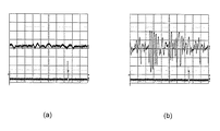
図7に、条件1、2に対してのディスク内周部での和信号(ホトディテクターで受光したディスクからのレーザー反射信号)を示した。図7(a)は条件1のものであり、図7(b)は条件2のものである。条件1に比べ条件2の方に顕著にレベル変動が有り、塵埃または基板の上下変動が多くあることが分かった。 FIG. 7 shows the sum signal (laser reflection signal from the disc received by the photodetector) at the inner periphery of the disc for conditions 1 and 2. 7A shows the condition 1, and FIG. 7B shows the condition 2. It was found that there was a significant level fluctuation in condition 2 compared to condition 1, and there was a lot of vertical fluctuation of dust or the substrate.
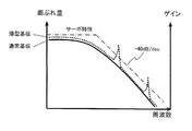
図8は、面ぶれ及びフォーカスサーボの周波数特性を表す図である。
通常、基板が回転しているときのz軸方向の変位(y(t)とする)は、
y(t) = δsinωt (δ;最大変位量、ω;角速度)
と表される。このときのz軸方向の加速度(aとする)は一般に面ぶれ加速度と呼ばれ、
a = y(t)″= -δω2sinωt
と表される。変位δをデシベルで表現すると、
δ = 20log(a/ω2) = -40log(f) -40log(2π) + 20log(a)
と表される(図8中、実線)。
FIG. 8 is a diagram illustrating the frequency characteristics of surface blur and focus servo.
Usually, the displacement in the z-axis direction (y (t)) when the substrate is rotating is:
y (t) = δsinωt (δ: maximum displacement, ω: angular velocity)
It is expressed. In this case, the acceleration in the z-axis direction (assumed as a) is generally called surface acceleration,
a = y (t) ″ = -δω2sinωt
It is expressed. Expressing the displacement δ in decibels,
δ = 20log (a / ω2) = -40log (f) -40log (2π) + 20log (a)
(A solid line in FIG. 8).
ドライブでは、フォーカスサーボにより、上記ディスクの面ぶれ(面ぶれ加速度)に対してアクチュエーター及び対物レンズが余裕を持って追従できるような特性にする(図8中、一点鎖線)。従って、ドライブのフォーカスサーボにより面ぶれ(面ぶれ加速度)が十分低減されるため、正しくレーザービームが情報面にフォーカスされる。 In the drive, the characteristics are set so that the actuator and objective lens can follow the above-mentioned disc surface blur (surface motion acceleration) with a margin by the focus servo (the dashed line in FIG. 8). Accordingly, the surface blur (surface motion acceleration) is sufficiently reduced by the focus servo of the drive, so that the laser beam is correctly focused on the information surface.
ところが基板厚が0.1mm程度のフレキシブル光ディスクでは、姿勢制御兼光学補正板に静電気が蓄積された状態でフレキシブルディスクを載置すると、姿勢制御兼光学補正板とフレキシブル光ディスクの間に、空気が閉じこめられた小さな領域(以後、“エア噛み”という)がいくつも発生する。またこのエア噛みは、スピンドルを回転しても消えずに姿勢制御兼光学補正板とフレキシブル光ディスクの間に残るため、“エア噛み”によって局所的な面ぶれが発生する。従ってこのときの変位量は、
y(t) = δsinωt +(局所的な面ぶれによる高次の変位量)
と表される。即ち、第2項(局所的な面ぶれによる高次の変位量)の時間に対する2回微分による面ぶれ加速度が新たに加わるため(図8中、点線)、ドライブによるフォーカス追従が困難になってくる。以上から、姿勢制御兼光学補正板とフレキシブル光ディスクには上記静電気を起源とする“エア噛み”を対策することが、安定なフォーカシングを行うための重要な課題である。
However, in a flexible optical disk having a substrate thickness of about 0.1 mm, when the flexible disk is placed with static electricity accumulated on the attitude control / optical correction plate, air is trapped between the attitude control / optical correction plate and the flexible optical disk. A number of small areas (hereinafter referred to as “air biting”) occur. Further, this air biting does not disappear even when the spindle is rotated, and remains between the attitude control / optical correction plate and the flexible optical disk, so that local air movement occurs due to “air biting”. Therefore, the amount of displacement at this time is
y (t) = δsinωt + (High-order displacement due to local surface shake)
It is expressed. That is, since the surface blur acceleration due to the second derivative with respect to the time of the second term (high-order displacement due to local surface blur) is newly added (dotted line in FIG. 8), it becomes difficult to follow the focus by the drive. come. From the above, it is an important issue for stable focusing to take measures against “air biting” originating from the static electricity in the attitude control / optical correction plate and the flexible optical disk.
図9に、静止時レーザー変位計で測定した、厚板光ディスク(0.6mm厚)とフレキシブル光ディスク(0.1mm厚、但し姿勢制御兼光学補正板あり)の半径30mmにおける変位量を示す。図から明らかなように、厚板光ディスクの場合、ほぼ正弦波カーブで表現できるのに対して、フレキシブル光ディスクの場合には正弦波カーブの他に別な変位が乗っていることが分かる。また図9から、この変位量は10〜20μm(P−P)で、大きさが約5mm〜10mm(横軸フルスケールがディスク1周に当たり約190mm)であることが分かる。 FIG. 9 shows the amount of displacement of a thick optical disk (0.6 mm thick) and a flexible optical disk (0.1 mm thick, with attitude control and optical correction plate) at a radius of 30 mm, as measured by a stationary laser displacement meter. As can be seen from the figure, in the case of a thick optical disc, it can be expressed by a substantially sinusoidal curve, whereas in the case of a flexible optical disc, it can be seen that there is another displacement in addition to the sinusoidal curve. Further, FIG. 9 shows that the amount of displacement is 10 to 20 μm (PP) and the size is about 5 mm to 10 mm (the horizontal axis full scale is about 190 mm per disk circumference).
ここで姿勢制御兼光学補正板に、本発明のように金属薄膜あるいは帯電防止コートにより静電気対策を行い、これにフレキシブル光ディスクを乗せて変位量測定を行った。測定に際してはステッピングモーター制御によるディスク周方向をスキャンするφステージと、ディスク半径方向をスキャンするX軸ステージを組み合わせることによりディスク全体を測定した。ここでディスク周方向に関しては約0.12°毎に、ディスク半径方向に関しては2mm毎にスキャンした。その結果を表5にまとめた。表5から、静電気対策を施した姿勢制御兼光学補正板を用いることにより、フレキシブル光ディスクの局所面ぶれは、その高さ、数とも小さくなることが分かる。 Here, a countermeasure against static electricity was taken on the attitude control / optical correction plate by using a metal thin film or antistatic coating as in the present invention, and a flexible optical disk was placed on this to measure the displacement. In the measurement, the entire disk was measured by combining a φ stage that scans the circumferential direction of the disk by stepping motor control and an X-axis stage that scans the radial direction of the disk. Here, scanning was performed every about 0.12 ° in the disk circumferential direction and every 2 mm in the disk radial direction. The results are summarized in Table 5. From Table 5, it can be seen that the use of the posture control and optical correction plate with countermeasures against static electricity reduces the local surface blur of the flexible optical disc in both height and number.
ここで、記録再生機のフォーカスエラー信号を調べると、エア噛みは面ぶれとして観察される。この面ぶれ量が記録再生機のフォーカス追従量よりも大きくなると、情報再生信号の劣化が起きたり、場合によってはトラック追従さえ不可能になる。 Here, when the focus error signal of the recording / reproducing apparatus is examined, the air biting is observed as surface blurring. When this surface blur amount becomes larger than the focus follow-up amount of the recording / reproducing device, the information reproduction signal is deteriorated or even the track follow-up becomes impossible in some cases.
一例として、図10に、1.2mm厚の通常のDVDと、100μm厚のフレキシブル光ディスクのフォーカスエラー信号を比較して示す。但し、フレキシブル光ディスクは、帯電防止策を施していない厚さ500μmの光学ガラスに載せて、ドライブのスピンドルに固定した。測定は、半径30mmの位置で線速7m/sで行った。図10(a)は、通常のDVDのフォーカスエラー信号を表し、図10(b)はフレキシブル光ディスクのフォーカスエラー信号を表す。図から明らかなように、フレキシブルディスクのフォーカスエラー信号の方が通常のDVDよりも極めて大きく、エア噛みが大きく発生していることが判る。 As an example, FIG. 10 shows a comparison between focus error signals of a normal DVD having a thickness of 1.2 mm and a flexible optical disc having a thickness of 100 μm. However, the flexible optical disk was mounted on a 500 μm-thick optical glass that had not been subjected to antistatic measures, and was fixed to the spindle of the drive. The measurement was performed at a linear speed of 7 m / s at a radius of 30 mm. FIG. 10A shows a focus error signal for a normal DVD, and FIG. 10B shows a focus error signal for a flexible optical disk. As can be seen from the figure, the focus error signal of the flexible disk is much larger than that of a normal DVD, and the air biting is greatly generated.
これに対して、帯電防止対策を施した本発明の姿勢制御兼光学補正板(厚さ500μm)にフレキシブル光ディスクを載置した場合のフォーカスエラー信号の最大値を、表6にまとめた。帯電防止対策を施した姿勢制御兼光学補正板を使用すると、帯電防止対策を施していない姿勢制御兼光学補正板を使用した場合に比較して、フォーカスエラー信号が小さくなっていることが分かる。これは、帯電防止対策を施すことによってエア噛みの発生が低減したためと考えられる。
On the other hand, Table 6 summarizes the maximum value of the focus error signal when the flexible optical disk is placed on the attitude control and optical correction plate (
以上の結果から、姿勢制御兼光学補正板に導電性コートを施し、且つフレキシブル光ディスク、姿勢制御兼光学補正板、ドライブを電気的に連結することにより、姿勢制御兼光学補正板またはフレキシブル光ディスクに付着する塵埃を効果的に減らすことができ、また姿勢制御兼光学補正板とフレキシブル光ディスクの間に空気が閉じこめられる“エア噛み”の発生を抑制することができることが示された。 Based on the above results, the attitude control / optical correction plate is coated with a conductive coating, and the flexible optical disk, the attitude control / optical correction plate, and the drive are electrically connected to adhere to the attitude control / optical correction plate or flexible optical disk. It has been shown that it is possible to effectively reduce the amount of dust, and to suppress the occurrence of “air biting” in which air is trapped between the attitude control and optical correction plate and the flexible optical disk.
11:光学ガラス基板、12:上面の帯電防止コート、13:下面の帯電防止コート、14:基板外周端面部の帯電防止コート、21:パレット、22:永久磁石、23:内周マスク、24:ダミー基板、25:ガラス基板、31:フレキシブル光ディスク、32:姿勢制御兼光学補正板、33:帯電防止コート、34:クランパー、35:スピンドル 11: Optical glass substrate, 12: Antistatic coating on upper surface, 13: Antistatic coating on lower surface, 14: Antistatic coating on outer peripheral surface of substrate, 21: Pallet, 22: Permanent magnet, 23: Inner peripheral mask, 24: Dummy substrate, 25: Glass substrate, 31: Flexible optical disk, 32: Attitude control and optical correction plate, 33: Antistatic coating, 34: Clamper, 35: Spindle
Claims (6)
前記透明ガラス基板の表面、裏面及び外側面に導電性コートが形成され、光ディスクドライブのスピンドルに固定されたとき、前記透明ガラス基板の表面、裏面及び外側面に形成された導電性コートが前記スピンドルと電気的に接続されることを特徴とするフレキシブル光ディスク用姿勢制御兼光学補正板。 A transparent glass substrate having a flexible optical disk mounting surface and a central opening that fits into the spindle of the optical disk drive. When fixed to the spindle of the optical disk drive, laser light used for recording / reproducing information is passed through the transparent glass substrate. A posture control and optical correction plate for a flexible optical disc that is irradiated onto the flexible optical disc placed on the optical disc placement surface,
When the conductive coating is formed on the front, back and outer surfaces of the transparent glass substrate and fixed to the spindle of the optical disk drive, the conductive coating formed on the front, back and outer surfaces of the transparent glass substrate is the spindle. A posture control and optical correction plate for a flexible optical disc, characterized in that it is electrically connected to the optical disc.
Priority Applications (1)
| Application Number | Priority Date | Filing Date | Title |
|---|---|---|---|
| JP2005115812A JP2006294167A (en) | 2005-04-13 | 2005-04-13 | Posture control and optical correction plate for flexible optical disk |
Applications Claiming Priority (1)
| Application Number | Priority Date | Filing Date | Title |
|---|---|---|---|
| JP2005115812A JP2006294167A (en) | 2005-04-13 | 2005-04-13 | Posture control and optical correction plate for flexible optical disk |
Publications (2)
| Publication Number | Publication Date |
|---|---|
| JP2006294167A true JP2006294167A (en) | 2006-10-26 |
| JP2006294167A5 JP2006294167A5 (en) | 2008-05-08 |
Family
ID=37414561
Family Applications (1)
| Application Number | Title | Priority Date | Filing Date |
|---|---|---|---|
| JP2005115812A Withdrawn JP2006294167A (en) | 2005-04-13 | 2005-04-13 | Posture control and optical correction plate for flexible optical disk |
Country Status (1)
| Country | Link |
|---|---|
| JP (1) | JP2006294167A (en) |
Cited By (2)
| Publication number | Priority date | Publication date | Assignee | Title |
|---|---|---|---|---|
| JP2008287819A (en) * | 2007-05-18 | 2008-11-27 | Hitachi Maxell Ltd | Optical disc body |
| JP2009241372A (en) * | 2008-03-31 | 2009-10-22 | Hitachi High-Technologies Corp | Fine structure transferring machine |
-
2005
- 2005-04-13 JP JP2005115812A patent/JP2006294167A/en not_active Withdrawn
Cited By (2)
| Publication number | Priority date | Publication date | Assignee | Title |
|---|---|---|---|---|
| JP2008287819A (en) * | 2007-05-18 | 2008-11-27 | Hitachi Maxell Ltd | Optical disc body |
| JP2009241372A (en) * | 2008-03-31 | 2009-10-22 | Hitachi High-Technologies Corp | Fine structure transferring machine |
Similar Documents
| Publication | Publication Date | Title |
|---|---|---|
| JP5065461B2 (en) | Optical information recording medium, method for manufacturing the same, and method for holding optical information recording medium | |
| JP3918221B2 (en) | Protective film forming apparatus and protective film forming method | |
| JP2006294167A (en) | Posture control and optical correction plate for flexible optical disk | |
| JP2006059454A (en) | Manufacture apparatus and method of optical recording medium | |
| US5745443A (en) | Magneto-optical disc having a protective film with minimal projections and method of production of same | |
| US20070130578A1 (en) | Thin type optical disk recording and reproducing apparatus and method | |
| EP1756819B1 (en) | Apparatus for attaching and detaching cap for optical disc spin-coating, apparatus for optical disc spin-coating comprising the same, method of manufacturing optical disc using the apparatus for attaching and detaching cap for optical disc spin-coating | |
| JP5485287B2 (en) | Information recording medium manufacturing method and information recording medium | |
| JP4284888B2 (en) | Optical information recording medium | |
| US6941572B2 (en) | Optical information recording medium and optical information recording/reproduction apparatus | |
| JP2008234704A (en) | Turntable for flexible optical disk and method for manufacturing the same, optical information recording / reproducing apparatus, and flexible optical disk rotating apparatus | |
| JP2001023243A (en) | Information recording carrier and information recording carrier reproducing device | |
| JP2007200470A (en) | Information recording / reproducing apparatus and disk clamper | |
| JP4108436B2 (en) | optical disk | |
| JP2008234713A (en) | Manufacturing method of optical recording medium | |
| JP4166630B2 (en) | Optical information recording apparatus and optical information reproducing apparatus | |
| JP4067907B2 (en) | Recording medium having resin substrate | |
| JP5524545B2 (en) | Flexible disk system and method for manufacturing flexible disk | |
| US20050281179A1 (en) | Apparatus for optical disc spin-coating | |
| JP2008027549A (en) | Manufacturing method of optical recording medium | |
| JP2003157574A (en) | Optical disk and optical disk device | |
| JPH0917027A (en) | Optical information recording medium | |
| JP2006164489A (en) | Thin optical disk recording / reproducing apparatus | |
| JP2005310224A (en) | Information recording medium, recording / reproducing apparatus for information recording medium, and identification method for information recording medium | |
| JPH04285738A (en) | Optical information recording medium |
Legal Events
| Date | Code | Title | Description |
|---|---|---|---|
| A521 | Written amendment |
Free format text: JAPANESE INTERMEDIATE CODE: A523 Effective date: 20080319 |
|
| A621 | Written request for application examination |
Free format text: JAPANESE INTERMEDIATE CODE: A621 Effective date: 20080319 |
|
| A761 | Written withdrawal of application |
Free format text: JAPANESE INTERMEDIATE CODE: A761 Effective date: 20090319 |