JP2006295183A - A multi-package module comprising a stacked package comprising a die and a mold body arranged asymmetrically. - Google Patents
A multi-package module comprising a stacked package comprising a die and a mold body arranged asymmetrically. Download PDFInfo
- Publication number
- JP2006295183A JP2006295183A JP2006108295A JP2006108295A JP2006295183A JP 2006295183 A JP2006295183 A JP 2006295183A JP 2006108295 A JP2006108295 A JP 2006108295A JP 2006108295 A JP2006108295 A JP 2006108295A JP 2006295183 A JP2006295183 A JP 2006295183A
- Authority
- JP
- Japan
- Prior art keywords
- package
- die
- substrate
- mounting surface
- semiconductor chip
- Prior art date
- Legal status (The legal status is an assumption and is not a legal conclusion. Google has not performed a legal analysis and makes no representation as to the accuracy of the status listed.)
- Granted
Links
Images






Classifications
-
- H—ELECTRICITY
- H10—SEMICONDUCTOR DEVICES; ELECTRIC SOLID-STATE DEVICES NOT OTHERWISE PROVIDED FOR
- H10W—GENERIC PACKAGES, INTERCONNECTIONS, CONNECTORS OR OTHER CONSTRUCTIONAL DETAILS OF DEVICES COVERED BY CLASS H10
- H10W74/00—Encapsulations, e.g. protective coatings
-
- H—ELECTRICITY
- H10—SEMICONDUCTOR DEVICES; ELECTRIC SOLID-STATE DEVICES NOT OTHERWISE PROVIDED FOR
- H10W—GENERIC PACKAGES, INTERCONNECTIONS, CONNECTORS OR OTHER CONSTRUCTIONAL DETAILS OF DEVICES COVERED BY CLASS H10
- H10W90/00—Package configurations
-
- H—ELECTRICITY
- H10—SEMICONDUCTOR DEVICES; ELECTRIC SOLID-STATE DEVICES NOT OTHERWISE PROVIDED FOR
- H10W—GENERIC PACKAGES, INTERCONNECTIONS, CONNECTORS OR OTHER CONSTRUCTIONAL DETAILS OF DEVICES COVERED BY CLASS H10
- H10W70/00—Package substrates; Interposers; Redistribution layers [RDL]
- H10W70/60—Insulating or insulated package substrates; Interposers; Redistribution layers
-
- H—ELECTRICITY
- H10—SEMICONDUCTOR DEVICES; ELECTRIC SOLID-STATE DEVICES NOT OTHERWISE PROVIDED FOR
- H10W—GENERIC PACKAGES, INTERCONNECTIONS, CONNECTORS OR OTHER CONSTRUCTIONAL DETAILS OF DEVICES COVERED BY CLASS H10
- H10W74/00—Encapsulations, e.g. protective coatings
- H10W74/01—Manufacture or treatment
- H10W74/012—Manufacture or treatment of encapsulations on active surfaces of flip-chip devices, e.g. forming underfills
-
- H—ELECTRICITY
- H10—SEMICONDUCTOR DEVICES; ELECTRIC SOLID-STATE DEVICES NOT OTHERWISE PROVIDED FOR
- H10W—GENERIC PACKAGES, INTERCONNECTIONS, CONNECTORS OR OTHER CONSTRUCTIONAL DETAILS OF DEVICES COVERED BY CLASS H10
- H10W74/00—Encapsulations, e.g. protective coatings
- H10W74/10—Encapsulations, e.g. protective coatings characterised by their shape or disposition
- H10W74/15—Encapsulations, e.g. protective coatings characterised by their shape or disposition on active surfaces of flip-chip devices, e.g. underfills
-
- H—ELECTRICITY
- H10—SEMICONDUCTOR DEVICES; ELECTRIC SOLID-STATE DEVICES NOT OTHERWISE PROVIDED FOR
- H10W—GENERIC PACKAGES, INTERCONNECTIONS, CONNECTORS OR OTHER CONSTRUCTIONAL DETAILS OF DEVICES COVERED BY CLASS H10
- H10W90/00—Package configurations
- H10W90/20—Configurations of stacked chips
- H10W90/291—Configurations of stacked chips characterised by containers, encapsulations, or other housings for the stacked chips
-
- H—ELECTRICITY
- H10—SEMICONDUCTOR DEVICES; ELECTRIC SOLID-STATE DEVICES NOT OTHERWISE PROVIDED FOR
- H10W—GENERIC PACKAGES, INTERCONNECTIONS, CONNECTORS OR OTHER CONSTRUCTIONAL DETAILS OF DEVICES COVERED BY CLASS H10
- H10W90/00—Package configurations
- H10W90/701—Package configurations characterised by the relative positions of pads or connectors relative to package parts
- H10W90/721—Package configurations characterised by the relative positions of pads or connectors relative to package parts of bump connectors
- H10W90/722—Package configurations characterised by the relative positions of pads or connectors relative to package parts of bump connectors between stacked chips
Landscapes
- Wire Bonding (AREA)
- Packaging Frangible Articles (AREA)
- Structures For Mounting Electric Components On Printed Circuit Boards (AREA)
Abstract
【課題】制限を越えてパッケージを可能な限り薄くすることができる半導体チップパッケージを提供する。
【解決手段】半導体チップパッケージは、各基板12に非対称に配置されたダイ14を備える。相補的な配置を備える2つのそのようなパッケージは、2のダイ14が2つの基板12の間のスペースにて並んだ配置となるように、一方が他方に対して逆向きにスタックされる。また、マルチパッケージモジュールは、スタックされたパッケージを備え、それぞれが基板12上で非対称に配置されたダイ14を有する。隣接するスタックされたパッケージは、2のダイ14が2つの基板12の間のスペースにて並んだ配置となるように、スタックに際して一方のパッケージが他方に対して逆向きにされ、ダイ14の相補的且つ非対称な配置を有する。また、製造方法は、パッケージを形成する工程とスタックパッケージモジュールを形成する工程とによって明らかにされる。
【選択図】図1A semiconductor chip package capable of making the package as thin as possible beyond the limits is provided.
A semiconductor chip package includes dies arranged asymmetrically on each substrate. Two such packages with complementary arrangements are stacked one in the opposite direction with respect to the other so that the two dies 14 are arranged side by side in the space between the two substrates 12. The multi-package module also includes stacked packages, each having a die 14 disposed asymmetrically on the substrate 12. Adjacent stacked packages are complementary to one another in stacking so that one package is reversed with respect to the other so that the two dies 14 are arranged side by side in the space between the two substrates 12. And asymmetrical arrangement. The manufacturing method is clarified by a process of forming a package and a process of forming a stack package module.
[Selection] Figure 1
Description
関連した出願とのクロスリファレンスとして、本出願は、2005年4月11日にファイルされた米国仮出願No.60/670,443の利点を主張する。これはその全体を参照することによってここに組み込まれる。 As a cross-reference with related applications, this application claims the benefits of US Provisional Application No. 60 / 670,443 filed April 11, 2005. This is incorporated herein by reference in its entirety.
本発明は、半導体チップパッケージに関し、特に、スタックパッケージモジュールに関する。 The present invention relates to a semiconductor chip package, and more particularly to a stack package module.
半導体チップパッケージにおいて、半導体の機能密度を増大させることに対する一つの手法としては、パッケージ基板にダイを(一方を他方に)スタックするという手法がある。スタックされたダイの電気的な相互接続は、例えばワイヤボンディングによる、ダイとダイ、及び/又は、ダイと基板とで形成されていてもよい。スタックされたダイパッケージにおいて、アセンブリに優先してダイをテストすることは、技術的に難しく、従ってコストがかかる。そして、供給においては、複数の「悪い」ダイが予期される。スタックされたダイパッケージの1つの悪いダイは、パッケージ全体を悪くする可能性があり、それに応じて、特により多くのダイがパッケージにスタックされる場合、スタックされたダイパッケージの製造において、素材の大幅な浪費と製造時間とが必然的に結果として生じ得る。4、5、又は6つものダイを有するスタックされたダイパッケージが使用されている。隣接したダイの間のスペーサーが必要とされている場合でさえ、スタックされたダイパッケージは、非常に薄く形成されることがある。 In a semiconductor chip package, one method for increasing the functional density of a semiconductor is to stack dies (one on the other) on a package substrate. The electrical interconnection of the stacked dies may be formed between the die and the die and / or the die and the substrate, for example by wire bonding. In stacked die packages, testing a die prior to assembly is technically difficult and therefore costly. And in supply, multiple “bad” dies are expected. One bad die of a stacked die package can degrade the entire package, and accordingly, in manufacturing a stacked die package, especially if more dies are stacked in the package, Significant waste and production time can inevitably result. Stacked die packages with as many as 4, 5, or 6 dies are used. Even when spacers between adjacent dies are required, stacked die packages can be made very thin.
半導体チップパッケージにおいて、半導体の機能密度を増大させることに対する別の手法としては、スタックパッケージモジュールを形成するためにパッケージ(一方を他方に)をスタックする手法がある。モジュールの各パッケージは、基板に取り付けられて電気的に相互接続された少なくとも1つのダイを含む。スタックする際のパッケージは、例えばワイヤボンドによってそれぞれのパッケージ基板のボンドサイト間で電気的に相互接続される。これには、パッケージがスタックにて組み立てられる前に完全にテストされ得るという利点がある。即ち、「悪い」パッケージは処分され、「よい」とテストしているパッケージだけがモジュールにて使われる。 As another method for increasing the functional density of a semiconductor in a semiconductor chip package, there is a method of stacking packages (one on the other) to form a stack package module. Each package of the module includes at least one die attached to the substrate and electrically interconnected. The packages for stacking are electrically interconnected between bond sites of the respective package substrates, for example by wire bonds. This has the advantage that the package can be fully tested before being assembled in a stack. That is, “bad” packages are discarded, and only packages that are tested “good” are used in the module.
いくつかの要素は、典型的なスタックパッケージモジュールの厚さに寄与している。最小でも、それぞれの基板とダイとダイ取付接着剤との厚さが関係している。更に、各パッケージのダイがモールドされる(又は、カプセル化される)場合には、一般に、モールドキャップは、ダイの厚さよりも大きい厚さを有し、ダイが基板にワイヤボンドされている場合には、モールドキャップは、ワイヤに加えてワイヤループの高さのバリエーションの差を完全にカバーするために、十分厚くなければならない。そして、一般に、パッケージスタックもまた、モジュールモールド体によってモールドされる又はカプセル化される。それは、更に厚さを追加する。 Several factors contribute to the thickness of a typical stack package module. At a minimum, the thickness of each substrate, die, and die attach adhesive is related. Further, when each package die is molded (or encapsulated), the mold cap generally has a thickness greater than the die thickness, and the die is wire bonded to the substrate. In addition, the mold cap must be thick enough to completely cover the difference in wire loop height variation in addition to the wire. In general, the package stack is also molded or encapsulated by a module mold body. It adds more thickness.
例えば、携帯電話、PDA、デジタルカメラ、及び様々な消費者電子機器などのモバイル機器のように、パッケージ面積とパッケージ厚さとの両方に制限が課される製品において、パッケージ(又はモジュール)を制限を越えて面積を増大させることなく可能な限り薄くすることが望ましい。 For example, mobile devices such as mobile phones, PDAs, digital cameras, and various consumer electronics devices that limit the package (or module) in products that have restrictions on both package area and thickness. It is desirable to make it as thin as possible without increasing the area beyond.
1つの一般的な形態において、本発明は非対称に配置されたダイを備える半導体チップパッケージを特徴とする。相補的な配置を有する2つのそのようなパッケージは、2つのダイが2つの基板の間のスペースに並んだ配置となるように、一方が他方に対して逆向きにスタックされる。ある形態においては、ダイは、接着剤を使ってそれぞれの基板に貼り付けられ、そして、ワイヤボンディングによって基板と電気的に相互接続される。そして、ある形態においては、ダイは、それぞれの基板の上にフリップチップ相互接続によって設置される。ダイは、モールドされてもよい。 In one general form, the invention features a semiconductor chip package with asymmetrically placed dies. Two such packages with complementary arrangements are stacked one side up against the other so that the two dies are arranged side by side in the space between the two substrates. In one form, the dies are affixed to their respective substrates using an adhesive and are electrically interconnected with the substrates by wire bonding. And in one form, the dies are placed on each substrate by flip chip interconnection. The die may be molded.
他の形態において、本発明は、それぞれが非対称にダイを配置して、スタックされたパッケージを有するマルチパッケージモジュールを特徴とする。パッケージは、2つのダイが2つの基板の間のスペースに並んだ配置となるように、スタックに際して一方のパッケージが他方のパッケージに対して逆向きにされて相補的且つ非対称な配置となる。隣接したパッケージ間のZ相互接続は、はんだボールによって成され、そして、はんだボールの高さは、ダイのためのスペースを形成するのに十分なものとなっている。ダイは並べて配置されているので、モジュールの厚さは低減される。 In another form, the invention features multi-package modules having stacked packages, each with asymmetric die placement. The packages are arranged in a complementary and asymmetrical arrangement, with one package turned upside down with respect to the other package during stacking so that the two dies are arranged in the space between the two substrates. The Z interconnection between adjacent packages is made by solder balls, and the height of the solder balls is sufficient to form a space for the die. Since the dies are arranged side by side, the thickness of the module is reduced.
他の形態において、本発明は、パッケージの製造方法とスタックパッケージモジュールの製造方法とを特徴とする。 In another aspect, the invention features a package manufacturing method and a stacked package module manufacturing method.
本発明にかかるスタック可能な相補的なパッケージは、現在入手可能な製造機器と素材と従来の表面実装技術とを用いて製造される。組立工程は、一方が他方の上にスタックされたパッケージを備えるモジュールについての組立工程よりも複雑でないようにすることができ、結果的な厚さプロフィールは、より小さくすることができる。本発明によれば、2つの結合された相補的なパッケージの2つのダイが基板と追加のダイとの間のスペースを占有することと、ダイ取付けとモールドキャップとの厚さが抑制されることという事実の効果によって、モジュールアセンブリにおけるスタックの厚さは低減される。本発明によれば、スタックされた相補的なパッケージの位置合わせの後に、アセンブリ全体に対して1つのはんだボールリフローだけを実行することによって、製造コストは低減される。個々のパッケージは完全に検証可能である。 The stackable complementary package according to the present invention is manufactured using currently available manufacturing equipment and materials and conventional surface mount technology. The assembly process can be less complex than the assembly process for a module with a package stacked one on top of the other, and the resulting thickness profile can be smaller. According to the present invention, two dies in two coupled complementary packages occupy the space between the substrate and the additional die, and the die attachment and mold cap thicknesses are suppressed. The effect of the fact is that the stack thickness in the module assembly is reduced. In accordance with the present invention, manufacturing costs are reduced by performing only one solder ball reflow on the entire assembly after alignment of the stacked complementary packages. Individual packages are fully verifiable.
本発明にかかる半導体チップパッケージは、ダイ実装面とランド面とを有する基板を備えてなり、ダイ実装面はダイ取付領域と空領域とを備え、ダイは、基板のダイ実装面のダイ取付領域に取り付けられることを特徴とする。 A semiconductor chip package according to the present invention includes a substrate having a die mounting surface and a land surface, the die mounting surface includes a die mounting region and an empty region, and the die is a die mounting region on the die mounting surface of the substrate. It is attached to.
また、請求項1に記載の半導体チップパッケージにおいて、ダイは、ダイのアクティブ面を基板に対して外側に向くように方向付けられて接着剤を用いてダイ取付領域に貼り付けられ、ダイのアクティブ面のダイパッドと基板のボンドパッドとの間でワイヤによって電気的に接続されていることが好ましい。 Further, in the semiconductor chip package according to claim 1, the die is oriented so that an active surface of the die faces outward with respect to the substrate, and is attached to the die attachment region using an adhesive, and the active die Preferably, a wire is electrically connected between the die pad on the surface and the bond pad on the substrate.
更に、請求項2に記載の半導体チップパッケージにおいて、モールド体は、ワイヤと少なくともダイのアクティブ面のダイパッドとを囲むことが好ましい。 Furthermore, in the semiconductor chip package according to claim 2, the mold body preferably surrounds the wire and at least the die pad on the active surface of the die.
また、請求項1に記載の半導体チップパッケージにおいて、ダイは、基板に面するアクティブ面で貼り付けられ、ダイのアクティブ面のダイパッドと基板の相互接続サイトとの間でフリップチップ相互接続によってダイ取付領域と電気的に接続されることが好ましい。 2. The semiconductor chip package of claim 1, wherein the die is affixed with an active surface facing the substrate, and the die is attached by flip chip interconnection between the die pad on the active surface of the die and the interconnect site of the substrate. It is preferably electrically connected to the region.
更に、請求項4に記載の半導体チップパッケージにおいて、ダイのアクティブ面と基板のダイ取付領域との間にアンダーフィルを備えることが好ましい。 Furthermore, in the semiconductor chip package according to claim 4, it is preferable that an underfill is provided between the active surface of the die and the die attachment region of the substrate.
また、請求項1に記載の半導体チップパッケージにおいて、基板のダイ実装面上のボールパッドにマウントされるZ相互接続はんだボールを更に備えることが好ましい。 The semiconductor chip package according to claim 1, further comprising a Z interconnection solder ball mounted on a ball pad on a die mounting surface of the substrate.
更に、請求項1に記載の半導体チップパッケージにおいて、基板のランド面上のボールパッドにマウントされるZ相互接続はんだボールを備えることが好ましい。 The semiconductor chip package according to claim 1, further comprising Z interconnect solder balls mounted on ball pads on the land surface of the substrate.
また、本発明にかかる相補的なパッケージペアユニットは、
ダイ実装面とランド面とを具備し、ダイ実装面がダイ取付領域と空領域とを有する第1基板と、
第1基板のダイ実装面のダイ取付領域にダイが取付けられた第1パッケージと、
第1基板のダイ実装面上のボールパッドにマウントされた第1Z相互接続はんだボールと、
を具備する第1半導体チップパッケージと;
ダイ実装面とランド面とを具備し、ダイ実装面がダイ取付領域と空領域とを有する第2基板と、
第1基板のダイ実装面のダイ取付領域にダイが取付けられた第2パッケージと、
を具備する第2半導体チップパッケージとを備え;
第1パッケージは、第1パッケージのダイ実装面が第2パッケージのダイ実装面に面するように第2パッケージにスタックされ、第1パッケージのダイ取付領域は、第2パッケージの空領域と位置合わせされ、第1パッケージの第1Z相互接続はんだボールは、第2基板のダイ実装面上のボールパッドに接触するように構成されていることを特徴とする。
Also, the complementary package pair unit according to the present invention is:
A first substrate having a die mounting surface and a land surface, the die mounting surface having a die attachment region and an empty region;
A first package in which a die is attached to a die attachment region of the die mounting surface of the first substrate;
A first Z interconnect solder ball mounted on a ball pad on the die mounting surface of the first substrate;
A first semiconductor chip package comprising:
A second substrate having a die mounting surface and a land surface, the die mounting surface having a die attachment region and an empty region;
A second package in which a die is attached to the die attachment region of the die mounting surface of the first substrate;
A second semiconductor chip package comprising:
The first package is stacked on the second package so that the die mounting surface of the first package faces the die mounting surface of the second package, and the die mounting area of the first package is aligned with the empty area of the second package The first Z solder balls of the first package are configured to contact the ball pads on the die mounting surface of the second substrate.
また、請求項8に記載の相補的なパッケージペアユニットにおいて、Z相互接続はんだボールは、第1基板のダイ実装面上のボールパッドと第2基板のダイ実装面上の接触ボールパッドとの間のZレベル相互接続を形成するためにリフローされることが好ましい。 9. The complementary package pair unit according to claim 8, wherein the Z interconnection solder ball is between the ball pad on the die mounting surface of the first substrate and the contact ball pad on the die mounting surface of the second substrate. Are preferably reflowed to form a Z-level interconnect.
更に、請求項9に記載の相補的なパッケージペアユニットにおいて、第2基板のランド面上のボールパッドにマウントされた第2Z相互接続はんだボールを備えることが好ましい。 Furthermore, the complementary package pair unit according to claim 9 preferably comprises a second Z interconnect solder ball mounted on a ball pad on a land surface of the second substrate.
また、マルチパッケージモジュールは、請求項9に記載の相補的なパッケージペアユニットと第1及び第2パッケージの間のボリュームにおけるモジュールカプセル体とを備えることを特徴とする。 The multi-package module includes the complementary package pair unit according to claim 9 and a module capsule body in a volume between the first and second packages.
また、マルチパッケージモジュールは、
請求項10記載の第1の相補的なパッケージペアユニットと;
ダイ実装面とランド面とを具備し、ダイ実装面がダイ取付領域と空領域とを有する第3基板と、
第1基板のダイ実装面のダイ取付領域にダイが取付けられた第3パッケージと、
第1基板のダイ実装面上のボールパッドにマウントされた第3Z相互接続はんだボールと;
を具備する第3半導体チップパッケージと、
ダイ実装面とランド面とを具備し、ダイ実装面がダイ取付領域と空領域とを有する第4基板と、
第1基板のダイ実装面のダイ取付領域にダイが取付けられた第4パッケージと、
を具備する第4半導体チップパッケージと;
を有する第2の相補的なパッケージペアユニットとを備え:
第3パッケージは、第3パッケージのダイ実装面が第4パッケージのダイ実装面に面するように第4パッケージにスタックされ、第3パッケージのダイ取付領域は、第4パッケージの空領域と位置合わせされ、第3パッケージの第3Z相互接続はんだボールは、第4基板のダイ実装面上のボールパッドに接触し、更に、第1の相補的なパッケージペアユニットは、第2の相補的なパッケージペアユニットにスタックされ、第2パッケージの第2Z相互接続はんだボールは、第3パッケージ基板のランド面上のボールパッドに接触するように構成されていることを特徴とする。
Multi-package modules
A first complementary package pair unit according to claim 10;
A third substrate having a die mounting surface and a land surface, the die mounting surface having a die mounting region and an empty region;
A third package in which a die is attached to the die attachment region of the die mounting surface of the first substrate;
A third Z interconnect solder ball mounted on a ball pad on the die mounting surface of the first substrate;
A third semiconductor chip package comprising:
A fourth substrate having a die mounting surface and a land surface, the die mounting surface having a die attachment region and an empty region;
A fourth package in which the die is attached to the die attachment region of the die mounting surface of the first substrate;
A fourth semiconductor chip package comprising:
With a second complementary package pair unit having:
The third package is stacked on the fourth package such that the die mounting surface of the third package faces the die mounting surface of the fourth package, and the die mounting area of the third package is aligned with the empty area of the fourth package The third Z interconnect solder balls of the third package are in contact with the ball pads on the die mounting surface of the fourth substrate, and the first complementary package pair unit is the second complementary package pair. The second Z interconnect solder balls of the second package stacked in the unit are configured to contact the ball pads on the land surface of the third package substrate.
また、請求項12に記載のマルチパッケージモジュールにおいて、第1及び第2パッケージの間のボリュームにおけるモジュールカプセル体を更に備えることが好ましい。
The multi-package module according to
更に、請求項13に記載のマルチパッケージモジュールにおいて、第3及び第4パッケージの間のボリュームにおけるモジュールカプセル体を備えることが好ましい。
Furthermore, in the multi-package module according to
更に、請求項14に記載のマルチパッケージモジュールにおいて、第2及び第3パッケージの間のボリュームにおけるモジュールカプセル体を備えることが好ましい。 Furthermore, it is preferable that the multi-package module according to claim 14 further includes a module capsule body in a volume between the second and third packages.
また、本発明にかかる半導体チップパッケージの製造方法は、
第1及び第2面を備え、第1面に第1の模様付けられた金属層を備え第2面に第2の模様付けられた金属層を備えるパッケージ基板を形成するパッケージ基板形成工程と、
ダイのアクティブ面上にダイパッドを備える半導体ダイを形成するダイ形成工程と、
基板の第1面のダイ取付領域にダイをマウントするダイ実装工程と第1の模様付けられた金属層ボンドパッドにダイを電気的に相互接続する相互接続工程と、
を備えることを特徴とする。
In addition, a method for manufacturing a semiconductor chip package according to the present invention includes:
A package substrate forming step comprising: forming a package substrate comprising a first patterned metal layer on the first surface, the package substrate comprising a first patterned metal layer on the first surface, and a second patterned metal layer on the second surface;
Forming a semiconductor die having a die pad on the active surface of the die; and
A die mounting step of mounting the die on the die attachment region of the first surface of the substrate and an interconnection step of electrically interconnecting the die to the first patterned metal layer bond pad;
It is characterized by providing.
また、請求項16記載の半導体チップパッケージの製造方法において、ダイ実装工程は、基板に対して外側を向いているダイのアクティブ面にてダイ取付領域にダイを貼り付けるダイ貼付工程を備え、相互接続工程は、ボンドパッドにてダイパッドのワイヤボンド相互接続を形成するワイヤボンド相互接続形成工程を備えることが好ましい。
17. The method of manufacturing a semiconductor chip package according to
更に、請求項16記載の半導体チップパッケージの製造方法において、ダイ実装工程と相互接続工程とは、基板に対して外側を向いているダイのアクティブ面にてダイ取付領域にダイを位置決めするダイ位置決め工程と、ボンドパッドにてダイパッドのフリップチップ相互接続を形成するフリップチップ相互接続工程とを備えることが好ましい。
17. The method of manufacturing a semiconductor chip package according to
更に、請求項17記載の半導体チップパッケージの製造方法において、ダイとワイヤボンドとをカプセル化するカプセル化工程を備えることが好ましい。
Furthermore, in the method for manufacturing a semiconductor chip package according to
更に、請求項18記載の半導体チップパッケージの製造方法において、ダイと基板との間にアンダーフィルを形成するアンダーフィル形成工程を備えることが好ましい。 Furthermore, in the method for manufacturing a semiconductor chip package according to claim 18, it is preferable to include an underfill forming step of forming an underfill between the die and the substrate.
また、マルチパッケージモジュールの製造方法は、
請求項1に記載の第1及び第2半導体チップパッケージを形成する第1及び第2半導体チップパッケージ形成工程と;
第1パッケージ基板の第1面上のボールパッドに第1Z相互接続はんだボールをマウントするはんだボール実装工程と;
各パッケージ基板の第1面が他のパッケージ基板の第1面に面し、各パッケージ基板のダイ取付領域が他のパッケージ基板の空領域に一致するように、第1及び第2パッケージを互いに関連付けて位置合わせする位置合わせ工程と;
第2パッケージ基板の第1面上のボールパッドにて第1Z相互接続はんだボールが接触するはんだボール接触工程と;
第2パッケージ基板の第1面上のボールパッドと電気的な接続関係をもたらすために第1Z相互接続はんだボールをリフローするリフロー工程と、
を備えることを特徴とする。
In addition, the manufacturing method of the multi-package module is:
A first and second semiconductor chip package forming step of forming the first and second semiconductor chip packages according to claim 1;
A solder ball mounting step of mounting a first Z interconnect solder ball on a ball pad on the first surface of the first package substrate;
Associate the first and second packages with each other so that the first surface of each package substrate faces the first surface of the other package substrate and the die mounting area of each package substrate coincides with the empty area of the other package substrate An alignment step of aligning and
A solder ball contact process in which the first Z interconnect solder balls contact at a ball pad on the first surface of the second package substrate;
A reflow process for reflowing the first Z interconnect solder balls to provide an electrical connection with the ball pads on the first surface of the second package substrate;
It is characterized by providing.
また、請求項21に記載のマルチパッケージモジュールの製造方法において、パッケージ間のモジュールカプセル体を形成する工程を備えることが好ましい。 Furthermore, in the method for manufacturing a multi-package module according to claim 21, it is preferable to include a step of forming a module capsule body between packages.
更に、請求項21に記載のマルチパッケージモジュールの製造方法において、第2パッケージ基板の第2面に第2Z相互接続はんだボールをマウントする工程を備えることが好ましい。 Furthermore, in the method of manufacturing a multi-package module according to claim 21, it is preferable to include a step of mounting a second Z interconnect solder ball on the second surface of the second package substrate.
また、マルチパッケージモジュールの製造方法は、
請求項1に記載の第1及び第2パッケージを形成する第1及び第2パッケージ形成工程と;
第1パッケージ基板の第1面上のボールパッドに第1Z相互接続はんだボールをマウントするはんだボール実装工程と;
互いに面するパッケージのダイ実装面と他方のパッケージ基板の空領域に位置合わせされた各パッケージのダイ取付領域とによって、第2パッケージの上に第1パッケージをスタックする第1パッケージスタック工程と;
第2パッケージ基板の第1面上のボールパッドと電気的な接続関係をもたらすために第1Z相互接続はんだボールをリフローするリフロー工程と、
を備えることを特徴とする。
In addition, the manufacturing method of the multi-package module is:
First and second package forming steps for forming the first and second packages according to claim 1;
A solder ball mounting step of mounting a first Z interconnect solder ball on a ball pad on the first surface of the first package substrate;
A first package stacking step of stacking the first package on the second package by means of a die mounting surface of the package facing each other and a die attachment region of each package aligned with an empty region of the other package substrate;
A reflow process for reflowing the first Z interconnect solder balls to provide an electrical connection with the ball pads on the first surface of the second package substrate;
It is characterized by providing.
更に、請求項24に記載のマルチパッケージモジュールの製造方法において、パッケージ間のモジュールカプセル体を形成する工程を備えることが好ましい。 Furthermore, it is preferable that the method for manufacturing a multi-package module according to claim 24 further includes a step of forming a module capsule body between packages.
また、請求項24に記載のマルチパッケージモジュールの製造方法において、第2パッケージ基板の第2面に第2Z相互接続はんだボールをマウントする工程を備えることが好ましい。
The method of manufacturing a multi-package module according to
また、電子機器は、請求項12に記載のマルチパッケージモジュールを備え、電子機器の基礎的な電気回路と電気的に接続されていることを特徴とする。
An electronic apparatus includes the multi-package module according to
本発明は、図面を参照することによって、さらに詳しく説明される。各図面は本発明の択一的な形態を示している。各図面は、本発明の特徴と他の特徴及び構成との関係を示す概略図であり、一定の比率ではない。説明を明瞭にするため、本発明の形態を示す各図面において、他の図面で示される要素に対応する要素は、すべて容易に同一視できるが、すべてについて特に同じ番号を付しているわけではない。また、本発明についての理解に必要でない箇所において、説明を明瞭にするためにある特徴が示されていない場合にも同様である。例えば、基板表面に模様付けされた金属層は示されず、そして基板へのダイの相互接続(ワイヤまたはバンプ)は示されない。 The invention is explained in more detail by reference to the drawings. Each drawing shows an alternative form of the invention. Each drawing is a schematic diagram showing the relationship between the features of the present invention and other features and configurations, and is not in a fixed ratio. For clarity of explanation, in each drawing showing the embodiment of the present invention, all the elements corresponding to the elements shown in the other drawings can be easily identified, but they are not particularly given the same numbers. Absent. The same applies to the case where certain features are not shown for the sake of clarity in the portions not necessary for understanding the present invention. For example, a patterned metal layer on the substrate surface is not shown, and die interconnections (wires or bumps) to the substrate are not shown.
本発明の1形態によると、パッケージは、基板に非対称に配置されたダイを備える。即ち、ダイは、ダイ取付領域の基板のエッジの方に、基板の反対側のエッジ付近に空領域を残すようにして取り付けられる(取り付けられてワイヤーボンドされる、或いは、フリップチップ方式でマウントされるかの何れかにて取り付けられる)。第1の形態において、相互接続はんだボールは、基板のダイ実装面にマウントされる;そして、相補的な第2の形態において、はんだボールは、基板のダイ実装面の反対側にマウントされる。パッケージの相補的なペアは一方が他方に対して逆向きとなるようにスタックされ、それぞれのパッケージ基板は、その基板のダイ実装面にはんだボールを備えるパッケージのはんだボールによって電気的に相互接続される。はんだボールの高さは、ダイ(そしてダイ取り付け)の厚さを適合させる基板間のスタンドオフを得るために十分に高く、そして、第1パッケージのダイが第2パッケージ基板の空領域のパッケージ基板間のスペースに配置されるように、パッケージは方向付けられる。 According to one form of the invention, the package comprises a die disposed asymmetrically on the substrate. That is, the die is attached to the edge of the substrate in the die attachment area, leaving an empty area near the opposite edge of the substrate (attached and wire-bonded or mounted in a flip chip manner). It is attached by either). In the first configuration, the interconnect solder balls are mounted on the die mounting surface of the substrate; and in a complementary second configuration, the solder balls are mounted on the opposite side of the die mounting surface of the substrate. Complementary pairs of packages are stacked so that one is opposite to the other, and each package substrate is electrically interconnected by the solder balls of the package with solder balls on the die mounting surface of the substrate The The height of the solder balls is high enough to obtain a standoff between the boards that adapts the die (and die attach) thickness, and the first package die is an empty package substrate in the second package substrate. The package is oriented so that it is placed in the space between.
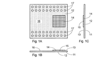
図1(A)、(B)、及び(C)には、本発明にかかる基板12のダイ実装面13上のダイ取付領域15に非対称にマウントされたダイ14が示されている。ダイ取付領域15は、基板のエッジの方に設けられ、基板の反対側のエッジの方に設けられたダイ実装面13の空領域16を残している。パッケージ基板12は、好ましくは、誘電層の間に少なくとも2つの模様付けられた金属層を有するラミネート基板である。即ち、好ましいラミネート基板は、少なくとも、ダイ実装面13に第1「upper」模様付け金属層を、ダイ実装面の反対側の面11(「ランド」面)に第2「lower」模様付け金属層を具備する。種々の金属層は、適切なトレース回路を形成するために模様付けられ、そして、誘電層を通るビアは、層間の接続を果たす。上下の模様付け金属層上の保護層は、ダイの電気接続のためのトレース上のサイトを露出し、はんだボールをマウントするためのボールパッド(ダイ実装面で列又は配列の17にて示される)を露出している開口によって模様付けられている。ダイは、基板に対して外側を向いているダイのアクティブ面にてダイ取付接着剤(ダイ取付エポキシ樹脂やフィルムなど)を用いたダイ取付領域に取り付けられ、そして、基板のダイパッド(図示しない)とボンドパッド(図示しない)との間のワイヤボンドによって電気的に相互接続されてもよい。或いは、ダイは、基板に面しているダイのアクティブ面にてフリップチップアタッチメント(図示しない)によって基板の上にマウントされ、導電性バンプ又はボールを用いた基板のボンドサイトに電気的に相互接続されてもよい。
1A, 1B and 1C show a die 14 mounted asymmetrically on a
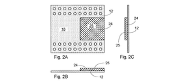
その場合、ダイは、図2(A)、(B)、 及び(C)に示すようにモールドされる。ダイがワイヤボンディングによって相互接続される場合、その後のステップ間でのワイヤへのダメージを防止するために、モールド体を必要としてもよい。モールド体24は、ダイとワイヤボンド(ワイヤボンド相互接続が用いられる場合)とを覆い、そして、実質的に平坦な「upper」表面25を備えるために成形される。ダイがフリップチップ相互接続によって設置される場合には、ダイと基板との間のバンプスタンドオフスペースを満たすと共に相互接続を機械的に安定させるため、アンダーフィルが望ましいが、モールド体は必要としなくてもよい。
In that case, the die is molded as shown in FIGS. 2 (A), (B), and (C). If the dies are interconnected by wire bonding, a mold body may be required to prevent damage to the wire between subsequent steps.
その場合、図3(A)、(B)、及び(C)に示すように、Z相互接続はんだボール37は、基板12のダイ実装面13上のボールパッドにマウントされる。図に示す以外のボールパッドとはんだボールとの配置は、例えば、基板のダイ実装面13の空領域16を閉ざさないような配置であれば何れの配置であっても採用できる。そして、ボールパッドとはんだボールとは、それらが相補的なパッケージに対し第1のパッケージに逆向きにマウントされるよう安定した支持をもたらすように配置される。相補的なパッケージが結合されてはんだボールがリフローした場合には、ダイ(そして、この場合はモールド体)を適合させるためボール高さが隣接した基板の間のクリアランスとなるように、はんだボールは設定される。はんだボールをマウントすると、第1のパッケージ30が完成し、その状態で、はんだボールは基板のダイ実装面にマウントされる。高く評価されるべきことは、はんだボールが2つの相補的なパッケージを結合するためにリフローの間に崩れた場合であっても、モールド体24の上面25は、更なるはんだボールの崩れを抑制して相補的なパッケージ基板の空領域に接触していることである。
In that case, as shown in FIGS. 3 (A), (B), and (C), the Z
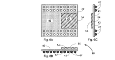
はんだボールが基板のランド面にマウントされる本発明の形態にかかる相補的なパッケージ60は、図4(A)乃至図6(C)に示すように製造することができる。
The
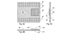
図4(A)、(B)、及び(C)には、本発明にかかる基板42のダイ実装面43上のダイ取付領域45に非対称にマウントされたダイ44が示されている。ダイ取付領域45は、基板のエッジの方に設けられ、基板の反対側のエッジに設けられたダイ実装面43の空領域46を残している。パッケージ基板42は、好ましくは、誘電層の間に少なくとも2つの模様付けられた金属層を有するラミネート基板である。即ち、好ましいラミネート基板は、少なくとも、ダイ実装面43の第1「upper」模様付け金属層とダイ実装面の反対側の面41(「ランド」面)の第2「lower」模様付け金属層とを含む。種々の金属層は、適切なトレース回路を形成するために模様付けられ、そして、誘電層を通るビアは、層間の接続を果たす。上下の模様付け金属層上の保護層は、ダイの電気接続のためのトレース上のサイトを露出し、はんだボールをマウントするためのボールパッド(ダイ実装面で列又は配列の47にて示される)を露出している開口によって模様付けられている。ダイは、基板に対し外側を向いているダイのアクティブ面にてダイ取付接着剤(ダイ取付エポキシ樹脂やフィルムなど)を用いているダイ取付領域に取り付けられ、そして、基板のダイパッド(図示しない)とボンドパッド(図示しない)との間のワイヤボンドによって電気的に相互接続されてもよい。或いは、ダイは、基板に面しているダイのアクティブ面にてフリップチップアタッチメント(図示しない)によって基板の上にマウントされ、導電性バンプ又はボールを用いた基板のボンドサイトに電気的に相互接続されてもよい。
4A, 4B, and 4C show a die 44 mounted asymmetrically on a
その場合、ダイは、図5(A)、(B)、 及び(C)に示すようにモールドされる。ダイがワイヤボンディングによって相互接続される場合、その後のステップ間でのワイヤへのダメージを防止するために、モールド体を必要としてもよい。モールド体54は、ダイとワイヤボンド(ワイヤボンド相互接続が用いられる場合)とを覆い、そして、実質的に平坦な「upper」表面55を備えるために成形される。ダイがフリップチップ相互接続によって設置される場合には、ダイと基板との間のバンプスタンドオフスペースを満たすと共に相互接続を機械的に安定させるため、アンダーフィルが望ましいが、モールド体は必要としなくてもよい。
In that case, the die is molded as shown in FIGS. 5 (A), (B), and (C). If the dies are interconnected by wire bonding, a mold body may be required to prevent damage to the wire between subsequent steps.
その場合、図6(A)、(B)、及び(C)に示すように、Z相互接続はんだボール67は、基板42のランド面41上のボールパッドにマウントされる。図に示す以外のボールパッドとはんだボールとの配置は、以下で説明するように、例えば、マザーボード上、又は追加のアセンブリ上、又は別のサポート上へのアセンブリのマウントに対して安定した支持を供給するような配置であれば何れの配置であっても採用できる。はんだボールをマウントすると、第2パッケージ60が完成する。その状態で、はんだボールは、基板のランド側にマウントされる。
In that case, as shown in FIGS. 6A, 6 B, and 6 C, the Z
本発明にかかるマルチパッケージモジュールにおける相補的なパッケージのアセンブリは、図7(A)乃至図9(B)及び図10(A)乃至図12(B)に例示されている。 Complementary package assemblies in a multi-package module according to the present invention are illustrated in FIGS. 7 (A) to 9 (B) and FIGS. 10 (A) to 12 (B).
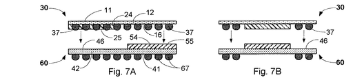
結合された相補的なパッケージ30と60とのユニットの構成は、図7(A)乃至図8(B)の平面図に例示される。図7(A)(側面図)と図7(B)(正面図)とにおいて、第1パッケージ30は、第2パッケージに対して逆向きとされ、第1パッケージ基板12のダイ実装面のはんだボール37が第2パッケージ基板42のダイ実装面のボールパッド(図示しない)と位置合わせされるように、そして第1パッケージ30のモールドキャップ表面25が第2基板42のダイ実装面の空領域46と位置合わせされるように、更に第2パッケージ60のモールドキャップ表面55が第1基板30のダイ実装面の空領域16と位置合わせされるように、位置合わせされて示されている。パッケージの取り扱いは、従来のパッケージアセンブリ機器を用いてなされてもよい。例えば、第2パッケージ60は、サポートに配置することができ、そして、第1パッケージは、ピック・アンド・プレイスツールを用いて、適切な位置に操作されることができる。一度位置合わせされると、第1パッケージ30のはんだボールが第2パッケージ基板46のパッドに接触するまで、図の矢印で示すように、相補的なパッケージは接合される。この時点で、相補的なパッケージペアユニットは完全である。ユニットは、はんだボール37を再び溶かし、パッケージのペアの電気的な相互接続を形成するために熱せられてもよい。ボールは、図8(A)及び(B)のユニットアセンブリ80において崩れた後に再び溶かしたものとなる。そのとき、ダイ25と55とはんだボール37との周囲の基板12と42との間のスペースを、図9(A)及び(B)にて示す95で満たすように、アセンブリはカプセル化され得る。これによって、2つの相補的なパッケージを有するモジュール90が完成する。モジュールは、「upper」表面91を有し、図9(A)と図9(B)とにおいて97で示す第2パッケージのはんだボールは、例えばマザーボードのようなモバイル・コンピューティングまたは通信製品において使用されるデバイスを備えるモジュール90の電気的な相互接続を形成する。
The unit configuration of the combined
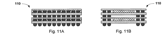
図8(A)及び(B)に示すユニット80のような相補的なパッケージペアユニットは、4つ以上のパッケージを有するモジュールを形成するためにスタックされる。図10(A)乃至図12(B)は、2つの相補的なパッケージペアユニット80,80’を、一方を他方の上にスタックすることによるモジュール120の構成を例示する。図10(A)及び(B)において、例えば図7(A)乃至図8(B)に示すような構成の相補的なパッケージペアユニット80,80’は、パッケージユニット80’の相互接続はんだボール67’がパッケージユニット80のパッケージ30の基板12のランド面11のボールパッド(図示しない)と位置合わせされるようにして位置合わせされる。図の矢印で示すように、はんだボール67’がパッドに接触するまで、ユニットは接合される。これは、4パッケージアセンブリを形成する。アセンブリは、はんだボール67’をリフローするように熱せられて、2つのユニット80,80’間の電気的な相互接続を形成する。
ボールは、図11(A)及び(B)の4パッケージアセンブリ110において崩れた後に再び溶かしたものとなる。そのとき、ダイとはんだボールとの周囲の基板の間のスペースを、図12(A)及び(B)にて示す125で満たすように、アセンブリはカプセル化され得る。これによって、2つの相補的なパッケージを有するモジュール120が完成する。モジュールは、「upper」表面121を有し、図11(A)及び(B)において127で示す最下パッケージのはんだボールは、例えばマザーボードのようなモバイル・コンピューティング又は通信機器において使用されるデバイスを備えるモジュール120の電気的な相互接続を形成する。はんだ再溶解は、単一の再溶解ステップにおけるすべてのはんだボール相互接続について実行できる。
Complementary package pair units, such as the
The balls are melted again after breaking in the four
他の形態は本発明の範囲にある。例えば、相補的なパッケージ上のそれぞれのダイが、ほぼ同じ寸法であるとして図に示されているが、それぞれのダイは、他の形態において異なる厚さ又は面積を有してもよく、特に、ダイは異なる機能を有してもよい。そして、例えば、相補的なパッケージのそれぞれの基板が、同じ長さと幅とを有するとして図に説明されているけれども、それぞれの基板は、他の形態において異なる面積を有してもよい。何れにしても、各基板のダイ実装面の空領域は、十分に大きくなければならず、しかもダイ又は相補的なパッケージにおけるダイ上のモールド体の表面の長さと幅とを適合させるように設定されなければならない。 Other forms are within the scope of the present invention. For example, although each die on a complementary package is shown in the figure as having approximately the same dimensions, each die may have a different thickness or area in other configurations, particularly The dies may have different functions. And for example, although each substrate in a complementary package is illustrated in the figure as having the same length and width, each substrate may have a different area in other configurations. In any case, the vacant area on the die mounting surface of each substrate must be sufficiently large and set to match the length and width of the surface of the mold body on the die or in a complementary package. It must be.
マルチパッケージモジュールは、さまざまな電子機器の何れにも有益であり、高いデバイス密度が望ましい場合、及び、デバイスアセンブリの寸法(面積、厚さ)を適合させるために製品内に制限されたスペースがある場合に、特に有益である。そのような製品には、例えば、携帯電話とパーソナル携帯情報端末、ラップトップ・コンピュータ、デジタルカメラ、及び電子エンターテインメント製品などのポータブル通信デバイスが含まれる。 Multi-package modules are useful for any of a variety of electronics, where high device density is desired, and there is limited space within the product to accommodate the dimensions (area, thickness) of the device assembly It is especially beneficial when. Such products include, for example, portable communication devices such as cell phones and personal digital assistants, laptop computers, digital cameras, and electronic entertainment products.
12,42…基板、13,43…ダイ実装面、14,44…ダイ、15,45…ダイ取付領域、16,46…空領域、24,54…モールド体 12, 42 ... Substrate, 13, 43 ... Die mounting surface, 14, 44 ... Die, 15, 45 ... Die mounting area, 16, 46 ... Empty area, 24, 54 ... Mold body
Claims (27)
第1基板のダイ実装面のダイ取付領域にダイが取付けられた第1パッケージと、
第1基板のダイ実装面上のボールパッドにマウントされた第1Z相互接続はんだボールと、
を具備する第1半導体チップパッケージと;
ダイ実装面とランド面とを具備し、ダイ実装面がダイ取付領域と空領域とを有する第2基板と、
第1基板のダイ実装面のダイ取付領域にダイが取付けられた第2パッケージと、
を具備する第2半導体チップパッケージとを備え;
第1パッケージは、第1パッケージのダイ実装面が第2パッケージのダイ実装面に面するように第2パッケージにスタックされ、第1パッケージのダイ取付領域は、第2パッケージの空領域と位置合わせされ、第1パッケージの第1Z相互接続はんだボールは、第2基板のダイ実装面上のボールパッドに接触するように構成されていることを特徴とする相補的なパッケージペアユニット。 A first substrate having a die mounting surface and a land surface, the die mounting surface having a die attachment region and an empty region;
A first package in which a die is attached to a die attachment region of the die mounting surface of the first substrate;
A first Z interconnect solder ball mounted on a ball pad on the die mounting surface of the first substrate;
A first semiconductor chip package comprising:
A second substrate having a die mounting surface and a land surface, the die mounting surface having a die attachment region and an empty region;
A second package in which a die is attached to the die attachment region of the die mounting surface of the first substrate;
A second semiconductor chip package comprising:
The first package is stacked on the second package so that the die mounting surface of the first package faces the die mounting surface of the second package, and the die mounting area of the first package is aligned with the empty area of the second package A complementary package pair unit, wherein the first Z interconnect solder balls of the first package are configured to contact the ball pads on the die mounting surface of the second substrate.
ダイ実装面とランド面とを具備し、ダイ実装面がダイ取付領域と空領域とを有する第3基板と、
第1基板のダイ実装面のダイ取付領域にダイが取付けられた第3パッケージと、
第1基板のダイ実装面上のボールパッドにマウントされた第3Z相互接続はんだボールと;
を具備する第3半導体チップパッケージと、
ダイ実装面とランド面とを具備し、ダイ実装面がダイ取付領域と空領域とを有する第4基板と、
第1基板のダイ実装面のダイ取付領域にダイが取付けられた第4パッケージと、
を具備する第4半導体チップパッケージと;
を有する第2の相補的なパッケージペアユニットとを備え:
第3パッケージは、第3パッケージのダイ実装面が第4パッケージのダイ実装面に面するように第4パッケージにスタックされ、第3パッケージのダイ取付領域は、第4パッケージの空領域と位置合わせされ、第3パッケージの第3Z相互接続はんだボールは、第4基板のダイ実装面上のボールパッドに接触し、更に、第1の相補的なパッケージペアユニットは、第2の相補的なパッケージペアユニットにスタックされ、第2パッケージの第2Z相互接続はんだボールは、第3パッケージ基板のランド面上のボールパッドに接触するように構成されていることを特徴とするマルチパッケージモジュール。 A first complementary package pair unit according to claim 10;
A third substrate having a die mounting surface and a land surface, the die mounting surface having a die mounting region and an empty region;
A third package in which a die is attached to the die attachment region of the die mounting surface of the first substrate;
A third Z interconnect solder ball mounted on a ball pad on the die mounting surface of the first substrate;
A third semiconductor chip package comprising:
A fourth substrate having a die mounting surface and a land surface, the die mounting surface having a die attachment region and an empty region;
A fourth package in which the die is attached to the die attachment region of the die mounting surface of the first substrate;
A fourth semiconductor chip package comprising:
With a second complementary package pair unit having:
The third package is stacked on the fourth package such that the die mounting surface of the third package faces the die mounting surface of the fourth package, and the die mounting area of the third package is aligned with the empty area of the fourth package The third Z interconnect solder balls of the third package are in contact with the ball pads on the die mounting surface of the fourth substrate, and the first complementary package pair unit is the second complementary package pair. A multi-package module, characterized in that the second Z interconnect solder balls of the second package are configured to contact the ball pads on the land surface of the third package substrate, stacked in the unit.
ダイのアクティブ面上にダイパッドを備える半導体ダイを形成するダイ形成工程と、
基板の第1面のダイ取付領域にダイをマウントするダイ実装工程と第1の模様付けられた金属層ボンドパッドにダイを電気的に相互接続する相互接続工程と、
を備えることを特徴とする半導体チップパッケージの製造方法。 A package substrate forming step comprising: forming a package substrate comprising a first patterned metal layer on the first surface, the package substrate comprising a first patterned metal layer on the first surface, and a second patterned metal layer on the second surface;
A die forming step of forming a semiconductor die having a die pad on the active surface of the die;
A die mounting step of mounting the die on the die attachment region of the first surface of the substrate and an interconnection step of electrically interconnecting the die to the first patterned metal layer bond pad;
A method of manufacturing a semiconductor chip package, comprising:
第1パッケージ基板の第1面上のボールパッドに第1Z相互接続はんだボールをマウントするはんだボール実装工程と;
各パッケージ基板の第1面が他のパッケージ基板の第1面に面し、各パッケージ基板のダイ取付領域が他のパッケージ基板の空領域に一致するように、第1及び第2パッケージを互いに関連付けて位置合わせする位置合わせ工程と;
第2パッケージ基板の第1面上のボールパッドにて第1Z相互接続はんだボールが接触するはんだボール接触工程と;
第2パッケージ基板の第1面上のボールパッドと電気的な接続関係をもたらすために第1Z相互接続はんだボールをリフローするリフロー工程と、
を備えることを特徴とするマルチパッケージモジュールの製造方法。 A first and second semiconductor chip package forming step of forming the first and second semiconductor chip packages according to claim 1;
A solder ball mounting step of mounting a first Z interconnect solder ball on a ball pad on the first surface of the first package substrate;
Associate the first and second packages with each other so that the first surface of each package substrate faces the first surface of the other package substrate and the die mounting area of each package substrate coincides with the empty area of the other package substrate An alignment step of aligning and
A solder ball contact step in which the first Z interconnect solder balls contact at a ball pad on the first surface of the second package substrate;
A reflow process for reflowing the first Z interconnect solder balls to provide an electrical connection with the ball pads on the first surface of the second package substrate;
A method of manufacturing a multi-package module comprising:
第1パッケージ基板の第1面上のボールパッドに第1Z相互接続はんだボールをマウントするはんだボール実装工程と;
互いに面するパッケージのダイ実装面と他方のパッケージ基板の空領域に位置合わせされた各パッケージのダイ取付領域とによって、第2パッケージの上に第1パッケージをスタックする第1パッケージスタック工程と;
第2パッケージ基板の第1面上のボールパッドと電気的な接続関係をもたらすために第1Z相互接続はんだボールをリフローするリフロー工程と、
を備えることを特徴とするマルチパッケージモジュールの製造方法。 First and second package forming steps for forming the first and second packages according to claim 1;
A solder ball mounting step of mounting a first Z interconnect solder ball on a ball pad on the first surface of the first package substrate;
A first package stacking step of stacking the first package on the second package by means of a die mounting surface of the package facing each other and a die attachment region of each package aligned with an empty region of the other package substrate;
A reflow process for reflowing the first Z interconnect solder balls to provide an electrical connection with the ball pads on the first surface of the second package substrate;
A method of manufacturing a multi-package module comprising:
Applications Claiming Priority (4)
| Application Number | Priority Date | Filing Date | Title |
|---|---|---|---|
| US67044305P | 2005-04-11 | 2005-04-11 | |
| US60/670,443 | 2005-04-11 | ||
| US11/394,363 US7545031B2 (en) | 2005-04-11 | 2006-03-30 | Multipackage module having stacked packages with asymmetrically arranged die and molding |
| US11/394,363 | 2006-03-30 |
Publications (2)
| Publication Number | Publication Date |
|---|---|
| JP2006295183A true JP2006295183A (en) | 2006-10-26 |
| JP5394603B2 JP5394603B2 (en) | 2014-01-22 |
Family
ID=37082414
Family Applications (1)
| Application Number | Title | Priority Date | Filing Date |
|---|---|---|---|
| JP2006108295A Expired - Lifetime JP5394603B2 (en) | 2005-04-11 | 2006-04-11 | A multi-package module comprising a stacked package comprising a die and a mold body arranged asymmetrically. |
Country Status (4)
| Country | Link |
|---|---|
| US (2) | US7545031B2 (en) |
| JP (1) | JP5394603B2 (en) |
| KR (3) | KR101227792B1 (en) |
| TW (1) | TWI404190B (en) |
Cited By (1)
| Publication number | Priority date | Publication date | Assignee | Title |
|---|---|---|---|---|
| WO2009055069A3 (en) * | 2007-10-25 | 2009-06-04 | Chipstack Inc | Multiple package module using a rigid flex printed circuit board |
Families Citing this family (8)
| Publication number | Priority date | Publication date | Assignee | Title |
|---|---|---|---|---|
| US7545031B2 (en) * | 2005-04-11 | 2009-06-09 | Stats Chippac Ltd. | Multipackage module having stacked packages with asymmetrically arranged die and molding |
| SG149725A1 (en) * | 2007-07-24 | 2009-02-27 | Micron Technology Inc | Thin semiconductor die packages and associated systems and methods |
| SG149724A1 (en) | 2007-07-24 | 2009-02-27 | Micron Technology Inc | Semicoductor dies with recesses, associated leadframes, and associated systems and methods |
| TWI385779B (en) * | 2009-10-28 | 2013-02-11 | 財團法人國家實驗研究院國家晶片系統設計中心 | Multi-layer system chip module structure |
| KR101881732B1 (en) * | 2011-06-30 | 2018-07-27 | 무라타 일렉트로닉스 오와이 | A method of making a system-in-package device, and a system-in-package device |
| KR102032887B1 (en) * | 2012-12-10 | 2019-10-16 | 삼성전자 주식회사 | Semiconductor package and method for routing the package |
| US10068866B2 (en) * | 2016-09-29 | 2018-09-04 | Intel Corporation | Integrated circuit package having rectangular aspect ratio |
| US11171108B2 (en) * | 2018-10-04 | 2021-11-09 | Advanced Semiconductor Engineering, Inc. | Semiconductor package and method for manufacturing the same |
Citations (6)
| Publication number | Priority date | Publication date | Assignee | Title |
|---|---|---|---|---|
| JPH0613541A (en) * | 1992-03-02 | 1994-01-21 | Motorola Inc | Stackable three-dimensional multi-chip semiconductor device and its manufacturing method |
| JP2001210954A (en) * | 2000-01-24 | 2001-08-03 | Ibiden Co Ltd | Multilayer board |
| JP2001223297A (en) * | 1999-11-30 | 2001-08-17 | Fujitsu Ltd | Semiconductor device, method of manufacturing semiconductor device, and method of stacking semiconductor device |
| JP2003197849A (en) * | 2001-10-18 | 2003-07-11 | Matsushita Electric Ind Co Ltd | Component built-in module and manufacturing method thereof |
| JP2003204167A (en) * | 2001-10-26 | 2003-07-18 | Matsushita Electric Works Ltd | Sheet material for circuit board and manufacturing method thereof, and multilayer board and manufacturing method thereof |
| JP2006080564A (en) * | 2005-11-21 | 2006-03-23 | Genusion:Kk | Package structure of semiconductor device |
Family Cites Families (29)
| Publication number | Priority date | Publication date | Assignee | Title |
|---|---|---|---|---|
| JPH10294423A (en) * | 1997-04-17 | 1998-11-04 | Nec Corp | Semiconductor device |
| US6414391B1 (en) * | 1998-06-30 | 2002-07-02 | Micron Technology, Inc. | Module assembly for stacked BGA packages with a common bus bar in the assembly |
| US5854507A (en) * | 1998-07-21 | 1998-12-29 | Hewlett-Packard Company | Multiple chip assembly |
| SG75873A1 (en) * | 1998-09-01 | 2000-10-24 | Texas Instr Singapore Pte Ltd | Stacked flip-chip integrated circuit assemblage |
| US6122171A (en) * | 1999-07-30 | 2000-09-19 | Micron Technology, Inc. | Heat sink chip package and method of making |
| EP1085572A3 (en) * | 1999-09-16 | 2006-04-19 | Texas Instruments Incorporated | Low pass filter integral with semiconductor package |
| KR100673378B1 (en) * | 1999-12-17 | 2007-01-23 | 삼성전자주식회사 | Chip scale multilayer chip package and its manufacturing method |
| US6369448B1 (en) * | 2000-01-21 | 2002-04-09 | Lsi Logic Corporation | Vertically integrated flip chip semiconductor package |
| JP3980807B2 (en) * | 2000-03-27 | 2007-09-26 | 株式会社東芝 | Semiconductor device and semiconductor module |
| US7247932B1 (en) * | 2000-05-19 | 2007-07-24 | Megica Corporation | Chip package with capacitor |
| US6778404B1 (en) * | 2000-06-02 | 2004-08-17 | Micron Technology Inc | Stackable ball grid array |
| JP2001352035A (en) * | 2000-06-07 | 2001-12-21 | Sony Corp | Assembly jig for multilayer semiconductor device and method for manufacturing multilayer semiconductor device |
| US6404043B1 (en) * | 2000-06-21 | 2002-06-11 | Dense-Pac Microsystems, Inc. | Panel stacking of BGA devices to form three-dimensional modules |
| SG95637A1 (en) * | 2001-03-15 | 2003-04-23 | Micron Technology Inc | Semiconductor/printed circuit board assembly, and computer system |
| TWI255532B (en) * | 2002-02-05 | 2006-05-21 | Siliconware Precision Industries Co Ltd | Flip-chip ball grid array semiconductor package with heat-dissipating device and method for fabricating the same |
| US7479407B2 (en) * | 2002-11-22 | 2009-01-20 | Freescale Semiconductor, Inc. | Digital and RF system and method therefor |
| TWI290757B (en) * | 2002-12-30 | 2007-12-01 | Advanced Semiconductor Eng | Thermal enhance MCM package and the manufacturing method thereof |
| TW576549U (en) * | 2003-04-04 | 2004-02-11 | Advanced Semiconductor Eng | Multi-chip package combining wire-bonding and flip-chip configuration |
| JP3842759B2 (en) * | 2003-06-12 | 2006-11-08 | 株式会社東芝 | 3D mounting semiconductor module and 3D mounting semiconductor system |
| JP4330411B2 (en) * | 2003-09-24 | 2009-09-16 | 三洋電機株式会社 | Circuit equipment |
| JP4204989B2 (en) * | 2004-01-30 | 2009-01-07 | 新光電気工業株式会社 | Semiconductor device and manufacturing method thereof |
| KR100627006B1 (en) * | 2004-04-01 | 2006-09-25 | 삼성전자주식회사 | Indent chips, semiconductor packages and multi-chip packages using the same |
| TWI237882B (en) * | 2004-05-11 | 2005-08-11 | Via Tech Inc | Stacked multi-chip package |
| JP2006114604A (en) * | 2004-10-13 | 2006-04-27 | Toshiba Corp | Semiconductor device and assembly method thereof |
| KR100622609B1 (en) | 2005-02-16 | 2006-09-19 | 주식회사 하이닉스반도체 | Thin Film Formation Method |
| JP4557757B2 (en) * | 2005-03-14 | 2010-10-06 | 株式会社東芝 | Semiconductor device |
| US7545031B2 (en) * | 2005-04-11 | 2009-06-09 | Stats Chippac Ltd. | Multipackage module having stacked packages with asymmetrically arranged die and molding |
| US20070108583A1 (en) * | 2005-08-08 | 2007-05-17 | Stats Chippac Ltd. | Integrated circuit package-on-package stacking system |
| US20070210433A1 (en) * | 2006-03-08 | 2007-09-13 | Rajesh Subraya | Integrated device having a plurality of chip arrangements and method for producing the same |
-
2006
- 2006-03-30 US US11/394,363 patent/US7545031B2/en active Active
- 2006-04-11 JP JP2006108295A patent/JP5394603B2/en not_active Expired - Lifetime
- 2006-04-11 TW TW095112891A patent/TWI404190B/en active
- 2006-04-11 KR KR1020060032536A patent/KR101227792B1/en not_active Expired - Lifetime
-
2009
- 2009-04-30 US US12/433,852 patent/US7932593B2/en not_active Expired - Lifetime
-
2011
- 2011-12-05 KR KR1020110128710A patent/KR101245454B1/en not_active Expired - Lifetime
-
2012
- 2012-06-25 KR KR1020120067730A patent/KR101299852B1/en active Active
Patent Citations (6)
| Publication number | Priority date | Publication date | Assignee | Title |
|---|---|---|---|---|
| JPH0613541A (en) * | 1992-03-02 | 1994-01-21 | Motorola Inc | Stackable three-dimensional multi-chip semiconductor device and its manufacturing method |
| JP2001223297A (en) * | 1999-11-30 | 2001-08-17 | Fujitsu Ltd | Semiconductor device, method of manufacturing semiconductor device, and method of stacking semiconductor device |
| JP2001210954A (en) * | 2000-01-24 | 2001-08-03 | Ibiden Co Ltd | Multilayer board |
| JP2003197849A (en) * | 2001-10-18 | 2003-07-11 | Matsushita Electric Ind Co Ltd | Component built-in module and manufacturing method thereof |
| JP2003204167A (en) * | 2001-10-26 | 2003-07-18 | Matsushita Electric Works Ltd | Sheet material for circuit board and manufacturing method thereof, and multilayer board and manufacturing method thereof |
| JP2006080564A (en) * | 2005-11-21 | 2006-03-23 | Genusion:Kk | Package structure of semiconductor device |
Cited By (1)
| Publication number | Priority date | Publication date | Assignee | Title |
|---|---|---|---|---|
| WO2009055069A3 (en) * | 2007-10-25 | 2009-06-04 | Chipstack Inc | Multiple package module using a rigid flex printed circuit board |
Also Published As
| Publication number | Publication date |
|---|---|
| KR20060107938A (en) | 2006-10-16 |
| KR20120009413A (en) | 2012-01-31 |
| US7932593B2 (en) | 2011-04-26 |
| JP5394603B2 (en) | 2014-01-22 |
| KR20120090875A (en) | 2012-08-17 |
| TW200644216A (en) | 2006-12-16 |
| KR101227792B1 (en) | 2013-01-29 |
| US20090218675A1 (en) | 2009-09-03 |
| KR101299852B1 (en) | 2013-08-23 |
| KR101245454B1 (en) | 2013-03-19 |
| US7545031B2 (en) | 2009-06-09 |
| US20060226528A1 (en) | 2006-10-12 |
| TWI404190B (en) | 2013-08-01 |
Similar Documents
| Publication | Publication Date | Title |
|---|---|---|
| US20250087550A1 (en) | Semiconductor package and manufacturing method thereof | |
| KR100493063B1 (en) | BGA package with stacked semiconductor chips and manufacturing method thereof | |
| US6841881B2 (en) | Semiconductor device and a method of manufacturing the same | |
| CN102867800B (en) | Functional chip is connected to packaging part to form package on package | |
| US7679178B2 (en) | Semiconductor package on which a semiconductor device can be stacked and fabrication method thereof | |
| US9190401B2 (en) | Stacked semiconductor packages | |
| US9030021B2 (en) | Printed circuit board having hexagonally aligned bump pads for substrate of semiconductor package, and semiconductor package including the same | |
| US20060240595A1 (en) | Method and apparatus for flip-chip packaging providing testing capability | |
| JP2015503850A (en) | Stackable microelectronic package structure | |
| KR101299852B1 (en) | Multipackage module having stacked packages with asymmetrically arranged die and molding | |
| JPWO2001026155A1 (en) | Semiconductor device and its manufacturing method, manufacturing device, circuit board, and electronic device | |
| JP2002252303A (en) | Flip chip semiconductor device in molded chip scale package and assembling method | |
| CN103208487A (en) | Methods and apparatus for thinner package on package structures | |
| KR20120058118A (en) | Method of fabricating stacked package, and method of mounting stacked package fabricated by the same | |
| JP2013021058A (en) | Manufacturing method of semiconductor device | |
| KR20140071561A (en) | Circuit board and semiconductor package including the same | |
| CN107546217A (en) | Method and structure for packaging and stacking pillar top interconnection | |
| CN101465341B (en) | Stacked chip packaging structure | |
| JP2004087936A (en) | Semiconductor device, method of manufacturing semiconductor device, and electronic apparatus | |
| TW201729369A (en) | Reinforced wire for offset bonding through-hole array | |
| CN100552940C (en) | Stack structure of semiconductor element embedded loading board | |
| CN221783207U (en) | Chip packaging structure and electronic equipment | |
| JP2006202997A (en) | Semiconductor device and manufacturing method thereof | |
| JP2005167159A (en) | Multilayer semiconductor device | |
| JP2003037244A (en) | Semiconductor device tape carrier and semiconductor device using the same |
Legal Events
| Date | Code | Title | Description |
|---|---|---|---|
| RD04 | Notification of resignation of power of attorney |
Free format text: JAPANESE INTERMEDIATE CODE: A7424 Effective date: 20080625 |
|
| A621 | Written request for application examination |
Free format text: JAPANESE INTERMEDIATE CODE: A621 Effective date: 20090408 |
|
| RD02 | Notification of acceptance of power of attorney |
Free format text: JAPANESE INTERMEDIATE CODE: A7422 Effective date: 20100810 |
|
| RD04 | Notification of resignation of power of attorney |
Free format text: JAPANESE INTERMEDIATE CODE: A7424 Effective date: 20100823 |
|
| A521 | Request for written amendment filed |
Free format text: JAPANESE INTERMEDIATE CODE: A821 Effective date: 20100810 |
|
| RD04 | Notification of resignation of power of attorney |
Free format text: JAPANESE INTERMEDIATE CODE: A7424 Effective date: 20100823 |
|
| A977 | Report on retrieval |
Free format text: JAPANESE INTERMEDIATE CODE: A971007 Effective date: 20110722 |
|
| A131 | Notification of reasons for refusal |
Free format text: JAPANESE INTERMEDIATE CODE: A131 Effective date: 20110802 |
|
| A601 | Written request for extension of time |
Free format text: JAPANESE INTERMEDIATE CODE: A601 Effective date: 20111031 |
|
| A602 | Written permission of extension of time |
Free format text: JAPANESE INTERMEDIATE CODE: A602 Effective date: 20111104 |
|
| A601 | Written request for extension of time |
Free format text: JAPANESE INTERMEDIATE CODE: A601 Effective date: 20111201 |
|
| A602 | Written permission of extension of time |
Free format text: JAPANESE INTERMEDIATE CODE: A602 Effective date: 20111206 |
|
| A521 | Request for written amendment filed |
Free format text: JAPANESE INTERMEDIATE CODE: A523 Effective date: 20111228 |
|
| A02 | Decision of refusal |
Free format text: JAPANESE INTERMEDIATE CODE: A02 Effective date: 20120717 |
|
| A521 | Request for written amendment filed |
Free format text: JAPANESE INTERMEDIATE CODE: A523 Effective date: 20121119 |
|
| A911 | Transfer to examiner for re-examination before appeal (zenchi) |
Free format text: JAPANESE INTERMEDIATE CODE: A911 Effective date: 20121205 |
|
| A912 | Re-examination (zenchi) completed and case transferred to appeal board |
Free format text: JAPANESE INTERMEDIATE CODE: A912 Effective date: 20121228 |
|
| A521 | Request for written amendment filed |
Free format text: JAPANESE INTERMEDIATE CODE: A523 Effective date: 20130828 |
|
| A61 | First payment of annual fees (during grant procedure) |
Free format text: JAPANESE INTERMEDIATE CODE: A61 Effective date: 20131017 |
|
| R150 | Certificate of patent or registration of utility model |
Ref document number: 5394603 Country of ref document: JP Free format text: JAPANESE INTERMEDIATE CODE: R150 Free format text: JAPANESE INTERMEDIATE CODE: R150 |
|
| R250 | Receipt of annual fees |
Free format text: JAPANESE INTERMEDIATE CODE: R250 |
|
| R250 | Receipt of annual fees |
Free format text: JAPANESE INTERMEDIATE CODE: R250 |
|
| R250 | Receipt of annual fees |
Free format text: JAPANESE INTERMEDIATE CODE: R250 |
|
| R250 | Receipt of annual fees |
Free format text: JAPANESE INTERMEDIATE CODE: R250 |
|
| R250 | Receipt of annual fees |
Free format text: JAPANESE INTERMEDIATE CODE: R250 |
|
| R250 | Receipt of annual fees |
Free format text: JAPANESE INTERMEDIATE CODE: R250 |
|
| R250 | Receipt of annual fees |
Free format text: JAPANESE INTERMEDIATE CODE: R250 |
|
| R250 | Receipt of annual fees |
Free format text: JAPANESE INTERMEDIATE CODE: R250 |
|
| S531 | Written request for registration of change of domicile |
Free format text: JAPANESE INTERMEDIATE CODE: R313531 |
|
| S533 | Written request for registration of change of name |
Free format text: JAPANESE INTERMEDIATE CODE: R313533 |
|
| R350 | Written notification of registration of transfer |
Free format text: JAPANESE INTERMEDIATE CODE: R350 |
|
| R250 | Receipt of annual fees |
Free format text: JAPANESE INTERMEDIATE CODE: R250 |
|
| S111 | Request for change of ownership or part of ownership |
Free format text: JAPANESE INTERMEDIATE CODE: R313113 |
|
| R250 | Receipt of annual fees |
Free format text: JAPANESE INTERMEDIATE CODE: R250 |
|
| R350 | Written notification of registration of transfer |
Free format text: JAPANESE INTERMEDIATE CODE: R350 |