JP2006295193A - System and method for reducing simultaneous switching noise in integrated circuits - Google Patents
System and method for reducing simultaneous switching noise in integrated circuits Download PDFInfo
- Publication number
- JP2006295193A JP2006295193A JP2006110403A JP2006110403A JP2006295193A JP 2006295193 A JP2006295193 A JP 2006295193A JP 2006110403 A JP2006110403 A JP 2006110403A JP 2006110403 A JP2006110403 A JP 2006110403A JP 2006295193 A JP2006295193 A JP 2006295193A
- Authority
- JP
- Japan
- Prior art keywords
- integrated circuit
- circuit board
- decoupling capacitor
- substrate
- die
- Prior art date
- Legal status (The legal status is an assumption and is not a legal conclusion. Google has not performed a legal analysis and makes no representation as to the accuracy of the status listed.)
- Granted
Links
Images










Classifications
-
- H—ELECTRICITY
- H10—SEMICONDUCTOR DEVICES; ELECTRIC SOLID-STATE DEVICES NOT OTHERWISE PROVIDED FOR
- H10W—GENERIC PACKAGES, INTERCONNECTIONS, CONNECTORS OR OTHER CONSTRUCTIONAL DETAILS OF DEVICES COVERED BY CLASS H10
- H10W72/00—Interconnections or connectors in packages
-
- H—ELECTRICITY
- H05—ELECTRIC TECHNIQUES NOT OTHERWISE PROVIDED FOR
- H05K—PRINTED CIRCUITS; CASINGS OR CONSTRUCTIONAL DETAILS OF ELECTRIC APPARATUS; MANUFACTURE OF ASSEMBLAGES OF ELECTRICAL COMPONENTS
- H05K1/00—Printed circuits
- H05K1/02—Details
- H05K1/0213—Electrical arrangements not otherwise provided for
- H05K1/0216—Reduction of cross-talk, noise or electromagnetic interference
- H05K1/023—Reduction of cross-talk, noise or electromagnetic interference using auxiliary mounted passive components or auxiliary substances
- H05K1/0231—Capacitors or dielectric substances
-
- H—ELECTRICITY
- H10—SEMICONDUCTOR DEVICES; ELECTRIC SOLID-STATE DEVICES NOT OTHERWISE PROVIDED FOR
- H10W—GENERIC PACKAGES, INTERCONNECTIONS, CONNECTORS OR OTHER CONSTRUCTIONAL DETAILS OF DEVICES COVERED BY CLASS H10
- H10W42/00—Arrangements for protection of devices
- H10W42/121—Arrangements for protection of devices protecting against mechanical damage
-
- H—ELECTRICITY
- H10—SEMICONDUCTOR DEVICES; ELECTRIC SOLID-STATE DEVICES NOT OTHERWISE PROVIDED FOR
- H10W—GENERIC PACKAGES, INTERCONNECTIONS, CONNECTORS OR OTHER CONSTRUCTIONAL DETAILS OF DEVICES COVERED BY CLASS H10
- H10W70/00—Package substrates; Interposers; Redistribution layers [RDL]
- H10W70/60—Insulating or insulated package substrates; Interposers; Redistribution layers
- H10W70/62—Insulating or insulated package substrates; Interposers; Redistribution layers characterised by their interconnections
- H10W70/65—Shapes or dispositions of interconnections
-
- H—ELECTRICITY
- H10—SEMICONDUCTOR DEVICES; ELECTRIC SOLID-STATE DEVICES NOT OTHERWISE PROVIDED FOR
- H10W—GENERIC PACKAGES, INTERCONNECTIONS, CONNECTORS OR OTHER CONSTRUCTIONAL DETAILS OF DEVICES COVERED BY CLASS H10
- H10W70/00—Package substrates; Interposers; Redistribution layers [RDL]
- H10W70/60—Insulating or insulated package substrates; Interposers; Redistribution layers
- H10W70/67—Insulating or insulated package substrates; Interposers; Redistribution layers characterised by their insulating layers or insulating parts
- H10W70/68—Shapes or dispositions thereof
-
- H—ELECTRICITY
- H05—ELECTRIC TECHNIQUES NOT OTHERWISE PROVIDED FOR
- H05K—PRINTED CIRCUITS; CASINGS OR CONSTRUCTIONAL DETAILS OF ELECTRIC APPARATUS; MANUFACTURE OF ASSEMBLAGES OF ELECTRICAL COMPONENTS
- H05K1/00—Printed circuits
- H05K1/18—Printed circuits structurally associated with non-printed electric components
- H05K1/182—Printed circuits structurally associated with non-printed electric components associated with components mounted in printed circuit boards [PCB], e.g. insert-mounted components [IMC]
-
- H—ELECTRICITY
- H05—ELECTRIC TECHNIQUES NOT OTHERWISE PROVIDED FOR
- H05K—PRINTED CIRCUITS; CASINGS OR CONSTRUCTIONAL DETAILS OF ELECTRIC APPARATUS; MANUFACTURE OF ASSEMBLAGES OF ELECTRICAL COMPONENTS
- H05K2201/00—Indexing scheme relating to printed circuits covered by H05K1/00
- H05K2201/09—Shape and layout
- H05K2201/09009—Substrate related
- H05K2201/09072—Hole or recess under component or special relationship between hole and component
-
- H—ELECTRICITY
- H05—ELECTRIC TECHNIQUES NOT OTHERWISE PROVIDED FOR
- H05K—PRINTED CIRCUITS; CASINGS OR CONSTRUCTIONAL DETAILS OF ELECTRIC APPARATUS; MANUFACTURE OF ASSEMBLAGES OF ELECTRICAL COMPONENTS
- H05K2201/00—Indexing scheme relating to printed circuits covered by H05K1/00
- H05K2201/10—Details of components or other objects attached to or integrated in a printed circuit board
- H05K2201/10431—Details of mounted components
- H05K2201/10507—Involving several components
- H05K2201/1053—Mounted components directly electrically connected to each other, i.e. not via the PCB
-
- H—ELECTRICITY
- H05—ELECTRIC TECHNIQUES NOT OTHERWISE PROVIDED FOR
- H05K—PRINTED CIRCUITS; CASINGS OR CONSTRUCTIONAL DETAILS OF ELECTRIC APPARATUS; MANUFACTURE OF ASSEMBLAGES OF ELECTRICAL COMPONENTS
- H05K2201/00—Indexing scheme relating to printed circuits covered by H05K1/00
- H05K2201/10—Details of components or other objects attached to or integrated in a printed circuit board
- H05K2201/10613—Details of electrical connections of non-printed components, e.g. special leads
- H05K2201/10621—Components characterised by their electrical contacts
- H05K2201/10734—Ball grid array [BGA]; Bump grid array
Landscapes
- Physics & Mathematics (AREA)
- Electromagnetism (AREA)
- Engineering & Computer Science (AREA)
- Microelectronics & Electronic Packaging (AREA)
- Semiconductor Integrated Circuits (AREA)
- Structures For Mounting Electric Components On Printed Circuit Boards (AREA)
- Cooling Or The Like Of Semiconductors Or Solid State Devices (AREA)
Abstract
【課題】集積回路と共に使用されるヒートシンク/スプレッダの有効性を減少させることなく、集積回路におけるスイッチングノイズを減少させる。
【解決手段】デバイスは、集積回路510と、集積回路510に外部的に接続された1つ以上のデカップリングキャパシタ540と、を具備する。デカップリングキャパシタ540は、集積回路510内の1つ以上のホットスポット520、521においてより高い濃度となるように配置される。
【選択図】 図5CSwitching noise in an integrated circuit is reduced without reducing the effectiveness of a heat sink / spreader used with the integrated circuit.
The device includes an integrated circuit (510) and one or more decoupling capacitors (540) externally connected to the integrated circuit (510). The decoupling capacitor 540 is arranged to have a higher concentration at one or more hot spots 520 521 in the integrated circuit 510.
[Selection] Figure 5C
Description
本発明は、一般的には集積回路に関し、特に、集積回路内のホットスポットの近傍により高い濃度で位置するようにデカップリングキャパシタを配設することにより、集積回路内の同時的スイッチングノイズを減少させるためのシステム及び方法に関する。 The present invention relates generally to integrated circuits and, in particular, reduces simultaneous switching noise in integrated circuits by placing decoupling capacitors so that they are located at higher concentrations near hot spots in integrated circuits. The present invention relates to a system and method.
コンピュータ関連技術の発展に伴い、技術の進歩は、速度及び処理能力の向上に対する要請に適合するようになされている。これにより、集積回路は、次第に、より小さい回路構成部品をより多く有することとなっている。集積回路は、一般的に多数のトランジスタを含み、これらにより、集積回路内で種々の論理ゲート、ラッチ、増幅器、及び他の構成部品が形成される。 With the development of computer-related technology, technological advances are adapted to meet the demand for increased speed and processing power. Thereby, the integrated circuit will gradually have more smaller circuit components. Integrated circuits typically include a large number of transistors, which form various logic gates, latches, amplifiers, and other components within the integrated circuit.
集積回路の複雑さが増すと共に、集積回路内の構成部品の数が増加するのにつれ、設計者は、従前の複雑でない回路ではそれほど深刻ではなかった或いは存在しなかった問題にしばしば直面する。例えば、集積回路内のトランジスタの数が増加するのにつれ、トランジスタによって生成される同時的スイッチングノイズの量も通常増加する。このスイッチングノイズは、集積回路の性能を低下させる、或いは正常な機能を阻害する可能性がある。 As the complexity of integrated circuits increases and the number of components in an integrated circuit increases, designers often face problems that were not so serious or existed in previous uncomplicated circuits. For example, as the number of transistors in an integrated circuit increases, the amount of simultaneous switching noise generated by the transistors typically increases. This switching noise can degrade the performance of the integrated circuit or impair normal function.
従来的には、スイッチングノイズの増加の問題は、デカップリングキャパシタを集積回路に接続することにより処理される。通常、デカップリングキャパシタは、集積回路パッケージの外部に配置され、各デカップリングキャパシタのリードの一方が集積回路内の接地面に接続され、他方のリードが集積回路内のパワー面に接続される。 Traditionally, the problem of increased switching noise is addressed by connecting a decoupling capacitor to the integrated circuit. Typically, the decoupling capacitor is placed outside the integrated circuit package, with one of the leads of each decoupling capacitor connected to the ground plane in the integrated circuit and the other lead connected to the power plane in the integrated circuit.
従来的には、デカップリングキャパシタは、集積回路ダイスが形成される基板の下面上に配置される。これにより、デカップリングキャパシタを集積回路ダイスに近接して配置すると共に、集積回路ダイスにコンタクトしてヒートシンクまたはヒートスプレッダを配置することが可能となる。一般的に、複数のデカップリングキャパシタが、集積回路ダイスの下面上の領域の全体に亘って均等に分配される。デカップリングキャパシタの高さは、通常、集積回路とそれが実装される回路基盤との間のコネクタの高さよりも大きいため、回路基盤には、デカップリングキャパシタが延在できるような孔を形成する必要がある。 Conventionally, the decoupling capacitor is disposed on the lower surface of the substrate on which the integrated circuit die is formed. This makes it possible to place the decoupling capacitor close to the integrated circuit die and to place a heat sink or heat spreader in contact with the integrated circuit die. In general, a plurality of decoupling capacitors are evenly distributed over the entire area on the bottom surface of the integrated circuit die. Since the height of the decoupling capacitor is usually larger than the height of the connector between the integrated circuit and the circuit board on which it is mounted, a hole is formed in the circuit board so that the decoupling capacitor can extend. There is a need.
この従来技術は、集積回路内のスイッチングノイズを確かに減少させるが、幾つかの欠点を有する。例えば、回路基盤内の孔により、ヒートシンク/スプレッダからの圧力下で集積回路が屈曲する可能性があり、これは、集積回路とヒートシンク/スプレッダとの間の熱的コンタクトを減少させる。更に、集積回路の全体に亘るデカップリングキャパシタの均等分布は、スイッチングノイズの減少には最適ではない。 While this prior art certainly reduces switching noise in integrated circuits, it has several drawbacks. For example, holes in the circuit board can cause the integrated circuit to bend under pressure from the heat sink / spreader, which reduces the thermal contact between the integrated circuit and the heat sink / spreader. Furthermore, the uniform distribution of decoupling capacitors throughout the integrated circuit is not optimal for reducing switching noise.
上述の課題は、本発明の様々な実施形態によって解消することが可能である。概略的には、本発明は、集積回路と共に使用されるヒートシンク/スプレッダの有効性を減少させることなく、集積回路におけるスイッチングノイズを減少させるためのシステム及び方法を含む。一実施形態において、デカップリングキャパシタは、集積回路ダイスが実装される基板の下面から集積回路に接続される。デカップリングキャパシタは、均等に分布される代わりに、集積回路の「ホットスポット」領域においてより高い濃度で配置される。一実施形態において、デカップリングキャパシタ及び回路基盤の対応する孔(そこにデカップリングキャパシタが挿入される)は、集積回路の中心部分に対してサポートを提供するように配置され、これによって、集積回路がヒートシンク/スプレッダから離れるように屈曲するのを防止する。一実施形態において、集積回路内の異なる接地面及び/またはパワー面に接続されるビアの濃度は、他の領域よりもホットスポットで高くなるように設定される。 The above problems can be solved by various embodiments of the present invention. In general, the present invention includes a system and method for reducing switching noise in an integrated circuit without reducing the effectiveness of a heat sink / spreader used with the integrated circuit. In one embodiment, the decoupling capacitor is connected to the integrated circuit from the bottom surface of the substrate on which the integrated circuit die is mounted. Instead of being evenly distributed, the decoupling capacitors are placed at a higher concentration in the “hot spot” region of the integrated circuit. In one embodiment, the decoupling capacitors and corresponding holes in the circuit board (where the decoupling capacitors are inserted) are arranged to provide support for the central portion of the integrated circuit, thereby providing the integrated circuit. Prevents bending away from the heat sink / spreader. In one embodiment, the concentration of vias connected to different ground planes and / or power planes in an integrated circuit is set to be higher at hot spots than other areas.
一実施形態は、集積回路ダイス及び1つ以上のデカップリングキャパシタを含むデバイスからなる。デカップリングキャパシタは、集積回路ダイス内のホットスポットでデカップリングキャパシタがより高い濃度で存在するように、集積回路ダイスの各位置に外部的に接続される。一実施形態において、集積回路ダイスは基板上に実装されると共に、デカップリングキャパシタは基板を通して集積回路ダイスに接続される。基板は、貫通するように形成された1つ以上の孔を有する回路基盤に実装されることができる。孔は、基板が回路基盤に実装される時、デカップリングキャパシタが孔を通して延存するように配置される。回路基盤は、集積回路ダイスの中心部分の下側に位置する部分を含むことができ、基板上のコネクタがこの回路基盤の部分に支持される。デバイスはまた、集積回路ダイスと熱的コンタクトするように配置されたヒートシンク/スプレッダを含むことができる。ヒートシンク/スプレッダに圧力を付与するために、カップリング、例えば、裏板及び接続ピン、を使用することができ、これにより、集積回路ダイスとの熱的コンタクトを維持する。集積回路ダイスはまた、集積回路ダイスの接地及び/またはパワー面に接続されるビアを含むことができ、ここで、ビアの濃度は集積回路ダイスの他の領域よりもホットスポットで高くなるように設定される。 One embodiment consists of a device that includes an integrated circuit die and one or more decoupling capacitors. A decoupling capacitor is externally connected to each location of the integrated circuit die so that the decoupling capacitor is present at a higher concentration at hot spots in the integrated circuit die. In one embodiment, the integrated circuit die is mounted on the substrate and the decoupling capacitor is connected to the integrated circuit die through the substrate. The substrate can be mounted on a circuit board having one or more holes formed to penetrate therethrough. The holes are arranged so that the decoupling capacitor extends through the holes when the substrate is mounted on the circuit board. The circuit board can include a portion located below the central portion of the integrated circuit die, and a connector on the substrate is supported by the portion of the circuit board. The device can also include a heat sink / spreader arranged to be in thermal contact with the integrated circuit die. Couplings, such as backplates and connecting pins, can be used to apply pressure to the heat sink / spreader, thereby maintaining thermal contact with the integrated circuit die. The integrated circuit die may also include vias connected to the ground and / or power planes of the integrated circuit die, such that the via concentration is higher at hot spots than other areas of the integrated circuit die. Is set.
他の実施形態は、集積回路が実装されるように構成された回路基盤からなる。この回路基盤には1つ以上の孔が形成され、この孔は、デカップリングキャパシタが孔を通して集積回路に接続されるように配置される。回路基盤はまた、集積回路ダイスの下側中心に配置される部分を含み、これは、集積回路ダイスの中心部分下側の基板上のコネクタにサポートを提供する。 Another embodiment consists of a circuit board configured to implement an integrated circuit. One or more holes are formed in the circuit board, and the holes are arranged such that the decoupling capacitor is connected to the integrated circuit through the holes. The circuit board also includes a portion that is located in the lower center of the integrated circuit die, which provides support for connectors on the substrate below the central portion of the integrated circuit die.
他の実施形態は、方法からなり、これは、集積回路ダイスを提供する工程と、集積回路ダイスのホットスポットでより高い濃度となるように1つ以上のデカップリングキャパシタを配置する工程と、デカップリングキャパシタを集積回路ダイス内のパワー及び/または接地面に接続する工程とを含む。 Another embodiment comprises a method comprising providing an integrated circuit die, placing one or more decoupling capacitors at a higher concentration at an integrated circuit die hot spot, and decoupling. Connecting the ring capacitor to a power and / or ground plane in the integrated circuit die.
一実施形態において、集積回路ダイスは基板上に実装されると共に、デカップリングキャパシタはこの基板を通して集積回路ダイスに接続される。上記方法は、回路基盤を提供すると共に、この回路基盤に孔を形成する工程を具備することができ、次に、回路基盤に基板を実装する。これらの孔は、基板が回路基盤に実装される時、デカップリングキャパシタが孔を通して延存するように配置される。回路基盤は、集積回路ダイスの中心部分に対してサポートを提供する回路基盤の部分が配置されるように、形成することができる。 In one embodiment, the integrated circuit die is mounted on a substrate and the decoupling capacitor is connected to the integrated circuit die through the substrate. The method can include providing a circuit board and forming a hole in the circuit board, and then mounting a substrate on the circuit board. These holes are arranged such that the decoupling capacitor extends through the holes when the substrate is mounted on the circuit board. The circuit board can be formed such that the portion of the circuit board that provides support for the central portion of the integrated circuit die is disposed.
上記方法はまた、集積回路ダイスに熱的コンタクトを形成するようにヒートシンク/スプレッダを配置する工程と、集積回路ダイスとの熱的コンタクトを維持するように、ヒートシンク/スプレッダに対して圧力を付与する工程と、を具備することができる。上記方法はまた、ダイスの接地及び/またはパワー面に接続される複数のビアを集積回路ダイスに形成する工程を具備することができ、ここで、ビアの濃度は集積回路ダイスの他の領域よりもホットスポットで高くなるように設定される。 The method also places a heat sink / spreader to form a thermal contact to the integrated circuit die and applies pressure to the heat sink / spreader to maintain thermal contact with the integrated circuit die. And a process. The method may also include forming a plurality of vias in the integrated circuit die connected to the ground and / or power plane of the die, where the via concentration is greater than other regions of the integrated circuit die. Also set to be higher at hot spots.
多数の他の実施形態もまた可能である。 Numerous other embodiments are also possible.
本発明のその他の目的及び利点は以下の詳細な説明と、添付図面の参照により明白になるであろう。 Other objects and advantages of the present invention will become apparent upon reference to the following detailed description and attached drawings.
本発明は種々の変形及び代替形態を取るが、その特定の実施形態を図面及び付随する詳細な説明の例によって示す。しかしながら、図面及び詳細な説明は、本発明を説明した特定の実施形態に限定することを意図するものではないことを理解すべきである。即ち、この説明は、特許請求の範囲により規定される本発明の技術的範囲内に入る全ての変形、等価物、及び別の実施形態をカバーすることを意図する。 While the invention is susceptible to various modifications and alternative forms, specific embodiments thereof are shown by way of example in the drawings and the accompanying detailed description. However, it should be understood that the drawings and detailed description are not intended to limit the invention to the particular embodiments described. That is, this description is intended to cover all modifications, equivalents, and alternative embodiments falling within the scope of the invention as defined by the claims.
本発明の1以上の実施形態を以下説明する。以下説明するこれら及び任意の他の実施形態は例示であり、本発明の技術的範囲を限定するものではなく本発明の説明を意図するものであることに注意すべきである。 One or more embodiments of the invention are described below. It should be noted that these and any other embodiments described below are illustrative and are not intended to limit the scope of the invention but are intended to illustrate the invention.
概略的には、本発明は、集積回路において、スイッチングノイズを減少させるシステム及び方法に関する。一実施形態において、集積回路内のホットスポットの近傍にデカップリングキャパシタが位置するように、デカップリングキャパシタが集積回路に接続される。集積回路が実装される回路基盤は、デカップリングキャパシタが延在できる1つ以上の孔を含む可能性があり、これらの孔は集積回路ダイスの中心部分に対してサポートを提供するように形成される。更に、集積回路内の接地面を接続するビア及び集積回路内のパワー面を接続するビアは、ホットスポットの近傍でより高濃度に形成される可能性がある。 In general, the present invention relates to a system and method for reducing switching noise in an integrated circuit. In one embodiment, the decoupling capacitor is connected to the integrated circuit such that the decoupling capacitor is located near a hot spot in the integrated circuit. The circuit board on which the integrated circuit is mounted may include one or more holes through which the decoupling capacitors can extend, and these holes are formed to provide support for the central portion of the integrated circuit die. The Furthermore, vias connecting the ground plane in the integrated circuit and vias connecting the power plane in the integrated circuit may be formed at a higher concentration near the hot spot.
本発明の詳細を説明する前に、従来技術に関連する問題及び本発明の種々の実施形態の利点をより明確にするため、集積回路の従来の構成及び実装について説明する。 Prior to describing the details of the present invention, conventional configurations and implementations of integrated circuits will be described in order to clarify the problems associated with the prior art and the advantages of various embodiments of the present invention.
図1A−図1Cは、従来技術に係る集積回路パッケージの構造を示す線図である。図1Aは、基板上の集積回路ダイスの平面図である。図1Bは、デカップリングキャパシタ及びBGAボールコネクタの幾つかを示す、基板上の集積回路ダイスの断面図である。図1Cは、デカップリングキャパシタ及びBGAボールコネクタの配置を示す、基板の底面図である。 1A to 1C are diagrams showing the structure of an integrated circuit package according to the prior art. FIG. 1A is a plan view of an integrated circuit die on a substrate. FIG. 1B is a cross-sectional view of an integrated circuit die on a substrate showing some of the decoupling capacitors and BGA ball connectors. FIG. 1C is a bottom view of the substrate showing the arrangement of decoupling capacitors and BGA ball connectors.
図1Aに関し、集積回路パッケージ100は、集積回路ダイス110及び基板120を含む。集積回路ダイス110は、集積回路の機能的回路構成を形成する論理ゲート、ラッチ、及び他の構成部品を含む。集積回路ダイス110は、回路基盤上に実装可能な、より堅固なパッケージを提供するように、基板120上に実装される。これにより、集積回路は、より大きな回路またはデバイスに組み込まれることが可能となる。
With reference to FIG. 1A, an
集積回路ダイス110に対する物理的入力及びこれからの出力は、基板120上の配線またはトレース(図示せず)に接続される。これらの配線またはトレースはまた、基板120上のコネクタ手段に結合される。コネクタ手段は、上述のように、集積回路がより大きなデバイスの他の構成部品と相互作用可能となるように、集積回路を回路基盤に結合するように配設される。図1B及び図1Cに示すように、コネクタ手段は、BGA(ボールグリッドアレイ)ボール130の組み合わせからなる。
The physical inputs and outputs from the integrated circuit die 110 are connected to traces or traces (not shown) on the
ここで、「トレース」とは、集積回路の構成部品を接続するように集積回路ダイス内に形成された、導電性材料(例えば、アルミニウム)のパターン化された層をいう。トレースは、非集積回路内の配線と同じ目的のために機能する。 Here, “trace” refers to a patterned layer of conductive material (eg, aluminum) formed in an integrated circuit die to connect the integrated circuit components. Traces serve the same purpose as wiring in non-integrated circuits.
現在の集積回路(例えば、マイクロプロセッサ)の殆どは、PGA(ピングリッドアレイ)コネクタ手段を使用してパッケージ化される一方、ここに記載の実施形態は、改良された性能を提供するため、BGAボールコネクタを使用する。PGAコネクタは、回路基盤に対する着脱が容易であるが、このコネクタを使用する場合、信号の完全性の目的において望ましい条件を維持することが難しい可能性がある。何故なら、PGAコネクタの長いピン及びソケットは比較的大きなインダクタンスを有するからである。これらのインダクタンスは、集積回路の動作速度が高い場合(例えば、1GHz)、問題となる可能性がある。BGA接続は、長いピンの代わりに半田の小さなボールを使用すると共に、ソケットに差し込む代わりに回路基盤上に直接組み立てるため、BGA接続はPGAコネクタよりも良好な電気的性能を有する。 While most of the current integrated circuits (eg, microprocessors) are packaged using PGA (pin grid array) connector means, the embodiments described herein provide improved performance because BGA provides improved performance. Use a ball connector. The PGA connector is easy to attach to and detach from the circuit board, but if this connector is used, it may be difficult to maintain the desired conditions for signal integrity purposes. This is because the long pins and sockets of the PGA connector have a relatively large inductance. These inductances can be problematic when the operating speed of the integrated circuit is high (eg, 1 GHz). BGA connections have better electrical performance than PGA connectors because BGA connections use small balls of solder instead of long pins and assemble directly on the circuit board instead of plugging into sockets.
図1Cに関し、基板120の下面上のBGAボール130及びデカップリングキャパシタ140の構成が示される。(留意点として、BGAボールの幾つかだけを参照符号130で明確に指示すると共に、デカップリングキャパシタの幾つかだけを参照符号140で明確に指示しているが、これらの参照符号は、図中の同じ部材の夫々/全てを参照することを意図する。)図示のように、BGAボール130は、基板の全体に亘って、規則正しい矩形のパターンまたはグリッドで配置されるが、基板の中心部分150内にはBGAボールは存在しない。デカップリングキャパシタ140は、中心部分150内で規則正しい矩形のパターンで配置される。
With reference to FIG. 1C, the configuration of
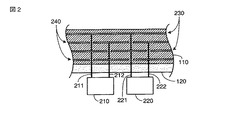
図2は、上記の集積回路における接地及びパワー面に対するデカップリングキャパシタの接続を示す線図である。図2は、デカップリングキャパシタ210及び220近傍における集積回路の小さな断面を示す。上述のように、デカップリングキャパシタ210及び220は基板120の下面上に配置される。デカップリングキャパシタ210及び220の夫々は一対のリードを有し、ここで、デカップリングキャパシタ210のためにリード211及び212が配設され、デカップリングキャパシタ220のためにリード221及び222が配設される。留意点として、これらの2本リードキャパシタは単純化のために示されており、幾つかの実施形態では、インダクタンスを減少するように、より多くの(例えば、8本または10本)リードを有する可能性がある。各デカップリングキャパシタの一方のリード(例えば、リード211及び221)は、集積回路ダイス110内のパワー面230に接続される。各デカップリングキャパシタの他方のリード(例えば、リード212及び222)は、集積回路ダイス110内の接地面240に接続される。デカップリングキャパシタによって提供される接地及びパワー面間の容量は、各DC電圧を隔離する一方で、両面間の高周波数信号(例えば、スイッチングノイズ)を分流するように機能する。
FIG. 2 is a diagram showing the connection of the decoupling capacitor to the ground and power planes in the integrated circuit. FIG. 2 shows a small cross section of the integrated circuit in the vicinity of the
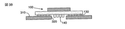
図3A−図3Cは、従来技術に係る回路基盤上の集積回路パッケージの実装を示す線図である。図3Aは、回路基盤上の集積回路パッケージの平面図である。図3Bは、回路基盤上の集積回路パッケージの断面図である。図3Cは、回路基盤内の孔を通して集積回路パッケージ及びデカップリングキャパシタの一部を示す、回路基盤の底面図である。 3A-3C are diagrams illustrating the mounting of an integrated circuit package on a circuit board according to the prior art. FIG. 3A is a plan view of an integrated circuit package on a circuit board. FIG. 3B is a cross-sectional view of an integrated circuit package on a circuit board. FIG. 3C is a bottom view of the circuit board showing a portion of the integrated circuit package and decoupling capacitor through holes in the circuit board.
図3Aに関し、集積回路パッケージ100がプリント回路基盤310上に実装される。集積回路パッケージ100の入力及び出力は、集積回路パッケージの下面上のBGAボール130を介して回路基盤上の導電性トレースに直接的に接続される。この接続は、図3Bにおいてより明確に見ることができる。
With reference to FIG. 3A, an
典型的には、BGAボール130は、デカップリングキャパシタ140と比較して小さい。例えば、BGAボールは約0.4mmの高さである一方、デカップリングキャパシタは約0.8mmの高さである可能性がある。従って、デカップリングキャパシタ140は、BGAボール130の高さだけ離間する集積回路パッケージ100及び回路基盤310間の間隙には適合しないことは明白である。従って、回路基盤310に孔320を形成することが必要である。集積回路パッケージ100が回路基盤310上に実装される時、デカップリングキャパシタ140は孔320内に延在し、その結果、回路基盤310に対する集積回路パッケージ100の接続に干渉することがない。
Typically, the
高性能マイクロプロセッサのような集積回路は、大量のパワーを消費することが典型的であるため、集積回路の動作中に生成される熱を消散するための機構を提供することがしばしば必要である。この目的のため、ヒートシンクまたはヒートスプレッダが一般的に使用される。シンクは、集積回路から熱を引き離すために使用される。ヒートスプレッダは、特定のスポットで生成される熱をより大きな領域に分散させるために使用される。通常、両機能は同じ物理的構造(例えば、集積回路と熱的にコンタクトするように配置されたフィンの付いた金属板または他の構造)によって達成されるため、本明細書においてこれら2つの区別はしない。 Because integrated circuits such as high performance microprocessors typically consume large amounts of power, it is often necessary to provide a mechanism for dissipating the heat generated during operation of the integrated circuit. . For this purpose, heat sinks or heat spreaders are commonly used. The sink is used to draw heat away from the integrated circuit. A heat spreader is used to disperse the heat generated at a particular spot over a larger area. Since both functions are usually accomplished by the same physical structure (eg, a finned metal plate or other structure placed in thermal contact with the integrated circuit), the distinction between these two is used herein. Don't do it.
図4A−図4Bは、従来技術に係る集積回路パッケージに対するヒートシンク/スプレッダの結合を示す線図である。図4Aは、回路基盤、集積回路パッケージ、及びヒートシンク/スプレッダの構成を、ヒートシンク/スプレッダに殆どまたは全く圧力が付与されていない状態で示す。図4Bは、図4Aと同じ構成を、ヒートシンク/スプレッダに圧力が付与されている状態で示す。 4A-4B are diagrams illustrating heat sink / spreader coupling to an integrated circuit package according to the prior art. FIG. 4A shows the circuit board, integrated circuit package, and heat sink / spreader configuration with little or no pressure applied to the heat sink / spreader. FIG. 4B shows the same configuration as FIG. 4A with pressure applied to the heat sink / spreader.
図4Aに関し、上述のように、集積回路パッケージ100が回路基盤310上に実装される。次に、ヒートシンク/スプレッダ410が集積回路ダイス110の上面にコンタクトして配置される。典型的には、ヒートシンク/スプレッダ410及び集積回路ダイス110のコンタクト面は、両者間に良好な熱的コンタクトが形成されるように適合する(例えば、両者とも平坦)。集積回路ダイス110からヒートシンク/スプレッダ410への熱移動を改善するため、高伝熱性を有する物質(これは、熱的仲介材料またはTIMとしても言及されるであろう)がこれらの2つの構成部品間に配置されることができる。
With reference to FIG. 4A, the
この態様で熱的に結合される2つの部品間の熱移動の効率は、典型的には、部品に圧力を付与して強制的に一体的とすることにより改良可能となる。これにより、部品間の熱的仲介材料の層の厚さが減少する。図4A−図4Bの線図において、ヒートシンク/スプレッダに対向する回路基盤310の下面に対して背板を配置することにより、ヒートシンク/スプレッダ410に対して圧力が付与される。ヒートシンク/スプレッダを集積回路ダイス110に対して押圧するように、ピンの組み合わせが、ヒートシンク/スプレッダ410及び背板430を通して配置される共に締め付けられる。しかし、回路基盤310に孔があるため、この態様でヒートシンク/スプレッダ410に圧力を付与すると、集積回路ダイス110からの熱移動の効率が実際には低下する可能性がる。何故なら、付与された圧力により、集積回路ダイス110(及び集積回路パッケージ100の残部)が、孔に向かうと共にヒートシンク/スプレッダ410から離れるように屈曲するからである。この場合、集積回路ダイス110及びヒートシンク/スプレッダ410間に間隙が形成され、熱的仲介材料の層の厚さを増加させ(または、熱的仲介材料が使用されない場合には間隙が形成され)、これにより、集積回路ダイスとヒートシンク/スプレッダとの間の熱移動が阻害される。
The efficiency of heat transfer between two parts that are thermally coupled in this manner can typically be improved by applying pressure to the parts and forcing them together. This reduces the thickness of the layer of thermal mediator material between the parts. In the diagrams of FIGS. 4A-4B, pressure is applied to the heat sink /
本発明の一実施形態において、デカップリングキャパシタは、集積回路ダイスの領域の全体に亘って均等に分布される規則正しく離間する位置ではなく、集積回路の「ホットスポット」の近傍に配置される。デカップリングキャパシタをホットスポットの近傍に配置することにより、スイッチングノイズはより効果的に減少される。更に、デカップリングキャパシタが不均等に分布される場合、デカップリングキャパシタを収容するために回路基盤に形成された孔は、集積回路の中心部分に対してサポートを提供するように形成することができる。これにより、集積回路ダイスとヒートシンク/スプレッダとの間の熱的結合の有効性を減少させる集積回路の屈曲を抑制または排除することができる。集積回路内のスイッチングノイズもまた、集積回路内の接地面及び/またはパワー面を接続するビアの濃度を高くすることにより減少される。 In one embodiment of the invention, the decoupling capacitors are located in the vicinity of the “hot spots” of the integrated circuit, rather than regularly spaced locations that are evenly distributed throughout the area of the integrated circuit die. By placing the decoupling capacitor in the vicinity of the hot spot, the switching noise is more effectively reduced. Further, if the decoupling capacitors are unevenly distributed, the holes formed in the circuit board to accommodate the decoupling capacitors can be formed to provide support for the central portion of the integrated circuit. . This can suppress or eliminate the bending of the integrated circuit that reduces the effectiveness of the thermal coupling between the integrated circuit die and the heat sink / spreader. Switching noise in the integrated circuit is also reduced by increasing the concentration of vias connecting the ground plane and / or power plane in the integrated circuit.
多くの場合、集積回路の物理的レイアウトは、通常動作中に高レベルの活動を経験する構成部品をより高い濃度で含む1つ以上の領域を有することとなる。これらの領域における高レベルの活動により、これらの領域において回路構成部品によって使用されるパワー量は、他の領域よりも高い。このため、集積回路の他の領域よりも、これらの領域において、より大量の熱が消散される。これらの領域において、より高いレベルの活動及びより大量のパワーの消散があるため、これらはしばしば「ホットスポット」として言及される。 In many cases, the physical layout of an integrated circuit will have one or more regions that contain a higher concentration of components that experience high levels of activity during normal operation. Due to the high level of activity in these areas, the amount of power used by circuit components in these areas is higher than in other areas. Thus, a greater amount of heat is dissipated in these areas than in other areas of the integrated circuit. In these areas, these are often referred to as “hot spots” because of higher levels of activity and greater dissipation of power.
図5Aは、一実施形態に係る、集積回路ダイス上のホットスポットを示す線図である。この実施形態において、集積回路ダイス510は2つのホットスポット520及び521を含む。これらは、集積回路の動作中、比較的高レベルの活動が存在するダイスの領域である。留意点として、図中に破線で概略的に示されるホットスポットは、活動及び対応する熱消散のレベルにおける明白な変化を示すものではなく、これらのレベルは、活動/熱が非常に高い領域から、活動/熱がより低い領域へ徐々に変化するものである。破線は、各ホットスポットの大凡の領域を単に指示するだけである。また留意点として、図5Aは2つのホットスポットを示すが、他の集積回路はより多くのまたはより少ないホットスポットを有する可能性があり、更にこれらのホットスポットは規則正しくまたは不規則に形作られる可能性がある。
FIG. 5A is a diagram illustrating hot spots on an integrated circuit die, according to one embodiment. In this embodiment, integrated circuit die 510 includes two
同時的スイッチングノイズを減少させるためのデカップリングキャパシタの使用に関し、デカップリングキャパシタがホットスポットまたはその近傍で集積回路に接続される方が、デカップリングキャパシタが集積回路ダイスの領域の全体に亘って均等に分布されるよりも効果的であることが測定されている。従って、規則正しいパターン(例えば、図1及び図2に示すパターン)でデカップリングキャパシタを集積回路ダイス上に配置する従来技術は、ホットスポットまたはその近傍でデカップリングキャパシタをより高い濃度で配置するパターン(例えば、図6−図8に示すパターン)と比較して、効果が低い。 With regard to the use of decoupling capacitors to reduce simultaneous switching noise, it is more uniform over the entire area of the integrated circuit die when the decoupling capacitor is connected to the integrated circuit at or near the hot spot. It has been measured to be more effective than distributed in Therefore, the conventional technique of arranging the decoupling capacitors on the integrated circuit die in a regular pattern (for example, the pattern shown in FIGS. 1 and 2) is a pattern in which the decoupling capacitors are arranged at a higher concentration at or near the hot spot ( For example, the effect is low as compared with the patterns shown in FIGS.
各ホットスポットの範囲は正確に規定できないという理由、及びデカップリングキャパシタは有限の物理的範囲を有するという理由から、デカップリングキャパシタの配置がホットスポット境界と厳密に適合することは不可能である。このため、デカップリングキャパシタの配置は、ホットスポットに関連してキャパシタの分布または濃度(単位領域あたりのキャパシタの数)として、以下に記載される。本発明の実施形態では、集積回路ダイスの領域の全体に亘って均等な分布に対応する規則正しく離間するアレイでキャパシタを配置する従来技術を採用しない。代わりに、本発明の実施形態では、集積回路ダイスの領域の全体に亘って均等でない分布に対応する不規則に離間する構成でキャパシタを配置する。デカップリングキャパシタのこの不均等分布は、ホットスポットまたはその近傍でキャパシタをより高い濃度で有すると共に、ホットスポットを含まない領域においてより低い濃度で有する。 Due to the fact that the range of each hot spot cannot be precisely defined and because the decoupling capacitor has a finite physical range, it is impossible for the decoupling capacitor placement to closely match the hot spot boundary. For this reason, the arrangement of decoupling capacitors is described below as the distribution or concentration of capacitors (number of capacitors per unit area) in relation to hot spots. Embodiments of the present invention do not employ prior art techniques in which capacitors are arranged in a regularly spaced array corresponding to an even distribution throughout the area of the integrated circuit die. Instead, in embodiments of the present invention, capacitors are arranged in an irregularly spaced configuration that corresponds to an uneven distribution throughout the area of the integrated circuit die. This non-uniform distribution of decoupling capacitors has a higher concentration of capacitors at or near hot spots and a lower concentration in regions that do not include hot spots.
図5Bは、一実施形態に係る、集積回路パッケージの下面上におけるデカップリングキャパシタ及びBGAボールコネクタの配置を示す線図である。この図は、集積回路ダイス510が実装される基板530の下面を示す。留意点として、図5Aに示す集積回路ダイス510は、図5Aにおけるダイス510の向きが図5Bの基板530上の実装位置におけるものと同じであるように、必要に応じて示される。従って、図5Bにおけるホットスポット520及び521の位置は、図5Aに示すそれと同じである。
FIG. 5B is a diagram illustrating the placement of decoupling capacitors and BGA ball connectors on the bottom surface of an integrated circuit package, according to one embodiment. This figure shows the lower surface of the
基板530の反対側における集積回路ダイス510の位置は、図5Bに破線で示される。図5A及び図5Bに示すように、デカップリングキャパシタ540がホットスポット520及び521に配置される。6個のデカップリングキャパシタの集団がホットスポット520上に配置され、4個のデカップリングキャパシタの集団がホットスポット521上に配置される。集積回路におけるスイッチング活動の多くはホットスポット520及び521で発生するため、これらのホットスポット上にデカップリングキャパシタ540を配置することにより、均等分布よりも、同時的スイッチングノイズをより効果的に減少させることができる。
The position of the integrated circuit die 510 on the opposite side of the
上述のように、各ホットスポットの範囲は正確に規定できないため、本明細書において、ホットスポット「上に」デカップリングキャパシタが配置されるということは、デカップリングキャパシタ位置とホットスポット位置との間の大凡の相関関係を示すもので、厳密な相関関係を示すものではない。ホットスポット上へのデカップリングキャパシタの配置は、代わりに、ホットスポットの領域におけるデカップリングキャパシタの濃度として言及される可能性がある。図5Bに示すように、デカップリングキャパシタの濃度は、集積回路ダイス510のホットスポットから離れた領域(例えば、集積回路ダイスの右上側コーナ)と比較して、ホットスポット520及び521の領域においてより高い。
As described above, since the range of each hot spot cannot be accurately defined, in the present specification, the decoupling capacitor is arranged “on” the hot spot between the decoupling capacitor position and the hot spot position. This is a general correlation, and not a strict correlation. The placement of the decoupling capacitor on the hot spot may instead be referred to as the concentration of the decoupling capacitor in the region of the hot spot. As shown in FIG. 5B, the concentration of the decoupling capacitor is greater in the
上述のように、集積回路ダイスのホットスポットの近傍でより高い濃度でデカップリングキャパシタを配置すると、集積回路が実装されることとなる回路基盤が、集積回路ダイスの中心部分にサポートを提供するように構成されるという更なる利点を得ることができる可能性がある。図5Bに示すように、デカップリングキャパシタ540は2つの集団に組分けされ、その1つは集積回路ダイスの左側にあり、他の1つは集積回路ダイスの右側にある。これらの2集団のデカップリングキャパシタの間に間隔をあけることにより、2組のデカップリングキャパシタの間に、一連のBGAボールを配置することが可能となる。これらのBGAボールは、集積回路パッケージが実装されることとなる回路基盤の対応する部分にコンタクトし、これによって集積回路パッケージの中心部分を支持する。
As described above, placing a decoupling capacitor at a higher concentration near the hot spot of an integrated circuit die will cause the circuit board on which the integrated circuit will be mounted to provide support to the central portion of the integrated circuit die. There is a possibility that a further advantage of being configured can be obtained. As shown in FIG. 5B, the
図5Cは、回路基盤560の下面を、そこに実装された集積回路パッケージと共に示す図である。この図においても、集積回路ダイス510の位置が破線によって示される。集積回路ダイス510の範囲に概ね適合する単一の大きな孔を有する(従来技術のように)のではなく、回路基盤560は、集積回路パッケージの下面上の2組のデカップリングキャパシタを収容するように、2つの孔570及び571を含む。この図において、デカップリングキャパシタの位置も破線によって示される。留意点として、回路基盤560は、集積回路パッケージ上の2組のデカップリングキャパシタ間に配置される、一連のBGAボールにコンタクトする部分を、孔570及び571間に含む。回路基盤560のこの部分は、集積回路パッケージの中心部分に対してサポートを提供する。
FIG. 5C is a view showing the lower surface of the
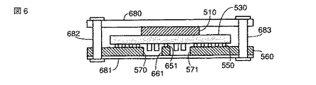
図6は、図5A−図5Cに示す集積回路パッケージ及び回路基盤の断面図である。この図において、集積回路パッケージ(集積回路ダイス510、基板530、デカップリングキャパシタ540、及びBGAボール550からなる)が、回路基盤560上に実装される。ヒートシンク/スプレッダ680が集積回路ダイス510にコンタクトして配置されると共に、ヒートシンク/スプレッダに圧力が付与される。この圧力の付与は、回路基盤560の下に裏板681を配置すると共に、ピン682及び683を使用してヒートシンク/スプレッダを裏板に接続することにより行われる。この図により明確に示されるように、孔570及び571間の回路基盤560の部分(661)が2組のデカップリングキャパシタ間で一連のBGAボール(651)にコンタクトし、集積回路パッケージの中心部分に対してサポートを提供する。その結果、ヒートシンク/スプレッダ680に圧力が付与された時、集積回路パッケージはヒートシンク/スプレッダから離れるように屈曲することができず、これにより、集積回路ダイス510及びヒートシンク/スプレッダ間に良好な熱的コンタクトが維持される。従って、ヒートシンク/スプレッダの有効性に悪影響を及ぼすことなく、デカップリングキャパシタの使用によって集積回路における同時的スイッチングノイズが減少される。
FIG. 6 is a cross-sectional view of the integrated circuit package and circuit board shown in FIGS. 5A-5C. In this figure, an integrated circuit package (consisting of an integrated circuit die 510, a
上述のように、集積回路における同時的スイッチングノイズはまた、集積回路基板の接地及びパワー面間にビアを適正に配置することにより、減少させることが可能である。典型的には、集積回路基板は複数の層を含む。各層は、種々の回路構成部品及び導電性トレースを含む可能性がある。異なる層の構成部品またはトレース間の接続は、集積回路基板内のビアによって形成することが可能である。ビアは、典型的には、集積回路基板の1つ以上の層に孔を穿つと共に、孔に半田を埋め込む(またはコーティングする)ことにより形成される電気的配線である。 As mentioned above, simultaneous switching noise in an integrated circuit can also be reduced by properly placing vias between the ground and power planes of the integrated circuit board. Typically, an integrated circuit substrate includes multiple layers. Each layer may include various circuit components and conductive traces. Connections between components or traces of different layers can be formed by vias in the integrated circuit board. A via is typically an electrical wiring formed by drilling holes in one or more layers of an integrated circuit substrate and embedding (or coating) solder in the holes.
典型的には、集積回路の各層における電気的構成部品は、パワー源及び接地接続を有する必要がある。このため、通常、各層には、ソース電圧(例えば、Vdd)に接続される多数の電気的トレースと、接地電位に接続される多数のトレースとが存在する。これを記載する目的で、層上のソース電圧電位にあるトレースがパワー面として言及される一方、層上の接地電位にあるトレースが接地面として言及される。通常、異なる層のパワー/接地面を互いに接続すると共にデカップリングキャパシタに接続するため、複数のビアが配設される。従来的には、これらのビアは、都合がよければどの位置にでも形成される。 Typically, the electrical components in each layer of an integrated circuit need to have a power source and a ground connection. Thus, typically, each layer has a number of electrical traces connected to the source voltage (eg, Vdd) and a number of traces connected to the ground potential. For the purpose of describing this, the trace at the source voltage potential on the layer is referred to as the power plane, while the trace at the ground potential on the layer is referred to as the ground plane. Typically, a plurality of vias are provided to connect the power / ground planes of different layers to each other and to connect to a decoupling capacitor. Traditionally, these vias are formed at any convenient location.
パワー面及び/または接地面に接続されるこれらのビアの存在は、同時的スイッチングノイズの減少に有益であることが測定されている。これらのビアが有益であるため、本発明の実施形態の幾つかは、更なるノイズの減少を提供するため、ビアを使用する。より具体的には、これらのビアは、集積回路内のホットスポットと関係なく適当な位置に配置されるのではなく、ホットスポットまたはその近傍でより高い濃度(即ち、単位領域あたりのビアの数が多い)でビアが存在すると共に、集積回路の他の領域においてより低い濃度でビアが存在するように配置される。 The presence of these vias connected to the power plane and / or ground plane has been measured to be beneficial in reducing simultaneous switching noise. Because these vias are beneficial, some of the embodiments of the present invention use vias to provide further noise reduction. More specifically, these vias are not placed at the proper location regardless of the hot spots in the integrated circuit, but are more concentrated at the hot spots or nearby (ie, the number of vias per unit area). The vias are present, and the vias are arranged at lower concentrations in other areas of the integrated circuit.
接地及び/またはパワー面間のビアの濃度の変化は、図7に関して例示される。この図は、対応するビアによる接地及びパワー面の相互接続を示す集積回路基板の断面図である。この図において、集積回路ダイス710が基板730上に実装される。基板730は複数の層を含み、各層は接地面及びパワー面を含む可能性がある。図7において、4個のそのような面(760-763)が示される。これらの面の2つがパワー面で、2つが接地面であるとする。例えば、面760及び762をパワー面とする一方、面761及び763を接地面とすることができる。複数のビア(例えば、770)が、パワー面760をパワー面762に接続する。同様に、複数のビアが、パワー面761をパワー面763に接続する。また、複数のビアが、接地及びパワー面をデカップリングキャパシタ780及び781に接続する。ここで、集積回路ダイスの第1の部分750がホットスポットである一方、第2の部分751がホットスポットでないとする。この図に示すように、ビアの濃度は、ホットスポットの領域(集積回路ダイスの部分750)の方が、非ホットスポットの領域(部分751)より高い。
The change in via concentration between ground and / or power plane is illustrated with respect to FIG. This figure is a cross-sectional view of an integrated circuit board showing ground and power plane interconnections with corresponding vias. In this figure, an integrated circuit die 710 is mounted on a
この図において、ビアの1つだけが参照符号770で明示されるが、この参照符号はビアを集合的に示すことを意図する。図を明確にするため、ビアの1つだけがこの参照符号によって明示される。
In this figure, only one of the vias is designated by
留意点として、デカップリングキャパシタの分布と同様に、パワー及び/または接地面を相互接続するビアの配置は、ホットスポットのあいまいな境界と厳密に対応させることはできない。従って、本明細書において、ビアが集中するということは、ホットスポットの近傍でビアの間隔が概ねより小さいということを意味すると解釈すべきである。 It should be noted that, like the distribution of decoupling capacitors, the placement of vias that interconnect power and / or ground planes cannot correspond exactly to the ambiguous boundaries of hot spots. Therefore, in this specification, the concentration of vias should be interpreted as meaning that the interval between vias is generally smaller in the vicinity of the hot spot.
以上の説明は、本発明の特定の実施形態に指向されるものである。これらの実施形態は例示することを意図し、上述の特徴の多くの変更例が代替実施形態に含まれる可能性がある。例えば、ホットスポットの位置は、異なる設計の集積回路間でかなり変更されることが予想される。これらの異なる集積回路に接続されるデカップリングキャパシタの位置もまた、従って変更される。また同様に、これらの集積回路が実装される回路基盤の構成も変更され、また、ホットスポットの位置及びデカップリングキャパシタの対応する位置も異なってくる。 The above description is directed to specific embodiments of the present invention. These embodiments are intended to be exemplary, and many variations of the features described above may be included in alternative embodiments. For example, the location of the hot spot is expected to vary considerably between different designs of integrated circuits. The position of the decoupling capacitor connected to these different integrated circuits is also changed accordingly. Similarly, the configuration of the circuit board on which these integrated circuits are mounted is changed, and the position of the hot spot and the corresponding position of the decoupling capacitor are also different.
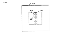
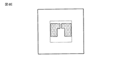
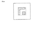
図8A−図8Hは、ホットスポット位置、デカップリングキャパシタ位置、及び回路基盤孔の可能な変更例を示す。これらの図の夫々において、外側の実線(例えば、860)は回路基盤を示す。破線の正方形(例えば、810)は集積回路ダイスの位置を示す。内側の実線(例えば、870)は回路基盤の孔を示す。小さな破線の矩形(例えば、840)はデカップリングキャパシタの位置を示す。図において、デカップリングキャパシタ及び回路基盤の対応する孔だけが示されるが、デカップリングキャパシタの位置は各集積回路のホットスポットに対応するものとする。 8A-8H show possible variations of the hot spot position, decoupling capacitor position, and circuit board hole. In each of these figures, the outer solid line (eg, 860) indicates the circuit board. A dashed square (eg, 810) indicates the location of the integrated circuit die. The inner solid line (eg, 870) indicates a circuit board hole. A small dashed rectangle (eg, 840) indicates the position of the decoupling capacitor. In the figure, only the decoupling capacitors and corresponding holes in the circuit board are shown, but the positions of the decoupling capacitors correspond to the hot spots of each integrated circuit.
図8Aは、回路基盤860に単一の孔870を有する実施形態を示す。この実施形態において、デカップリングキャパシタ840が、集積回路26の頂部からダイス810の底部へ延存する帯に集中される。孔870は狭いため、ヒートシンク/スプレッダによってパッケージに圧力が付与された時、集積回路パッケージが大幅に屈曲することはない。従って、ダイスの中心近傍の更なるサポートは不要である。図8Bは、デカップリングキャパシタが、集積回路ダイスの領域の全体に亘る帯の近傍に配設された他の実施形態を示す。ダイスの中心近傍にデカップリングキャパシタが存在しないため、ダイスの屈曲に対抗するように、回路基盤がダイスの中心部分にサポートを提供する。
FIG. 8A shows an embodiment having a
図8Cは、デカップリングキャパシタが、集積回路ダイスの両側の対称的な2集団として配置された実施形態を示す。回路基盤は、キャパシタのこれらの集団を収容する孔の間の部分を含み、集積回路パッケージの中心部分に対してサポートが提供される。図8Dは、デカップリングキャパシタの集団及び回路基盤の対応する孔が存在するが、組分けがより不規則な代替実施形態を示す。この場合も、これらの集団の間に間隔が存在するため、孔の間の回路基盤の部分によって集積回路パッケージに対してサポートが提供される。 FIG. 8C shows an embodiment in which the decoupling capacitors are arranged as two symmetrical groups on either side of the integrated circuit die. The circuit board includes portions between the holes that accommodate these populations of capacitors and provides support for the central portion of the integrated circuit package. FIG. 8D shows an alternative embodiment where there is a population of decoupling capacitors and corresponding holes in the circuit board, but the grouping is more irregular. Again, because there is a spacing between these populations, the portion of the circuit board between the holes provides support for the integrated circuit package.
図8Eは、デカップリングキャパシタが不規則ではあるが対称的な集団として配置された実施形態を示す。これらの集団の間に回路基盤の部分が残存し、集積回路ダイスの中心部分のためのサポートを提供する(2集団の間のより大きな回路基盤の部分に対して更なる安定性を提供するように、2集団のうちの近接するキャパシタの間に小さな帯を含む)。図8Fは、「C」字型構成をなすデカップリングキャパシタの単一の不規則な集団を示す。「C」字型の中心の回路基盤の部分が集積回路ダイスの中心部分に対してサポートを提供する。 FIG. 8E shows an embodiment in which the decoupling capacitors are arranged as an irregular but symmetric population. A portion of the circuit board remains between these groups, providing support for the central part of the integrated circuit die (to provide additional stability for the larger circuit board part between the two groups. And a small band between adjacent capacitors of the two populations). FIG. 8F shows a single irregular group of decoupling capacitors in a “C” shaped configuration. The “C” -shaped central circuit board portion provides support for the central portion of the integrated circuit die.
図8Gは、3集団のデカップリングキャパシタが存在する実施形態を示す。留意点として、異なる集積回路において、ホットスポットは、位置だけでなく数も変わる可能性がある。デカップリングキャパシタのより大きな組分けの間に回路基盤の部分が残存し、集積回路ダイスに対してサポートを提供する。図8Hは、2集団のデカップリングキャパシタが存在する実施形態を示す。この実施形態において、集積回路ダイスの右下側コーナの集団のデカップリングキャパシタは、残りのデカップリングキャパシタよりも小さい間隔で配置される。留意点として、種々の実施形態は、各集積回路のホットスポットまたはその近傍でない位置に配置されるデカップリングキャパシタを含む可能性がある。デカップリングキャパシタの配置はホットスポットだけに限定される必要はないが、これらの領域でより高い濃度となっている必要がある。図8Hの実施形態においても、集積回路ダイスの中心部分に対してサポートを提供する回路基盤の部分が存在する。 FIG. 8G shows an embodiment where there are three groups of decoupling capacitors. It should be noted that in different integrated circuits hot spots can vary not only in position but also in number. The portion of the circuit board remains during the larger grouping of decoupling capacitors, providing support for the integrated circuit die. FIG. 8H shows an embodiment where there are two populations of decoupling capacitors. In this embodiment, the decoupling capacitors of the group of lower right corners of the integrated circuit die are arranged at a smaller spacing than the remaining decoupling capacitors. It should be noted that various embodiments may include a decoupling capacitor located at a location that is not at or near the hot spot of each integrated circuit. The arrangement of the decoupling capacitor need not be limited to hot spots, but needs to be higher in these areas. Also in the embodiment of FIG. 8H, there is a portion of the circuit board that provides support for the central portion of the integrated circuit die.
当業者は更に、ここで開示した実施形態に関して説明した種々の例示的な論理ブロック、モジュール、及び演算ステップが、種々の態様で実施可能であることを認識するであろう。以上では、この互換性を明白に示すため、種々の例示的な構成部品、ブロック、モジュール、及びステップが、それらの機能に関して概略的に記載される。当業者は各特定の応用に対して、記載された機能を種々の態様で実施するであろうが、そのような実施上の決定は本発明の技術的範囲から離れるものと解釈されるべきではない。 Those skilled in the art will further appreciate that the various exemplary logic blocks, modules, and operational steps described with respect to the embodiments disclosed herein can be implemented in various ways. In the foregoing description, various illustrative components, blocks, modules, and steps are schematically described with respect to their functionality in order to demonstrate this interchangeability. Those skilled in the art will implement the described functions in various ways for each particular application, but such implementation decisions should not be construed as departing from the scope of the invention. Absent.
以上では、本発明により与えられる効果及び利点が特定の実施形態に関して説明される。これらの効果及び利点、ならびに、これらを発生またはより明白にするいかなるエレメントまたは限定も、特許請求の範囲に記載の請求項のいずれかまたは全てについての、臨界的な、必要な、または基本的な特徴として解釈されるべきではない。ここで使用されるように、用語「具備する」、「具備している」または任意の他のその変更例は排他的ではなく、これらの用語に付随する要件または限定を含むものとして解釈されることを意図する。従って、1組の要件を含むシステム、方法、またはその他の実施形態は、これらの要件だけに限定されることを意図するものではなく、記載されていない或いは請求された実施形態に固有ではないその他の要件を含むことができる。 In the foregoing, the advantages and benefits afforded by the present invention are described with respect to particular embodiments. These effects and advantages, as well as any elements or limitations that may cause or make them more obvious, are critical, necessary, or fundamental for any or all of the claims recited in the claims. It should not be interpreted as a feature. As used herein, the terms “comprising”, “comprising” or any other modifications thereof are not exclusive and are to be interpreted as including the requirements or limitations associated with these terms. I intend to. Accordingly, a system, method, or other embodiment that includes a set of requirements is not intended to be limited only to those requirements, but is not described or otherwise unique to the claimed embodiment Requirements can be included.
開示される実施形態の以上の説明は、当業者が本発明を実行または使用可能にするために提供される。これらの実施形態に対する種々の変形は当業者にとって容易に明白であり、ここで規定される一般原理は本発明の技術的範囲を逸脱せずに他の実施形態に適用されることができる。従って、本発明はここで示された実施形態に限定されず、ここで説明され且つ特許請求の範囲で列挙される原理及び新規な特徴と一貫して最も広い範囲に従うことを意図する。 The previous description of the disclosed embodiments is provided to enable any person skilled in the art to make or use the present invention. Various modifications to these embodiments will be readily apparent to those skilled in the art, and the generic principles defined herein may be applied to other embodiments without departing from the scope of the invention. Accordingly, the present invention is not intended to be limited to the embodiments shown herein but is to be accorded the widest scope consistently with the principles and novel features described herein and recited in the claims.
本発明によれば、例えば、以下の視点1乃至20に記載されるようなデバイス及び方法が提供可能である。 According to the present invention, for example, devices and methods as described in the following viewpoints 1 to 20 can be provided.
[視点1]
集積回路と、
前記集積回路に外部的に接続された1つ以上のデカップリングキャパシタと、
を具備し、前記デカップリングキャパシタは、前記集積回路内の1つ以上のホットスポットにおいてより高い濃度となるように配置されるデバイス。
[Viewpoint 1]
An integrated circuit;
One or more decoupling capacitors externally connected to the integrated circuit;
And wherein the decoupling capacitor is arranged to have a higher concentration at one or more hot spots in the integrated circuit.
[視点2]
視点1のデバイスにおいて、前記デカップリングキャパシタは、前記集積回路に対して不規則な間隔をあけて配置される。
[Viewpoint 2]
In the device of viewpoint 1, the decoupling capacitors are arranged at irregular intervals with respect to the integrated circuit.
[視点3]
視点1のデバイスにおいて、前記デカップリングキャパシタは、集積回路ダイスが実装される基板を通して前記集積回路に接続され、前記基板は、前記集積回路ダイスのための1つ以上のコネクタを含む。
[Viewpoint 3]
In the device of viewpoint 1, the decoupling capacitor is connected to the integrated circuit through a substrate on which an integrated circuit die is mounted, and the substrate includes one or more connectors for the integrated circuit die.
[視点4]
視点3のデバイスにおいて、1つ以上の孔が形成された回路基盤を更に具備し、前記孔は、前記基板が前記回路基盤に実装される時、前記デカップリングキャパシタが前記孔を通して延存するように配置される。
[Viewpoint 4]
The device of aspect 3 further comprises a circuit board having one or more holes formed therein, such that the decoupling capacitor extends through the holes when the substrate is mounted on the circuit board. Be placed.
[視点5]
視点4のデバイスにおいて、前記デカップリングキャパシタ及び前記孔は、前記集積回路に対して非対称的に配置される。
[Viewpoint 5]
In the device of viewpoint 4, the decoupling capacitor and the hole are arranged asymmetrically with respect to the integrated circuit.
[視点6]
視点4のデバイスにおいて、前記回路基盤は、前記集積回路の中心部分の下側に配置された部分を含む。
[Viewpoint 6]
In the device of the viewpoint 4, the circuit board includes a portion disposed below a central portion of the integrated circuit.
[視点7]
視点6のデバイスにおいて、前記集積回路の前記中心部分の下側に配置された前記回路基盤の部分は、前記基板上の前記コネクタの1つ以上にコンタクトする。
[Viewpoint 7]
In the device of point of view 6, a portion of the circuit board disposed below the central portion of the integrated circuit contacts one or more of the connectors on the substrate.
[視点8]
視点7のデバイスにおいて、
前記集積回路ダイスに熱的コンタクトを形成するように配置されるヒートシンク/スプレッダと、
前記集積回路ダイスとの前記熱的コンタクトを維持するように、前記ヒートシンク/スプレッダに対して圧力を付与するように構成されたカップリングと、
を更に具備する。
[Viewpoint 8]
In the device of viewpoint 7,
A heat sink / spreader arranged to form a thermal contact to the integrated circuit die;
A coupling configured to apply pressure to the heat sink / spreader to maintain the thermal contact with the integrated circuit die;
Is further provided.
[視点9]
視点1のデバイスにおいて、前記集積回路は複数のビアを含み、前記ビアの第1の組は集積回路基板の2つ以上の接地面に接続されると共に、前記ビアの第2の組は前記集積回路基板の2つ以上のパワー面に接続され、前記ホットスポットの近傍における前記ビアの濃度は、前記ホットスポットの近傍でない領域における前記ビアの濃度より高い。
[Viewpoint 9]
In the viewpoint 1, the integrated circuit includes a plurality of vias, the first set of vias being connected to two or more ground planes of the integrated circuit substrate, and the second set of vias is the integrated circuit. The via concentration in the vicinity of the hot spot connected to two or more power planes of the circuit board is higher than the concentration of the via in a region not in the vicinity of the hot spot.
[視点10]
集積回路が実装されるように構成された回路基盤を具備するデバイスであって、
前記回路基盤には1つ以上の孔が形成され、前記孔は、1つ以上のデカップリングキャパシタが前記孔を通して前記集積回路に接続されるように配置され、
前記回路基盤は、前記1つ以上の孔に隣接して、前記集積回路の中心部分を支持するように配置された部分を含む。
[Viewpoint 10]
A device comprising a circuit board configured to be mounted with an integrated circuit,
One or more holes are formed in the circuit board, and the holes are arranged such that one or more decoupling capacitors are connected to the integrated circuit through the holes;
The circuit board includes a portion disposed adjacent to the one or more holes to support a central portion of the integrated circuit.
[視点11]
集積回路を提供する工程と、
前記集積回路内の1つ以上のホットスポットでより高い濃度となるように1つ以上のデカップリングキャパシタを配置する工程と、
前記デカップリングキャパシタを前記集積回路内のパワー及び/または接地面に接続する工程と、
を具備する方法。
[Viewpoint 11]
Providing an integrated circuit;
Disposing one or more decoupling capacitors to have a higher concentration at one or more hot spots in the integrated circuit;
Connecting the decoupling capacitor to a power and / or ground plane in the integrated circuit;
A method comprising:
[視点12]
視点11の方法において、前記デカップリングキャパシタは、前記集積回路に対して不規則な間隔をあけて配置される工程を更に具備する。
[Viewpoint 12]
In the method of aspect 11, the decoupling capacitor further comprises a step of being arranged at irregular intervals with respect to the integrated circuit.
[視点13]
視点11の方法において、前記デカップリングキャパシタを前記集積回路内のパワー及び/または接地面に接続する工程は、前記デカップリングキャパシタを、集積回路ダイスが実装される基板を通して前記集積回路に接続する工程を具備し、前記基板は、前記集積回路のための1つ以上のコネクタを含む。
[Viewpoint 13]
In the method of aspect 11, the step of connecting the decoupling capacitor to a power and / or ground plane in the integrated circuit includes connecting the decoupling capacitor to the integrated circuit through a substrate on which an integrated circuit die is mounted. And the substrate includes one or more connectors for the integrated circuit.
[視点14]
視点13の方法において、回路基盤を提供する工程と、前記回路基盤に1つ以上の孔を形成する工程と、を更に具備し、前記孔は、前記基板が前記回路基盤に実装される時、前記デカップリングキャパシタが前記孔を通して延存するように配置される。
[Viewpoint 14]
The method of aspect 13, further comprising: providing a circuit board; and forming one or more holes in the circuit board, wherein the holes are mounted on the circuit board when the substrate is mounted on the circuit board. The decoupling capacitor is arranged to extend through the hole.
[視点15]
視点14の方法において、前記回路基盤に前記基板を実装する工程を更に具備する。
[Viewpoint 15]
The method of the viewpoint 14 further includes a step of mounting the substrate on the circuit board.
[視点16]
視点14の方法において、前記デカップリングキャパシタ及び前記孔を、前記集積回路に対して非対称的に配置する工程を更に具備する。
[Viewpoint 16]
The method of aspect 14 further comprises the step of asymmetrically disposing the decoupling capacitor and the hole with respect to the integrated circuit.
[視点17]
視点14の方法において、前記回路基盤に孔を形成する工程は、前記集積回路の中心部分の下側に配置された部分を前記回路基盤に提供する工程を具備する。
[Viewpoint 17]
In the method of the fourteenth aspect, the step of forming a hole in the circuit board includes the step of providing the circuit board with a portion disposed below a central portion of the integrated circuit.
[視点18]
視点17の方法において、前記基板上の前記コネクタの1つ以上を、前記集積回路の前記中心部分の下側に配置された前記回路基盤の部分にコンタクトするように配置する工程を更に具備する。
[Viewpoint 18]
The method of aspect 17 further comprises the step of placing one or more of the connectors on the substrate in contact with a portion of the circuit board disposed below the central portion of the integrated circuit.
[視点19]
視点18の方法において、
前記集積回路ダイスに熱的コンタクトを形成するようにヒートシンク/スプレッダを配置する工程と、
前記集積回路ダイスとの前記熱的コンタクトを維持するように、前記ヒートシンク/スプレッダに対して圧力を付与する工程と、
を更に具備する。
[Viewpoint 19]
In the method of
Placing a heat sink / spreader to form a thermal contact to the integrated circuit die; and
Applying pressure to the heat sink / spreader to maintain the thermal contact with the integrated circuit die; and
Is further provided.
[視点20]
視点11の方法において、前記集積回路に複数のビアを形成する工程を更に具備し、前記ビアの第1の組は集積回路基板の2つ以上の接地面に接続されると共に、前記ビアの第2の組は前記集積回路基板の2つ以上のパワー面に接続され、前記ホットスポットの近傍における前記ビアの濃度は、前記ホットスポットの近傍でない領域における前記ビアの濃度より高い。
[Viewpoint 20]
The method of aspect 11 further comprises the step of forming a plurality of vias in the integrated circuit, wherein the first set of vias is connected to two or more ground planes of the integrated circuit substrate, and the first of the vias is connected. Two sets are connected to two or more power planes of the integrated circuit board, and the concentration of the via in the vicinity of the hot spot is higher than the concentration of the via in a region not in the vicinity of the hot spot.
Claims (20)
前記集積回路に外部的に接続された1つ以上のデカップリングキャパシタと、
を具備し、前記デカップリングキャパシタは、前記集積回路内の1つ以上のホットスポットにおいてより高い濃度となるように配置されるデバイス。 An integrated circuit;
One or more decoupling capacitors externally connected to the integrated circuit;
And wherein the decoupling capacitor is arranged to have a higher concentration at one or more hot spots in the integrated circuit.
前記集積回路ダイスに熱的コンタクトを形成するように配置されるヒートシンク/スプレッダと、
前記集積回路ダイスとの前記熱的コンタクトを維持するように、前記ヒートシンク/スプレッダに対して圧力を付与するように構成されたカップリングと、
を更に具備する。 The device of claim 7, wherein
A heat sink / spreader arranged to form a thermal contact to the integrated circuit die;
A coupling configured to apply pressure to the heat sink / spreader to maintain the thermal contact with the integrated circuit die;
Is further provided.
前記回路基盤には1つ以上の孔が形成され、前記孔は、1つ以上のデカップリングキャパシタが前記孔を通して前記集積回路に接続されるように配置され、
前記回路基盤は、前記1つ以上の孔に隣接して、前記集積回路の中心部分を支持するように配置された部分を含む。 A device comprising a circuit board configured to be mounted with an integrated circuit,
One or more holes are formed in the circuit board, and the holes are arranged such that one or more decoupling capacitors are connected to the integrated circuit through the holes;
The circuit board includes a portion disposed adjacent to the one or more holes to support a central portion of the integrated circuit.
前記集積回路内の1つ以上のホットスポットでより高い濃度となるように1つ以上のデカップリングキャパシタを配置する工程と、
前記デカップリングキャパシタを前記集積回路内のパワー及び/または接地面に接続する工程と、
を具備する方法。 Providing an integrated circuit;
Disposing one or more decoupling capacitors to have a higher concentration at one or more hot spots in the integrated circuit;
Connecting the decoupling capacitor to a power and / or ground plane in the integrated circuit;
A method comprising:
前記集積回路ダイスに熱的コンタクトを形成するようにヒートシンク/スプレッダを配置する工程と、
前記集積回路ダイスとの前記熱的コンタクトを維持するように、前記ヒートシンク/スプレッダに対して圧力を付与する工程と、
を更に具備する。 The method of claim 18, wherein
Placing a heat sink / spreader to form a thermal contact to the integrated circuit die; and
Applying pressure to the heat sink / spreader to maintain the thermal contact with the integrated circuit die; and
Is further provided.
12. The method of claim 11, further comprising forming a plurality of vias in the integrated circuit, the first set of vias being connected to two or more ground planes of the integrated circuit substrate, and The second set is connected to two or more power planes of the integrated circuit board, and the via concentration in the vicinity of the hot spot is higher than the via concentration in a region not in the vicinity of the hot spot.
Applications Claiming Priority (2)
| Application Number | Priority Date | Filing Date | Title |
|---|---|---|---|
| US11/105,113 US7492570B2 (en) | 2005-04-13 | 2005-04-13 | Systems and methods for reducing simultaneous switching noise in an integrated circuit |
| US11/105,113 | 2005-04-13 |
Publications (2)
| Publication Number | Publication Date |
|---|---|
| JP2006295193A true JP2006295193A (en) | 2006-10-26 |
| JP4728865B2 JP4728865B2 (en) | 2011-07-20 |
Family
ID=37107726
Family Applications (1)
| Application Number | Title | Priority Date | Filing Date |
|---|---|---|---|
| JP2006110403A Expired - Fee Related JP4728865B2 (en) | 2005-04-13 | 2006-04-13 | System and method for reducing simultaneous switching noise in integrated circuits |
Country Status (3)
| Country | Link |
|---|---|
| US (1) | US7492570B2 (en) |
| JP (1) | JP4728865B2 (en) |
| CN (1) | CN100505243C (en) |
Cited By (1)
| Publication number | Priority date | Publication date | Assignee | Title |
|---|---|---|---|---|
| JP2011138959A (en) * | 2009-12-28 | 2011-07-14 | Toshiba Corp | Electronic apparatus |
Families Citing this family (11)
| Publication number | Priority date | Publication date | Assignee | Title |
|---|---|---|---|---|
| JP5259945B2 (en) * | 2006-10-30 | 2013-08-07 | スリーエム イノベイティブ プロパティズ カンパニー | IC socket with heat dissipation function |
| WO2008099856A1 (en) * | 2007-02-15 | 2008-08-21 | Nec Corporation | Elecric device-installed apparatus and its noise reduction method |
| US8627261B1 (en) * | 2011-09-14 | 2014-01-07 | Altera Corporation | Method and apparatus for performing automatic decoupling capacitor selection for power distribution networks |
| US8739097B2 (en) * | 2012-09-14 | 2014-05-27 | Taiwan Semiconductor Manufacturing Company, Ltd. | Method for placing decoupling capacitors |
| US9967969B2 (en) * | 2014-04-21 | 2018-05-08 | Hitachi, Ltd. | Multilayer printed circuit board with switching power supply capacitors, broad patterns, and TT-type filter |
| WO2018182643A1 (en) * | 2017-03-30 | 2018-10-04 | Intel Corporation | Three-dimensional decoupling integration within hole in motherboard |
| US20200373224A1 (en) * | 2019-05-21 | 2020-11-26 | Microsoft Technology Licensing, Llc | Through-silicon vias and decoupling capacitance |
| US11158566B2 (en) * | 2019-05-24 | 2021-10-26 | Google Llc | Integrated circuit with a ring-shaped hot spot area and multidirectional cooling |
| US11710726B2 (en) | 2019-06-25 | 2023-07-25 | Microsoft Technology Licensing, Llc | Through-board power control arrangements for integrated circuit devices |
| CN112203419A (en) * | 2020-11-09 | 2021-01-08 | 徐州科亚机电有限公司 | Power circuit board for electric vehicle controller for enhancing current carrying capacity of circuit board |
| TWI898767B (en) * | 2024-08-07 | 2025-09-21 | 崑山科技大學 | Design method for the layout of output capacitors in a switch-mode power supply with constant current output |
Family Cites Families (10)
| Publication number | Priority date | Publication date | Assignee | Title |
|---|---|---|---|---|
| US5103283A (en) * | 1989-01-17 | 1992-04-07 | Hite Larry R | Packaged integrated circuit with in-cavity decoupling capacitors |
| US5272590A (en) * | 1990-02-12 | 1993-12-21 | Hernandez Jorge M | Integrated circuit package having an internal cavity for incorporating decoupling capacitor |
| US5694297A (en) * | 1995-09-05 | 1997-12-02 | Astec International Limited | Integrated circuit mounting structure including a switching power supply |
| US5956576A (en) * | 1996-09-13 | 1999-09-21 | International Business Machines Corporation | Enhanced protection of semiconductors with dual surface seal |
| US6430058B1 (en) * | 1999-12-02 | 2002-08-06 | Intel Corporation | Integrated circuit package |
| US6446317B1 (en) * | 2000-03-31 | 2002-09-10 | Intel Corporation | Hybrid capacitor and method of fabrication therefor |
| US6611419B1 (en) * | 2000-07-31 | 2003-08-26 | Intel Corporation | Electronic assembly comprising substrate with embedded capacitors |
| US6979894B1 (en) * | 2001-09-27 | 2005-12-27 | Marvell International Ltd. | Integrated chip package having intermediate substrate |
| US7173329B2 (en) * | 2001-09-28 | 2007-02-06 | Intel Corporation | Package stiffener |
| US6967416B2 (en) * | 2002-07-11 | 2005-11-22 | International Business Machines Corporation | Shared on-chip decoupling capacitor and heat-sink devices |
-
2005
- 2005-04-13 US US11/105,113 patent/US7492570B2/en not_active Expired - Fee Related
-
2006
- 2006-04-13 JP JP2006110403A patent/JP4728865B2/en not_active Expired - Fee Related
- 2006-04-13 CN CN200610073630.7A patent/CN100505243C/en not_active Expired - Fee Related
Cited By (1)
| Publication number | Priority date | Publication date | Assignee | Title |
|---|---|---|---|---|
| JP2011138959A (en) * | 2009-12-28 | 2011-07-14 | Toshiba Corp | Electronic apparatus |
Also Published As
| Publication number | Publication date |
|---|---|
| US7492570B2 (en) | 2009-02-17 |
| CN100505243C (en) | 2009-06-24 |
| CN1855475A (en) | 2006-11-01 |
| JP4728865B2 (en) | 2011-07-20 |
| US20060231947A1 (en) | 2006-10-19 |
Similar Documents
| Publication | Publication Date | Title |
|---|---|---|
| US6515870B1 (en) | Package integrated faraday cage to reduce electromagnetic emissions from an integrated circuit | |
| US5390078A (en) | Apparatus for using an active circuit board as a heat sink | |
| US8737073B2 (en) | Systems and methods providing thermal spreading for an LED module | |
| US7630202B2 (en) | High density module having at least two substrates and at least one thermally conductive layer therebetween | |
| DE69829536T2 (en) | Thermally conductive substrate press-mounted in an opening of a PC board to transfer heat from the IC to a heat sink | |
| KR100458832B1 (en) | Leadless chip carrier design and structure | |
| JP4728865B2 (en) | System and method for reducing simultaneous switching noise in integrated circuits | |
| US6480014B1 (en) | High density, high frequency memory chip modules having thermal management structures | |
| US20040218367A1 (en) | Function module with built-in heat dissipation fin | |
| CN104010432B (en) | printed circuit board structure with heat dissipation function | |
| US7042084B2 (en) | Semiconductor package with integrated heat spreader attached to a thermally conductive substrate core | |
| US6948943B2 (en) | Shunting arrangements to reduce high currents in grid array connectors | |
| KR20130077841A (en) | Set-top box having dissipating thermal loads | |
| TWI747356B (en) | Electronic module | |
| US6956285B2 (en) | EMI grounding pins for CPU/ASIC chips | |
| CN107708286B (en) | Printed circuit board assembly | |
| JP2004071670A (en) | IC package, connection structure, and electronic device | |
| KR20140073522A (en) | Method and apparatus for connecting inlaid chip into printed circuit board | |
| CN1327519C (en) | Device package, a printed wiring board, and an electronic apparatus | |
| US5362985A (en) | Packaged integrated circuit add-on card and method of manufacture | |
| US9484280B2 (en) | Semiconductor device and method of manufacturing a semiconductor device | |
| US7190056B2 (en) | Thermally enhanced component interposer: finger and net structures | |
| CN210928128U (en) | Heat sink for circuit module and circuit module | |
| JP2000020168A (en) | Information processing apparatus, component arrangement method thereof, and heat sink | |
| KR20150002127A (en) | Printed circuit board |
Legal Events
| Date | Code | Title | Description |
|---|---|---|---|
| A977 | Report on retrieval |
Free format text: JAPANESE INTERMEDIATE CODE: A971007 Effective date: 20080212 |
|
| A131 | Notification of reasons for refusal |
Free format text: JAPANESE INTERMEDIATE CODE: A131 Effective date: 20080219 |
|
| A521 | Request for written amendment filed |
Free format text: JAPANESE INTERMEDIATE CODE: A523 Effective date: 20080519 |
|
| A02 | Decision of refusal |
Free format text: JAPANESE INTERMEDIATE CODE: A02 Effective date: 20090602 |
|
| A521 | Request for written amendment filed |
Free format text: JAPANESE INTERMEDIATE CODE: A523 Effective date: 20090925 |
|
| A521 | Request for written amendment filed |
Free format text: JAPANESE INTERMEDIATE CODE: A821 Effective date: 20090928 |
|
| A911 | Transfer to examiner for re-examination before appeal (zenchi) |
Free format text: JAPANESE INTERMEDIATE CODE: A911 Effective date: 20091027 |
|
| A912 | Re-examination (zenchi) completed and case transferred to appeal board |
Free format text: JAPANESE INTERMEDIATE CODE: A912 Effective date: 20100514 |
|
| A61 | First payment of annual fees (during grant procedure) |
Free format text: JAPANESE INTERMEDIATE CODE: A61 Effective date: 20110415 |
|
| R150 | Certificate of patent or registration of utility model |
Free format text: JAPANESE INTERMEDIATE CODE: R150 |
|
| FPAY | Renewal fee payment (event date is renewal date of database) |
Free format text: PAYMENT UNTIL: 20140422 Year of fee payment: 3 |
|
| LAPS | Cancellation because of no payment of annual fees |