JP2006295343A - スイッチトキャパシタフィルタ及びフィードバックシステム - Google Patents
スイッチトキャパシタフィルタ及びフィードバックシステム Download PDFInfo
- Publication number
- JP2006295343A JP2006295343A JP2005110272A JP2005110272A JP2006295343A JP 2006295343 A JP2006295343 A JP 2006295343A JP 2005110272 A JP2005110272 A JP 2005110272A JP 2005110272 A JP2005110272 A JP 2005110272A JP 2006295343 A JP2006295343 A JP 2006295343A
- Authority
- JP
- Japan
- Prior art keywords
- capacitor
- filter
- switched capacitor
- voltage
- circuit
- Prior art date
- Legal status (The legal status is an assumption and is not a legal conclusion. Google has not performed a legal analysis and makes no representation as to the accuracy of the status listed.)
- Pending
Links
Images






Classifications
-
- H—ELECTRICITY
- H03—ELECTRONIC CIRCUITRY
- H03H—IMPEDANCE NETWORKS, e.g. RESONANT CIRCUITS; RESONATORS
- H03H19/00—Networks using time-varying elements, e.g. N-path filters
- H03H19/004—Switched capacitor networks
-
- H—ELECTRICITY
- H03—ELECTRONIC CIRCUITRY
- H03D—DEMODULATION OR TRANSFERENCE OF MODULATION FROM ONE CARRIER TO ANOTHER
- H03D13/00—Circuits for comparing the phase or frequency of two mutually-independent oscillations
- H03D13/003—Circuits for comparing the phase or frequency of two mutually-independent oscillations in which both oscillations are converted by logic means into pulses which are applied to filtering or integrating means
- H03D13/004—Circuits for comparing the phase or frequency of two mutually-independent oscillations in which both oscillations are converted by logic means into pulses which are applied to filtering or integrating means the logic means delivering pulses at more than one terminal, e.g. up and down pulses
-
- H—ELECTRICITY
- H03—ELECTRONIC CIRCUITRY
- H03L—AUTOMATIC CONTROL, STARTING, SYNCHRONISATION OR STABILISATION OF GENERATORS OF ELECTRONIC OSCILLATIONS OR PULSES
- H03L7/00—Automatic control of frequency or phase; Synchronisation
- H03L7/06—Automatic control of frequency or phase; Synchronisation using a reference signal applied to a frequency- or phase-locked loop
- H03L7/08—Details of the phase-locked loop
- H03L7/085—Details of the phase-locked loop concerning mainly the frequency- or phase-detection arrangement including the filtering or amplification of its output signal
- H03L7/089—Details of the phase-locked loop concerning mainly the frequency- or phase-detection arrangement including the filtering or amplification of its output signal the phase or frequency detector generating up-down pulses
- H03L7/0891—Details of the phase-locked loop concerning mainly the frequency- or phase-detection arrangement including the filtering or amplification of its output signal the phase or frequency detector generating up-down pulses the up-down pulses controlling source and sink current generators, e.g. a charge pump
-
- H—ELECTRICITY
- H03—ELECTRONIC CIRCUITRY
- H03L—AUTOMATIC CONTROL, STARTING, SYNCHRONISATION OR STABILISATION OF GENERATORS OF ELECTRONIC OSCILLATIONS OR PULSES
- H03L7/00—Automatic control of frequency or phase; Synchronisation
- H03L7/06—Automatic control of frequency or phase; Synchronisation using a reference signal applied to a frequency- or phase-locked loop
- H03L7/08—Details of the phase-locked loop
- H03L7/085—Details of the phase-locked loop concerning mainly the frequency- or phase-detection arrangement including the filtering or amplification of its output signal
- H03L7/093—Details of the phase-locked loop concerning mainly the frequency- or phase-detection arrangement including the filtering or amplification of its output signal using special filtering or amplification characteristics in the loop
-
- H—ELECTRICITY
- H03—ELECTRONIC CIRCUITRY
- H03L—AUTOMATIC CONTROL, STARTING, SYNCHRONISATION OR STABILISATION OF GENERATORS OF ELECTRONIC OSCILLATIONS OR PULSES
- H03L7/00—Automatic control of frequency or phase; Synchronisation
- H03L7/06—Automatic control of frequency or phase; Synchronisation using a reference signal applied to a frequency- or phase-locked loop
- H03L7/16—Indirect frequency synthesis, i.e. generating a desired one of a number of predetermined frequencies using a frequency- or phase-locked loop
- H03L7/18—Indirect frequency synthesis, i.e. generating a desired one of a number of predetermined frequencies using a frequency- or phase-locked loop using a frequency divider or counter in the loop
Landscapes
- Engineering & Computer Science (AREA)
- Power Engineering (AREA)
- Stabilization Of Oscillater, Synchronisation, Frequency Synthesizers (AREA)
- Filters That Use Time-Delay Elements (AREA)
Abstract
【解決手段】スイッチトキャパシタフィルタは、3個のスイッチトキャパシタ回路(32)を備えている。各スイッチトキャパシタ回路(32)は、容量(321)を有し、容量(321)が電流信号の入力端に接続された第1の状態、容量(321)が電圧信号の出力端に接続された第2の状態、及び容量(321)がフィルタ容量(31)の側に接続された第3の状態が循環する。そして、これら3個のスイッチトキャパシタ回路(32)は、互いに第1から第3の状態が重ならないようにインターリーブ制御される。
【選択図】図4
Description
T.Lee and B.Razavi, "A stabilization technique for phase-locked frequency synthesizer", in Proc. 2001 Symp. VLSI Circuits, Kyoto, Japan, June 2001, pp.39-42
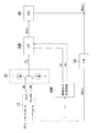
図1は、本発明の第1の実施形態に係るPLLの構成を示す。本実施形態に係るPLLは、位相比較器10と、チャージポンプ回路20と、ループフィルタ(LPF)30Aと、出力クロック生成回路としての電圧制御発振器(VCO)40と、分周器50と、制御クロック生成回路60Aとを備えている。位相比較器10は、PLLに与えられる入力クロックCKinと帰還クロックCKdivとの位相を比較し、この位相差に応じたアップ信号UPおよびダウン信号DNを出力する。チャージポンプ回路20は、アップ信号UPおよびダウン信号DNに基づいてプッシュプル動作をし、チャージ電流Ipを出力(吐き出し又は吸い込み)する。電圧制御発振器40は、ループフィルタ30Aから出力された電圧Voutに基づいて、PLLの出力クロックCKoutの周波数を変化させる。分周器50は、出力クロックCKoutをN(Nは自然数)分周し、帰還クロックCKdivとして位相比較器10にフィードバックする。以上の動作を繰り返すうちに、出力クロックCKoutは次第に所定の周波数に収束し、ロックされる。以下、ループフィルタ30A及び制御クロック生成回路60Aの構成及び動作について詳細に説明する。
図7は、本発明の第2の実施形態に係るPLLの構成を示す。本実施形態に係るPLLは、第1の実施形態に係るPLLとは異なる構成のループフィルタ30Bと、制御クロック生成回路60Bとを備えている。これ以外の構成要素については第1の実施形態と同様である。以下、第1の実施形態と異なる点についてのみ説明する。
30A、30B ループフィルタ
31 フィルタ容量
32 スイッチトキャパシタ回路(第1、第2及び第3のスイッチトキャパシタ回路)
32a スイッチトキャパシタ回路(第1のスイッチトキャパシタ回路)
32b スイッチトキャパシタ回路(第2のスイッチトキャパシタ回路)
321、321a、321b 容量
40 電圧制御発振器(出力クロック生成回路)
60A、60B 制御クロック生成回路
Claims (8)
- フィルタ容量を備え、入力された電流信号を当該フィルタ容量で平滑化して電圧信号を出力するスイッチトキャパシタフィルタであって、
ある位相で、前記電流信号の入力によって供給される電荷を充電し、次の位相で、前記充電によって生じた電圧と前の位相における前記フィルタ容量の電圧とを平均化した電圧を前記電圧信号として出力し、さらに次の位相で、前記平均化された電圧と前記フィルタ容量の電圧とをさらに平均化する
ことを特徴とするスイッチトキャパシタフィルタ。 - 請求項1に記載のスイッチトキャパシタフィルタにおいて、
容量を有し、当該容量が前記電流信号の入力端に接続された第1の状態、当該容量が前記電圧信号の出力端に接続された第2の状態、及び当該容量が前記フィルタ容量の側に接続された第3の状態が循環する第1、第2及び第3のスイッチトキャパシタ回路を備え、
前記第1から第3のスイッチトキャパシタ回路は、互いに前記第1から第3の状態が重ならないようにインターリーブ制御される
ことを特徴とするスイッチトキャパシタフィルタ。 - 請求項2に記載のスイッチトキャパシタフィルタにおいて、
前記フィルタ容量及び前記第1から第3のスイッチトキャパシタ回路における容量は、いずれもMOS容量である
ことを特徴とするスイッチトキャパシタフィルタ。 - 請求項1に記載のスイッチトキャパシタフィルタにおいて、
2個の容量を有し、いずれか一方の容量が前記電流信号の入力端に接続されるとき他の容量が前記電圧信号の出力端に接続される第1のスイッチトキャパシタ回路と、
2個の容量を有し、いずれか一方の容量が前記電圧信号の出力端に接続されるとき他の容量が前記フィルタ容量の側に接続される第2のスイッチトキャパシタ回路とを備えた
ことを特徴とするスイッチトキャパシタフィルタ。 - 請求項4に記載のスイッチトキャパシタフィルタにおいて、
前記フィルタ容量及び前記第1及び第2のスイッチトキャパシタ回路における容量は、いずれもMOS容量である
ことを特徴とするスイッチトキャパシタフィルタ。 - 入力クロックに基づいて生成した出力クロックを帰還させ、当該出力クロックを所定の特性にするフィードバックシステムであって、
前記入力クロックと帰還されたクロックとの位相差に基づいてチャージ電流を生成するチャージポンプ回路と、
フィルタ容量を有し、入力された前記チャージ電流を当該フィルタ容量で平滑化して電圧信号を出力するループフィルタであって、ある位相で、前記チャージ電流の入力によって供給される電荷を充電し、次の位相で、前記充電によって生じた電圧と前の位相における前記フィルタ容量の電圧とを平均化した電圧を前記電圧信号として出力し、さらに次の位相で、前記平均化された電圧と前記フィルタ容量の電圧とをさらに平均化するループフィルタと、
前記ループフィルタから出力された電圧信号に基づいて前記出力クロックを生成する出力クロック生成回路とを備えた
ことを特徴とするフィードバックシステム。 - 請求項6に記載のフィードバックシステムにおいて、
前記ループフィルタは、
容量を有し、当該容量が前記チャージ電流の入力端に接続された第1の状態、当該容量が前記電圧信号の出力端に接続された第2の状態、及び当該容量が前記フィルタ容量の側に接続された第3の状態が循環する第1、第2及び第3のスイッチトキャパシタ回路を備えたものであり、
当該フィードバックシステムは、
前記入力クロックの立ち下がり変化に基づいて排他的な3相の制御クロックを生成する制御クロック生成回路を備え、
前記第1から第3のスイッチトキャパシタ回路は、前記制御クロック生成回路によって生成された3相の制御クロックに従って、互いに前記第1から第3の状態が重ならないようにインターリーブ制御される
ことを特徴とするフィードバックシステム。 - 請求項6に記載のフィードバックシステムにおいて、
前記ループフィルタは、
2個の容量を有し、いずれか一方の容量が前記チャージ電流の入力端に接続されるとき他の容量が前記電圧信号の出力端に接続される第1のスイッチトキャパシタ回路と、
2個の容量を有し、いずれか一方の容量が前記電圧信号の出力端に接続されるとき他の容量が前記フィルタ容量の側に接続される第2のスイッチトキャパシタ回路とを備えたものであり、
当該フィードバックシステムは、
前記入力クロックの立ち下がり変化に基づいて排他的な2相の制御クロックを生成する制御クロック生成回路を備え、
前記第1及び第2のスイッチトキャパシタ回路は、前記制御クロック生成回路によって生成された2相の制御クロックに従って動作する
ことを特徴とするフィードバックシステム。
Priority Applications (2)
| Application Number | Priority Date | Filing Date | Title |
|---|---|---|---|
| JP2005110272A JP2006295343A (ja) | 2005-04-06 | 2005-04-06 | スイッチトキャパシタフィルタ及びフィードバックシステム |
| US11/396,464 US7327182B2 (en) | 2005-04-06 | 2006-04-04 | Switched capacitor filter and feedback system |
Applications Claiming Priority (1)
| Application Number | Priority Date | Filing Date | Title |
|---|---|---|---|
| JP2005110272A JP2006295343A (ja) | 2005-04-06 | 2005-04-06 | スイッチトキャパシタフィルタ及びフィードバックシステム |
Publications (1)
| Publication Number | Publication Date |
|---|---|
| JP2006295343A true JP2006295343A (ja) | 2006-10-26 |
Family
ID=37082624
Family Applications (1)
| Application Number | Title | Priority Date | Filing Date |
|---|---|---|---|
| JP2005110272A Pending JP2006295343A (ja) | 2005-04-06 | 2005-04-06 | スイッチトキャパシタフィルタ及びフィードバックシステム |
Country Status (2)
| Country | Link |
|---|---|
| US (1) | US7327182B2 (ja) |
| JP (1) | JP2006295343A (ja) |
Cited By (3)
| Publication number | Priority date | Publication date | Assignee | Title |
|---|---|---|---|---|
| JP2010124677A (ja) * | 2008-10-21 | 2010-06-03 | Ricoh Co Ltd | 画像形成装置用高圧ac電源装置、画像形成装置及びカラー画像形成装置 |
| JP2013223066A (ja) * | 2012-04-16 | 2013-10-28 | Fujitsu Semiconductor Ltd | Pll回路 |
| JP2016066972A (ja) * | 2014-09-26 | 2016-04-28 | セイコーエプソン株式会社 | Pll回路、集積回路装置、電子機器及び移動体 |
Families Citing this family (12)
| Publication number | Priority date | Publication date | Assignee | Title |
|---|---|---|---|---|
| US7629854B2 (en) * | 2005-12-01 | 2009-12-08 | Realtek Semiconductor Corp. | Switch-capacitor loop filter for phase lock loops |
| JP2008035451A (ja) * | 2006-08-01 | 2008-02-14 | Niigata Seimitsu Kk | 周波数シンセサイザおよびこれに用いるループフィルタ |
| TW200827755A (en) * | 2006-09-11 | 2008-07-01 | Sony Corp | Charge sampling filter circuit and charge sampling method |
| WO2009090448A2 (en) * | 2008-01-15 | 2009-07-23 | Atmel Corporation | Proportional phase comparator and method for phase-aligning digital signals |
| US8589470B2 (en) * | 2008-09-18 | 2013-11-19 | Industrial Technology Research Institute | Down conversion filter |
| US8339215B2 (en) | 2010-04-11 | 2012-12-25 | Industrial Technology Research Institute | Charge domain filter with controllable transfer functions and transfer function control methods thereof |
| US8324961B2 (en) | 2010-05-31 | 2012-12-04 | Industrial Technology Research Institute | Charge domain filter and bandwidth compensation circuit thereof |
| TWI437817B (zh) | 2011-11-16 | 2014-05-11 | Ind Tech Res Inst | 電荷域濾波器及其方法 |
| TWI478490B (zh) | 2011-12-14 | 2015-03-21 | Ind Tech Res Inst | 電荷域濾波器及其方法 |
| TWI548210B (zh) | 2014-01-13 | 2016-09-01 | 財團法人工業技術研究院 | 電荷域濾波裝置及其操作方法 |
| WO2016015673A1 (en) * | 2014-08-01 | 2016-02-04 | Mediatek Inc. | Switched-capacitor loop filter |
| US10784875B2 (en) * | 2018-12-23 | 2020-09-22 | Texas Instruments Incorporated | Loop filter for a phase-locked loop |
Citations (1)
| Publication number | Priority date | Publication date | Assignee | Title |
|---|---|---|---|---|
| JPS5784614A (en) * | 1980-09-22 | 1982-05-27 | American Micro Syst | Double channel filter with condenser switched digitally |
Family Cites Families (7)
| Publication number | Priority date | Publication date | Assignee | Title |
|---|---|---|---|---|
| US6420917B1 (en) * | 1999-10-01 | 2002-07-16 | Ericsson Inc. | PLL loop filter with switched-capacitor resistor |
| GB2384123A (en) * | 2002-01-11 | 2003-07-16 | Zarlink Semiconductor Inc | Resampling filter for analog PLL |
| US6778121B2 (en) * | 2002-06-13 | 2004-08-17 | Engim, Inc. | High linearity digital-to-analog converter |
| JP4220843B2 (ja) * | 2003-06-27 | 2009-02-04 | パナソニック株式会社 | 低域ろ波回路およびフィードバックシステム |
| WO2005093952A1 (ja) * | 2004-03-26 | 2005-10-06 | Matsushita Electric Industrial Co., Ltd. | スイッチトキャパシタフィルタ及びフィードバックシステム |
| US7145400B2 (en) * | 2004-12-02 | 2006-12-05 | Ceva Services Limited | Phase locked loop with a switch capacitor resistor in the loop filter |
| US7236046B2 (en) * | 2005-11-01 | 2007-06-26 | Catalyst Semiconductor, Inc. | LED bias current control using adaptive fractional charge pump |
-
2005
- 2005-04-06 JP JP2005110272A patent/JP2006295343A/ja active Pending
-
2006
- 2006-04-04 US US11/396,464 patent/US7327182B2/en not_active Expired - Fee Related
Patent Citations (1)
| Publication number | Priority date | Publication date | Assignee | Title |
|---|---|---|---|---|
| JPS5784614A (en) * | 1980-09-22 | 1982-05-27 | American Micro Syst | Double channel filter with condenser switched digitally |
Cited By (3)
| Publication number | Priority date | Publication date | Assignee | Title |
|---|---|---|---|---|
| JP2010124677A (ja) * | 2008-10-21 | 2010-06-03 | Ricoh Co Ltd | 画像形成装置用高圧ac電源装置、画像形成装置及びカラー画像形成装置 |
| JP2013223066A (ja) * | 2012-04-16 | 2013-10-28 | Fujitsu Semiconductor Ltd | Pll回路 |
| JP2016066972A (ja) * | 2014-09-26 | 2016-04-28 | セイコーエプソン株式会社 | Pll回路、集積回路装置、電子機器及び移動体 |
Also Published As
| Publication number | Publication date |
|---|---|
| US7327182B2 (en) | 2008-02-05 |
| US20060226896A1 (en) | 2006-10-12 |
Similar Documents
| Publication | Publication Date | Title |
|---|---|---|
| US8085101B2 (en) | Spread spectrum clock generation device | |
| US8106690B2 (en) | Semiconductor integrated circuit device | |
| KR101252048B1 (ko) | 자기잡음제거 전압제어발진기를 이용한 주파수-위상고정루프 | |
| CN1992527B (zh) | 用于信号产生电路的切换电容回路滤波器 | |
| CN100407575C (zh) | 带有用于改善线性和最大化频率的传播延迟补偿的张弛振荡器 | |
| US8008955B2 (en) | Semiconductor device | |
| JP4198303B2 (ja) | Fractional−NPLL周波数シンセサイザの位相誤差除去方法及びFractional−NPLL周波数シンセサイザ | |
| JP2006295343A (ja) | スイッチトキャパシタフィルタ及びフィードバックシステム | |
| US7459964B2 (en) | Switched capacitor filter and feedback system | |
| EP1982410A1 (en) | Oscillator gain equalization | |
| CN116566387B (zh) | 锁相环电路和时钟发生器 | |
| CN101015124B (zh) | Pll频率合成器 | |
| CN116032277A (zh) | 用于高频时钟信号的分数分频的电路系统和方法 | |
| CN111756369B (zh) | 带共享的单位增益缓冲的充电泵和有源环路滤波器 | |
| US8344812B2 (en) | Loop filter and voltage controlled oscillator for a phase-locked loop | |
| US7656214B1 (en) | Spread-spectrum clock generator | |
| JP2008113434A (ja) | チャージポンプがない位相固定ループ回路及びこれを含む集積回路 | |
| CN111756372B (zh) | 用于基于连续时间增量总和调制器的模数转换器的锁相环 | |
| CN120979420A (zh) | 具有低时钟抖动的锁相回路 | |
| JP2005176570A (ja) | Dc−dcコンバータ | |
| CN210129851U (zh) | 时脉数据恢复电路 | |
| CN107425849A (zh) | 一种可锁相恒定频率的多相操作电路 | |
| JP2018113501A (ja) | 電圧制御発振回路及び電圧制御発振回路の制御方法 | |
| Dosho et al. | An ultra-wide range digitally adaptive control phase locked loop with new 3-phase switched capacitor loop filter | |
| JPH09307437A (ja) | フェーズロックドループ回路 |
Legal Events
| Date | Code | Title | Description |
|---|---|---|---|
| A621 | Written request for application examination |
Free format text: JAPANESE INTERMEDIATE CODE: A621 Effective date: 20080221 |
|
| A131 | Notification of reasons for refusal |
Free format text: JAPANESE INTERMEDIATE CODE: A131 Effective date: 20110215 |
|
| A521 | Request for written amendment filed |
Free format text: JAPANESE INTERMEDIATE CODE: A523 Effective date: 20110418 |
|
| A131 | Notification of reasons for refusal |
Free format text: JAPANESE INTERMEDIATE CODE: A131 Effective date: 20111101 |
|
| A02 | Decision of refusal |
Free format text: JAPANESE INTERMEDIATE CODE: A02 Effective date: 20120306 |