JP2006324314A - Method for manufacturing flexible printed wiring board - Google Patents
Method for manufacturing flexible printed wiring board Download PDFInfo
- Publication number
- JP2006324314A JP2006324314A JP2005144022A JP2005144022A JP2006324314A JP 2006324314 A JP2006324314 A JP 2006324314A JP 2005144022 A JP2005144022 A JP 2005144022A JP 2005144022 A JP2005144022 A JP 2005144022A JP 2006324314 A JP2006324314 A JP 2006324314A
- Authority
- JP
- Japan
- Prior art keywords
- plating
- flexible
- wiring board
- fpc
- printed wiring
- Prior art date
- Legal status (The legal status is an assumption and is not a legal conclusion. Google has not performed a legal analysis and makes no representation as to the accuracy of the status listed.)
- Withdrawn
Links
Images
Landscapes
- Production Of Multi-Layered Print Wiring Board (AREA)
- Printing Elements For Providing Electric Connections Between Printed Circuits (AREA)
- Manufacturing Of Printed Wiring (AREA)
- Non-Metallic Protective Coatings For Printed Circuits (AREA)
Abstract
【課題】 フレキシブル部にめっきが付着することがなく、屈曲性に優れたフレキシブル部を有するフレキシブルプリント配線板の製造方法の提供。
【解決手段】 フレキシブル部以外の領域の少なくとも一部にめっき層を有するフレキシブルプリント配線板の製造方法であって、フレキシブルプリント配線板のフレキシブル部にマスキングテープを貼着し、次いで該フレキシブルプリント配線板の表面にめっきを施し、次いで前記マスキングテープを剥離除去して、フレキシブル部以外の領域の少なくとも一部にめっき層を有すると共に、めっきが付着していないフレキシブル部を有するフレキシブルプリント配線板を製造することを特徴とするフレキシブルプリント配線板の製造方法。
【選択図】 図2PROBLEM TO BE SOLVED: To provide a method for producing a flexible printed wiring board having a flexible part excellent in flexibility without plating attached to the flexible part.
A method for manufacturing a flexible printed wiring board having a plating layer in at least a part of a region other than a flexible part, wherein a masking tape is attached to the flexible part of the flexible printed wiring board, and then the flexible printed wiring board is provided. Then, the masking tape is peeled and removed to produce a flexible printed wiring board having a plating layer in at least a part of the region other than the flexible portion and having a flexible portion to which no plating is attached. A method for producing a flexible printed wiring board, comprising:
[Selection] Figure 2
Description
本発明は、フレキシブル部にめっきが付着することがなく、屈曲性に優れたフレキシブル部を有するフレキシブルプリント配線板(以下、FPCと記す。)の製造方法に関する。本発明は、電子機器等で用いられる両面FPCや多層FPCなどの製造に適用される。 The present invention relates to a method for producing a flexible printed wiring board (hereinafter referred to as FPC) having a flexible portion that is excellent in flexibility without plating attached to the flexible portion. The present invention is applied to the manufacture of double-sided FPCs and multilayer FPCs used in electronic devices and the like.
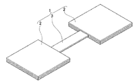
電子機器等で用いられる多層FPCは、折り曲げ可能なフレキシブル部と、多層部と称するフレキシブル基板が複数積層された部分にて構成される。
図1は多層FPCの一例を示す斜視図であり、この多層FPC1は、2つの多層部2がケーブル部3を介して接続された構造になっている。多層部2は電子部品が実装される場合が多く、リジッド板(RPC)も複合して使用される場合もあり、これはリジッド−フレックス(R−F)基板と称されている。
A multi-layer FPC used in an electronic device or the like includes a foldable flexible portion and a portion in which a plurality of flexible substrates called multi-layer portions are stacked.
FIG. 1 is a perspective view showing an example of a multilayer FPC. This multilayer FPC 1 has a structure in which two
一般に、多層部の層間接続には、貫通スルーホール(Through Hole;TH)やレーザービアホール(Laser Via Hole;LVH)などが用いられているが、これらの穴の内面には銅などのめっきを施す必要がある。高多層基板の場合、THの導電性能の信頼性を確保するためには、このめっきを厚付けしなければならない。また、所謂ビルドアッププリント配線板のようにLVHを階段状に繋げていく場合は、めっきの回数が増えるにつれて、やはりトータルのめっきが厚くならざるを得ない。このような厚いめっきがフレキシブル部にも形成されると、フレキシブル部に微細な回路を形成することが困難になるばかりでなく、フレキシブル部の最大の特長である屈曲性が失われることになる。このようにめっきが付着したフレキシブル部を無理に屈曲すれば、回路が簡単に破断してしまう。 Generally, through-holes (THrough holes; TH) and laser via holes (LVH) are used for interlayer connection in the multilayer part, and the inner surfaces of these holes are plated with copper or the like. There is a need. In the case of a high multi-layer substrate, this plating must be thickened to ensure the reliability of the TH conductive performance. Further, when LVHs are connected in a stepped manner as in a so-called build-up printed wiring board, the total plating must be thickened as the number of platings increases. If such a thick plating is also formed on the flexible portion, not only is it difficult to form a fine circuit on the flexible portion, but also the flexibility, which is the greatest feature of the flexible portion, is lost. If the flexible part to which the plating is attached is bent forcibly, the circuit is easily broken.
フレキシブル部の屈曲性を保持したまま、多層部の層間導通を取るためには、めっき工程の際に層間導通用の穴以外の部分をエッチングレジストなどで被覆しておき、めっき後に被覆を剥離する方法が既知であるが、この方法では被覆形成やその剥離のために工程数が大幅に増加し、生産性が悪くなると同時に、生産コストが増加してしまう問題がある。
この種の従来技術としては、特許文献1〜5に開示された技術が挙げられる。
In order to maintain the flexibility of the flexible part while maintaining the interlayer conduction of the multilayer part, the part other than the hole for interlayer conduction is covered with an etching resist during the plating process, and the coating is peeled off after plating. Although the method is known, this method has a problem that the number of steps is greatly increased due to the formation of the coating and the peeling thereof, the productivity is deteriorated and the production cost is increased at the same time.
Examples of this type of conventional technique include the techniques disclosed in
特許文献1には、FPCにTHを開ける前または後に所要の回路パターン部分にエッチングレジストを形成し、めっきを施し回路形成を行い、レジストを除去することにより、回路部分にめっきが付着しないため、屈曲性が良好なFPCを製造できることが開示されている。
特許文献1は、単層板(両面板)に限ったものであり、R−Fや多層FPCのような多層板に関する言及は見当たらない。また、エッチングレジストにはんだ等のめっきを用いれば、剥離後の廃液の処理コストがかかり、レジストインクのような樹脂を用いれば、露光前の仮硬化が必要となり、工程数が増加して生産性が低下してしまう。
In
特許文献2には、プリント配線板のめっきを必要としない部分にめっきを阻害するような電位をかけ、回路パターン上に選択的に無電解めっきまたは電界めっきを行う方法及び装置が開示されている。
特許文献2は、特定の回路のみに選択的にめっきするのに有効であるが、めっき装置の電極板に多数の針状電極が配置されるという極めて特殊な構造となっていることに加え、めっきをしない部分に予め形成したパッドに針状電極を接触させるためにはNC位置決め装置のような自動位置決め装置を用いなければならず、非現実的である。
特許文献3には、フレキシブル部となる片面FPCに、特定の部分が突出した外層片面FPCを銅箔層が向かい合うように積層してカバーレイで表面を覆うことで、スルーホールめっきを必要とせず層間接続を取ることができ、フレキシブル部の薄型化が可能となることが開示されている。
特許文献3では、外層片面FPCの突出部を形成する際、外層FPCを湾曲させる場合は、外層と内層の銅箔が単に物理的に接触するだけであるので、接続信頼性が得られないということが懸念される。一方、めっき等で導体を突出部に形成する場合は、導体の形成位置精度を確保することが難しい。また、特許文献3では片面FPCを向かい合わせた構造に限定されており、3層以上の多層基板への応用可能性は記載されていない。
In
特許文献4には、フレキシブル部に相当する外層を予め除去しておき、そこに離型性補助材を充填し、回路形成・めっき等の工程が終了した後に補助材を除去することによって、生産性が低下したりフレキシブル部を傷付けたりすることなくフレキシブル部が露出したR−Fプリント配線板を製造する方法が開示されている。
特許文献4では、除去した外層を補助材として再利用する実施例が示されているが、除去した外層すなわちRPCは切断端部が粗く、基材屑が品質を低下させることが懸念される。また、別の材料を充填する場合は、基板の表面平滑性を確保することが難しい。それに加えて、フレキシブル部に相当する外層を除去する前にその部分よりも少し広い範囲の銅をエッチングするため、回路形成の回数が増え、生産効率が落ちてしまう。更に高コストとなる。
In Patent Document 4, the outer layer corresponding to the flexible portion is removed in advance, filled with a releasable auxiliary material, and the auxiliary material is removed after the processes such as circuit formation and plating are completed, thereby producing A method of manufacturing an R-F printed wiring board in which a flexible portion is exposed without lowering properties or damaging the flexible portion is disclosed.
In Patent Document 4, an example in which the removed outer layer is reused as an auxiliary material is shown. However, the removed outer layer, that is, RPC has a rough cut end, and there is a concern that the base material scraps may deteriorate the quality. Moreover, when filling with another material, it is difficult to ensure the surface smoothness of the substrate. In addition, before removing the outer layer corresponding to the flexible portion, copper in a slightly wider range than that portion is etched, so that the number of circuit formation increases and the production efficiency decreases. Further, the cost is increased.
特許文献5には、FPCの屈曲部の両面に剥離可能な耐熱性フィルムをスクリーン印刷により形成し、多層部には耐熱性フィルムと同一厚さの絶縁層を形成し、銅箔層を積層後回路形成した後に、屈曲部の耐熱性フィルムを除去することで、簡単な工程で薄いR−F基板を作れることが示されている。
この提案では、耐熱性フィルムをスクリーン印刷により形成しているので、印刷後には転写や端部のだれを防ぐために熱硬化をしなければならず、工数が増加してしまう。また、銅箔層のキュアプレス時には高熱がかかるため、耐熱性フィルム中の気泡を十分に除去しておかないと、耐熱性フィルム部が膨れる虞がある。
In this proposal, since the heat-resistant film is formed by screen printing, after printing, heat curing must be performed in order to prevent the transfer and sagging of the end portion, which increases the number of steps. Further, since high heat is applied during the curing press of the copper foil layer, the heat resistant film portion may swell unless air bubbles in the heat resistant film are sufficiently removed.
本発明は前記事情に鑑みてなされ、フレキシブル部にめっきが付着することがなく、屈曲性に優れたフレキシブル部を有するFPCの製造方法の提供を目的とする。 The present invention has been made in view of the above circumstances, and an object of the present invention is to provide a method for manufacturing an FPC having a flexible portion that is excellent in flexibility without plating attached to the flexible portion.
前記目的を達成するため、本発明は、フレキシブル部以外の領域の少なくとも一部にめっき層を有するFPCの製造方法であって、FPCのフレキシブル部にマスキングテープを貼着し、次いで該FPCの表面にめっきを施し、次いで前記マスキングテープを剥離除去して、フレキシブル部以外の領域の少なくとも一部にめっき層を有すると共に、めっきが付着していないフレキシブル部を有するFPCを製造することを特徴とするFPCの製造方法を提供する。 In order to achieve the above object, the present invention is a method of manufacturing an FPC having a plating layer in at least a part of a region other than the flexible part, and a masking tape is attached to the flexible part of the FPC, and then the surface of the FPC And then removing the masking tape to produce an FPC having a plating layer in at least a part of a region other than the flexible portion and having a flexible portion to which no plating is attached. A method for manufacturing an FPC is provided.
本発明のFPCの製造方法において、前記FPCの表面にめっきを施す前に、基板に穴を開け、めっき後に基板の両面を導通するスルーホールを設けることが好ましい。 In the FPC manufacturing method of the present invention, it is preferable that a hole is formed in the substrate before plating is performed on the surface of the FPC, and a through hole is provided for conducting both surfaces of the substrate after plating.
本発明のFPCの製造方法において、前記マスキングテープを剥離除去した後、表面に回路を形成し、次いでFPCの少なくとも一方の面にカバーレイを積層してFPCを製造することが好ましい。 In the FPC manufacturing method of the present invention, it is preferable that after the masking tape is peeled and removed, a circuit is formed on the surface, and then a coverlay is laminated on at least one surface of the FPC to manufacture the FPC.
本発明のFPCの製造方法において、前記フレキシブル部以外の領域の前記カバーレイ上に外層基板を積層し、多層FPCを製造することが好ましい。 In the FPC manufacturing method of the present invention, it is preferable to manufacture a multilayer FPC by laminating an outer layer substrate on the coverlay in a region other than the flexible part.
本発明のFPCの製造方法において、前記フレキシブル部にマスキングテープを貼着する際に、該マスキングテープで覆われない部分がフレキシブル部端から2.0mm以下であることが好ましい。 In the manufacturing method of FPC of this invention, when sticking a masking tape to the said flexible part, it is preferable that the part which is not covered with this masking tape is 2.0 mm or less from an end of a flexible part.
本発明によれば、めっき前にマスキングテープをフレキシブル部に貼ることで、高価な金型を用いて精巧に打ち抜いたカバーレイを用いたり、多くの工程を経て精密にパターニングされたソルダーレジストを用いたりすることなく、フレキシブル部の屈曲特性に優れたFPCを提供することができる。 According to the present invention, a masking tape is affixed to the flexible part before plating, so that a coverlay that has been finely punched using an expensive mold is used, or a solder resist that has been precisely patterned through many steps is used. Therefore, it is possible to provide an FPC excellent in the bending characteristics of the flexible portion.
以下、図面を参照して本発明のFPCの製造方法の実施形態を説明する。
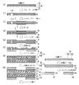
図2及び図3は、本発明の製造方法の一実施形態を示すフロー断面図であり、本実施形態では、多層FPC1として、4層リジッド−フレックス(R−F)プリント配線板を製造する場合を例示する。
Hereinafter, an embodiment of a method for producing an FPC of the present invention will be described with reference to the drawings.
2 and 3 are flow sectional views showing an embodiment of the manufacturing method of the present invention. In this embodiment, a four-layer rigid-flex (R-F) printed wiring board is manufactured as the multilayer FPC 1. Is illustrated.
本実施形態の製造方法では、まず、図2(a)に示すように、屈曲性に優れた内層FPC6を用意する。この内層FPC6としては、ポリイミドシート4の両面に導電層として銅箔5を貼り合わせてなる銅張積層板(Copper Clad Laminate;CCL)などが好適に用いられる。
In the manufacturing method of the present embodiment, first, as shown in FIG. 2A, an
次に、図2(b)に示すように、前記内層FPC6にスルーホールTHとなる穴を開ける(スルーホール穴開け工程)。本例示では、多層部2となる領域にスルーホールTHを設けている。
Next, as shown in FIG. 2B, a hole to be a through hole TH is formed in the inner layer FPC 6 (through hole drilling step). In this example, a through hole TH is provided in a region to be the
次に、図2(c)に示すように、内層FPC6のフレキシブル部3にマスキングテープ7を貼着する(マスキングテープ貼り工程)。
ここで用いるマスキングテープ7としては、次のめっき工程においてテープを貼着したフレキシブル部表面へのめっき液の浸透を防ぎ、かつ剥離時に糊残りがなく、銅箔5を傷めないテープを選択して使用することが望ましく、例えば、合成樹脂テープ基材の片面に樹脂粘着剤が積層されたマスキングテープなどが挙げられる。
Next, as shown in FIG.2 (c), the masking tape 7 is stuck on the
As the masking tape 7 used here, a tape that prevents the plating solution from penetrating into the surface of the flexible part to which the tape has been applied in the next plating step, and has no adhesive residue when peeled off, is selected so as not to damage the copper foil 5. It is desirable to use, for example, a masking tape in which a resin adhesive is laminated on one side of a synthetic resin tape substrate.
また、このマスキングテープ7は、マスキングテープで覆われない部分がフレキシブル部端から2.0mm以下であることが好ましく、特に、フレキシブル部3の全域をカバーするように貼着することが望ましい。マスキングテープで覆われない部分が2.0mmを超えると、その部分にめっき層8が形成されてフレキシブル部全体の屈曲特性が劣化し、好ましくない。
Moreover, it is preferable that this masking tape 7 is affixed so that the part which is not covered with a masking tape may be 2.0 mm or less from an end of a flexible part, and it covers especially the whole area of the
次に、図2(d)に示すように、マスキングテープ7を貼着した内層FPC6の表面にめっきを施し、内層FPC6の表面及びスルーホール7内面に銅などのめっき層8を形成する(めっき工程)。
このめっき工程は、無電解めっきや電解めっきにより行うことができる。電解銅めっきによりめっき層8を形成する場合、スルーホールTHの内面は、予め導電加工を施したり、或いはスルーホールTHの内面に無電解めっきを施して銅箔5との導電性を確保しておき、その後電解銅めっきを行ってめっき層8を形成することが望ましい。このめっきにより、スルーホールTHの内面にめっき層8が形成され、内層FPC6の両面間の電気的な導通が確保される。
Next, as shown in FIG. 2D, the surface of the
This plating step can be performed by electroless plating or electrolytic plating. When the plated
次に、図2(e)に示すように、めっきを終えた内層FPC6の表面からマスキングテープ7を剥離除去する(マスキングテープ剥がし工程)。
前述したように、剥離時に糊残りがなく、銅箔5を傷めないマスキングテープ7を使用することにより、マスキングテープ7の剥離除去が簡単に短時間で実施可能となる。
このテープ除去により、内層FPC6の表面のうち、フレキシブル部3以外の領域にめっき層8が形成され、フレキシブル部3表面にはめっき層が形成されていない内層FPC6が得られる。
Next, as shown in FIG. 2 (e), the masking tape 7 is peeled and removed from the surface of the
As described above, by using the masking tape 7 which has no adhesive residue at the time of peeling and does not damage the copper foil 5, the masking tape 7 can be peeled and removed easily in a short time.
By this tape removal, the
次に、図2(f)に示すように、内層FPC6の両面側の導電層(銅箔5及びめっき層8)を加工して所望の回路を形成する(回路形成工程)。 Next, as shown in FIG. 2 (f), a desired circuit is formed by processing the conductive layers (copper foil 5 and plating layer 8) on both sides of the inner layer FPC 6 (circuit forming step).
次に、図2(g)に示すように、回路形成を終えた内層FPC6の両面にカバーレイ11を重ね合わせ、熱プレスすることによって接着し、積層する(カバーレイ貼り工程)。
ここで用いるカバーレイ11は、内層FPC6の両面に積層後にフレキシブル部3に十分な屈曲特性が得られるものであればよく、特に制限されず、例えば、ポリイミド層9と接着剤層10を積層したものなどが用いられる。
Next, as shown in FIG. 2G, the cover lay 11 is superposed on both surfaces of the
The
なお、内層FPC6を、両面FPCとして製造する場合、前記の通り内層FPC6の両面にカバーレイ11を積層した状態でFPCを得ることができる。
本実施形態では、さらに前記内層FPC6に外層リジッド配線板(Rigid Printed Circuit;以下、RPCと記す。)を積層して図1に示す多層FPC1を製造する。
In addition, when manufacturing inner layer FPC6 as double-sided FPC, FPC can be obtained in the state which laminated | stacked the
In the present embodiment, an outer layer rigid printed circuit (hereinafter referred to as RPC) is further laminated on the
内層FPC6に積層する外層RPC14は、特に制限されないが、例えば、ガラスエポキシ板12に導電層となる銅箔13を積層した片面銅張積層板などが挙げられる。この外層RPC14は、内層FPC6に重ね合わす前に、接着シート層15を貼り付け、フレキシブル部に相当する部分を切断除去する予備工程を経て用いられる。
The
次に、図2(h)に示すように、内層FPC6の多層部2となる領域の両面に、前述した通り接着シート層15を貼り付けた外層RPC14を重ね合わせ、熱プレスすることによって積層し、多層FPC1とする(外層貼り合わせ工程)。
Next, as shown in FIG. 2 (h), the outer layer RPC14, to which the
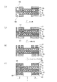
次に、図3(i)に示すように、多層FPC1の所定位置にレーザー光を照射し、内層FPC6の回路が露出するようなレーザービアホール16を穿設する(レーザー穴開け工程)。
Next, as shown in FIG. 3 (i), laser via
次に、図3(j)に示すように、多層FPC1の表面にめっきを施して、多層FPC1の表面及びレーザービアホール16内面に銅などのめっき層17を形成する(めっき工程)。
このめっき工程は、図2(d)の前記めっき工程と同様に、無電解めっきや電解めっきにより行うことができる。
このめっき層17の形成により、レーザービアホール16では、内層FPC6の回路と外層RPC14の銅箔13との電気的な導通が確保される。
なお、このめっき工程においても、事前にフレキシブル部3にマスキングテープ7を貼着してめっき形成を局部的に防止してもよい。
Next, as shown in FIG. 3J, the surface of the
This plating step can be performed by electroless plating or electrolytic plating, similarly to the plating step of FIG.
By forming the
In this plating step, the masking tape 7 may be attached to the
次に、図3(k)に示すように、外層RPC14の銅箔13を加工し、外層回路を形成する(回路形成工程)。
Next, as shown in FIG. 3 (k), the
次に、外層回路を絶縁するため、多層FPC1の多層部2表面をソルダーレジスト18によって被覆する(ソルダーレジスト形成工程)。
Next, in order to insulate the outer layer circuit, the surface of the
以上の各工程を行うことによって、図1に示すように、多層部2とフレキシブル部3とを有し、めっきが付着していないフレキシブル部3を有する多層FPC1を製造することができる。
By performing each of the above steps, as shown in FIG. 1, a
本実施形態のFPC製造方法は、めっき工程前にマスキングテープ7をフレキシブル部3に貼ることで、高価な金型を用いて精巧に打ち抜いたカバーレイを用いたり、多くの工程を経て精密にパターニングされたソルダーレジストを用いたりすることなく、フレキシブル部3の屈曲特性に優れた多層FPC1を提供することができる。
In the FPC manufacturing method of the present embodiment, the masking tape 7 is applied to the
なお、前述した実施形態は、本発明の例示に過ぎず、製造するFPCの層数や各層の厚み、構成等も、特に限定されるものではない。またR−F構造に限らず、多層FPC構造でもよい。 The above-described embodiment is merely an example of the present invention, and the number of FPC layers to be manufactured, the thickness and configuration of each layer are not particularly limited. In addition, the multilayer FPC structure is not limited to the R-F structure.
内層FPCとして両面FPCを用い、外層基板として片面RPCを用い、図2及び図3に示すように、この内層FPCの両面に外層RPCを積層した4層リジッドフレックス(R−F)プリント配線板を作製した。 As shown in FIGS. 2 and 3, a four-layer rigid flex (RF) printed wiring board is used in which a double-sided FPC is used as an inner layer FPC, a single-sided RPC is used as an outer layer substrate, and an outer layer RPC is laminated on both sides of the inner layer FPC. Produced.
<基板構成>
基板サイズ:350mm×400mm。
内層FPC:TLF−W−521 18/25/18(京セラケミカル社製、両面銅箔18μm厚、ポリイミド25μm厚)。
外層RPC:L−6504C1(ニッカン工業社製、片面銅箔18μm厚、ガラスエポキシ100μm厚)。
接着シート:TFA−880 CA35(京セラケミカル社製、接着剤層35μm)。
<Board configuration>
Substrate size: 350 mm × 400 mm.
Inner layer FPC: TLF-W-521 18/25/18 (manufactured by Kyocera Chemical Co., Ltd., double-
Outer layer RPC: L-6504C1 (manufactured by Nikkan Kogyo Co., Ltd., single-sided
Adhesive sheet: TFA-880 CA35 (manufactured by Kyocera Chemical Co., Ltd., adhesive layer 35 μm).
<基板作製手順>(図2(a)〜(h)及び図3(i)〜(l)参照)
(1)内層FPCに貫通スルーホールの穴開けをする。
(2)フレキシブル部が大凡全域覆われるように、マスキングテープを貼り付ける。フレキシブル部の端部に覆われない部分があっても問題はない。また、マスキングテープはめっき液潜りしないのであれば材質を問わない。
(3)めっきにより層間導通を取る。
(4)マスキングテープを剥がす。
(5)内層FPCの銅箔を回路形成する。
(6)カバーレイを貼り、内層FPCの表面を保護する。
(7)外層RPCに接着シートをラミネートする。
(8)接着シートをラミネート下外層RPCのフレキシブル部に相当する部分をNCルータや金型等でくり抜く。
(9)熱及び圧力により外層RPCを内層FPCに積層する。
(10)レーザー等により外層RPCとカバーレイに穴を開け、めっきにより内層との導通を取る。
(11)外層RPCの銅箔の回路形成をする。
(12)ソルダーレジスト等の表面保護膜を形成する。
<Substrate Fabrication Procedure> (See FIGS. 2 (a) to (h) and FIGS. 3 (i) to (l))
(1) Drill through holes in the inner layer FPC.
(2) A masking tape is affixed so that the flexible part is covered over the entire area. There is no problem even if there is a part that is not covered at the end of the flexible part. The masking tape may be made of any material as long as it does not dive into the plating solution.
(3) Interlayer conduction is achieved by plating.
(4) Remove the masking tape.
(5) A circuit is formed on the copper foil of the inner layer FPC.
(6) A cover lay is applied to protect the surface of the inner layer FPC.
(7) An adhesive sheet is laminated on the outer layer RPC.
(8) Cut out the part corresponding to the flexible part of the laminate lower outer layer RPC with an NC router or a mold.
(9) The outer layer RPC is laminated on the inner layer FPC by heat and pressure.
(10) A hole is made in the outer layer RPC and the coverlay with a laser or the like, and conduction with the inner layer is obtained by plating.
(11) A circuit of copper foil of the outer layer RPC is formed.
(12) A surface protective film such as a solder resist is formed.
<基板評価1>
前記手順にて作製した基板のフレキシブル部を用いて、JIS C5016 8.6の規格に準拠するような屈曲試験を行った。屈曲半径は2.5mmとした。なお、屈曲部の回路は200μmピッチ(回路幅100μm、回路間隔100μm)とした。また、実施結果の屈曲回数は、10個の試料の試験結果の平均(小数点以下四捨五入)である((1)マスキングテープ)。結果を表1に示す。
比較例として、フレキシブル部のみが完全に覆われるよう精密にパターニングしたソルダーレジストをめっき前に形成したものの結果((2)ソルダーレジスト)と、めっき工程においてフレキシブル部を被覆しなかったものの結果((3)なし)を、共に表1に示す。
<
Using the flexible part of the substrate produced in the above procedure, a bending test was performed so as to comply with the standard of JIS C5016 8.6. The bending radius was 2.5 mm. In addition, the circuit of the bent part was 200 μm pitch (circuit width 100 μm, circuit interval 100 μm). In addition, the number of bendings of the implementation results is the average (rounded off after the decimal point) of the test results of 10 samples ((1) masking tape). The results are shown in Table 1.
As a comparative example, the result of forming a solder resist precisely patterned so that only the flexible part is completely covered before plating ((2) solder resist) and the result of not coating the flexible part in the plating process (( Table 3 shows both 3) None).
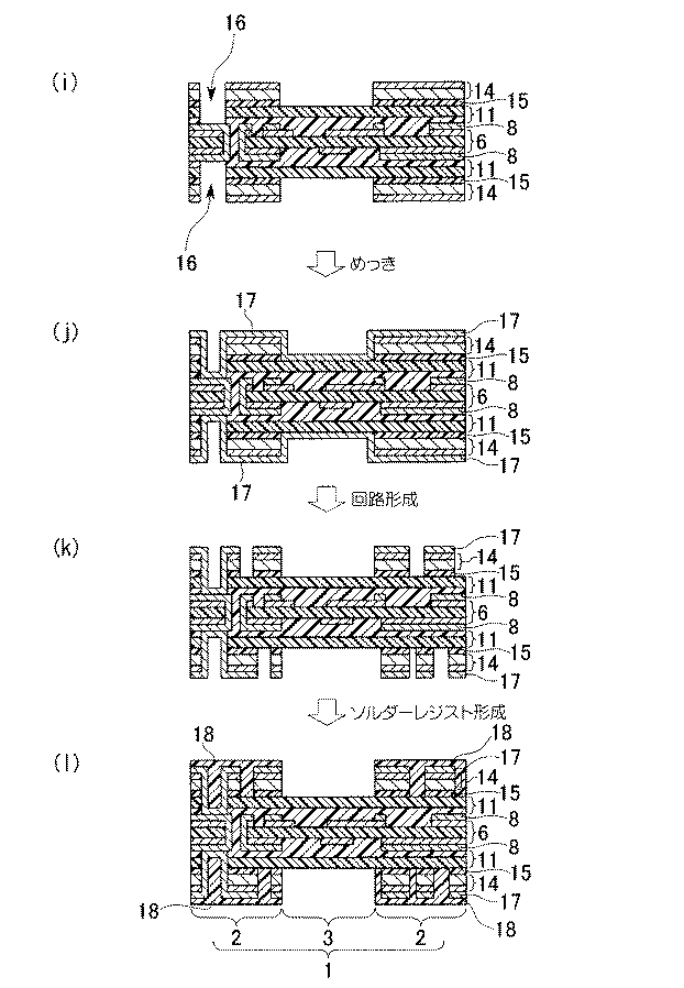
表1の結果から、マスキングテープでフレキシブル部を覆ったものは、ソルダーレジストでフレキシブル部を完全に覆ったものとほぼ同等の屈曲特性を示した。マスキングテープを貼ると、フレキシブル部の端部が覆われなくなり、そこに被っためっきによる影響が想定される。しかしながら端部のみであれば、フレキシブル部全体の屈曲特性に影響を及ぼさないことが判明した。 From the results in Table 1, the flexible part covered with the masking tape showed almost the same bending property as that completely covered the flexible part with the solder resist. When the masking tape is pasted, the end of the flexible part is not covered, and the influence of plating on the end is assumed. However, it has been found that the end portion alone does not affect the bending characteristics of the entire flexible portion.
<基板評価2>
マスキングテープの貼り合わせに必要な精度を確認するため、フレキシブル部の端部が覆われなくなるよう精密にパターニングしたソルダーレジストをめっき前に形成したものを準備し、基板評価1と同様の屈曲試験を行った。実施結果の屈曲回数は、10個の試料の試験結果の平均(小数点以下四捨五入)である。覆われない端部の幅は、(4)0.5mm、(5)1.0mm、(6)1.5mm、(7)2.0mm、(8)2.5mm、(9)3.0mmとした。結果を表2に示す。比較例として、基板評価1での(2)と(3)の試験結果を共に示す。
<
In order to confirm the accuracy required for bonding the masking tape, prepare a solder resist that is precisely patterned before plating so that the end of the flexible part is not covered. went. The number of bends in the implementation results is the average of the test results of 10 samples (rounded to the nearest decimal place). The width of the uncovered end is (4) 0.5 mm, (5) 1.0 mm, (6) 1.5 mm, (7) 2.0 mm, (8) 2.5 mm, (9) 3.0 mm It was. The results are shown in Table 2. As a comparative example, both the test results of (2) and (3) in the
表2に結果から、覆われない端部の幅が2.0mm以下のものは、いずれもほぼ(2)0mmと同等の屈曲特性を示した。(8)2.5mmになると、急激に屈曲特性が低下し、(9)3.0mmでは全く覆わなかった場合((3)被覆無し)と大差ない結果となった。めっきを被った部分が屈曲試験で実際に曲げられる部分に近いと、めっきによる応力がかかりやすくなり、屈曲特性が低下するものと考えられる。本結果より、十分な屈曲特性を得るためには2.0mm以下の精度でマスキングテープを貼る必要があることがわかった。 From the results shown in Table 2, all of the non-covered end portions having a width of 2.0 mm or less exhibited bending characteristics substantially equivalent to (2) 0 mm. (8) When the thickness is 2.5 mm, the bending characteristics are abruptly reduced, and (9) When 3.0 mm is not covered at all ((3) No coating), the result is not so different. If the part covered with plating is close to the part that is actually bent in the bending test, stress due to plating is likely to be applied, and the bending characteristics are considered to deteriorate. From this result, it was found that it was necessary to apply a masking tape with an accuracy of 2.0 mm or less in order to obtain sufficient bending characteristics.
1…多層FPC(フレキシブルプリント配線板)、2…多層部、3…ケーブル部、4…ポリイミドシート、5…銅箔、6…内層FPC、7…マスキングテープ、8…めっき層、9…ポリイミド層、10…接着剤層、11…カバーレイ、12…ガラスエポキシ板、13…銅箔、14…外層RPC、15…接着シート層、16…レーザービアホール、17…めっき層、18…ソルダーレジスト。
DESCRIPTION OF
Claims (5)
フレキシブルプリント配線板のフレキシブル部にマスキングテープを貼着し、次いで該フレキシブルプリント配線板の表面にめっきを施し、次いで前記マスキングテープを剥離除去して、フレキシブル部以外の領域の少なくとも一部にめっき層を有すると共に、めっきが付着していないフレキシブル部を有するフレキシブルプリント配線板を製造することを特徴とするフレキシブルプリント配線板の製造方法。 A method for producing a flexible printed wiring board having a plating layer in at least a part of a region other than the flexible portion,
A masking tape is attached to the flexible part of the flexible printed wiring board, then plating is performed on the surface of the flexible printed wiring board, and then the masking tape is peeled and removed to form a plating layer on at least a part of the area other than the flexible part. And manufacturing a flexible printed wiring board having a flexible part to which plating is not attached.
The flexible print according to any one of claims 1 to 4, wherein when the masking tape is attached to the flexible portion, a portion not covered with the masking tape is 2.0 mm or less from the end of the flexible portion. A method for manufacturing a wiring board.
Priority Applications (1)
| Application Number | Priority Date | Filing Date | Title |
|---|---|---|---|
| JP2005144022A JP2006324314A (en) | 2005-05-17 | 2005-05-17 | Method for manufacturing flexible printed wiring board |
Applications Claiming Priority (1)
| Application Number | Priority Date | Filing Date | Title |
|---|---|---|---|
| JP2005144022A JP2006324314A (en) | 2005-05-17 | 2005-05-17 | Method for manufacturing flexible printed wiring board |
Publications (1)
| Publication Number | Publication Date |
|---|---|
| JP2006324314A true JP2006324314A (en) | 2006-11-30 |
Family
ID=37543793
Family Applications (1)
| Application Number | Title | Priority Date | Filing Date |
|---|---|---|---|
| JP2005144022A Withdrawn JP2006324314A (en) | 2005-05-17 | 2005-05-17 | Method for manufacturing flexible printed wiring board |
Country Status (1)
| Country | Link |
|---|---|
| JP (1) | JP2006324314A (en) |
-
2005
- 2005-05-17 JP JP2005144022A patent/JP2006324314A/en not_active Withdrawn
Similar Documents
| Publication | Publication Date | Title |
|---|---|---|
| JP4499126B2 (en) | Rigid flexible printed circuit board and manufacturing method thereof | |
| JP5198105B2 (en) | Manufacturing method of multilayer flexible printed wiring board | |
| JP5313202B2 (en) | Build-up type multilayer printed wiring board and manufacturing method thereof | |
| CN101878679A (en) | Manufacturing method of multilayer printed wiring board | |
| JP2005268505A (en) | Multilayer wiring board and manufacturing method thereof | |
| US10772220B2 (en) | Dummy core restrict resin process and structure | |
| KR101229967B1 (en) | Multilayer circuit board having cable portion and method for manufacturing same | |
| JP5317491B2 (en) | Method for manufacturing printed wiring board | |
| JP2009152496A (en) | Method for manufacturing printed wiring board | |
| JP2010016061A (en) | Printed wiring board, and manufacturing method therefor | |
| JP4602783B2 (en) | Manufacturing method of rigid flex buildup wiring board | |
| JP5057653B2 (en) | Flex-rigid wiring board and manufacturing method thereof | |
| JP3155565B2 (en) | Manufacturing method of printed wiring board | |
| JP4538513B2 (en) | Manufacturing method of multilayer wiring board | |
| JP4606018B2 (en) | Method for manufacturing printed wiring board | |
| JP2005236196A (en) | Manufacturing method of multilayer wiring board | |
| JP2006324314A (en) | Method for manufacturing flexible printed wiring board | |
| JP2006156576A (en) | Manufacturing method of rigid-flex multilayer printed wiring board | |
| JP2005158923A (en) | Manufacturing method of multilayer printed wiring board | |
| JP2008034511A (en) | Manufacturing method of multilayer printed wiring board | |
| JP4347143B2 (en) | Circuit board and manufacturing method thereof | |
| JP2012169523A (en) | Manufacturing method of rigid flexible printed wiring board | |
| JP2007220735A (en) | Method for manufacturing multilayer printed wiring board having flying tail portion | |
| JP2006222114A (en) | Manufacturing method of multilayer printed wiring board | |
| JP2005109299A (en) | Multilayer wiring board and manufacturing method thereof |
Legal Events
| Date | Code | Title | Description |
|---|---|---|---|
| A300 | Withdrawal of application because of no request for examination |
Free format text: JAPANESE INTERMEDIATE CODE: A300 Effective date: 20080805 |