JP2006330082A - 湾曲量検出装置及び可撓性装置 - Google Patents
湾曲量検出装置及び可撓性装置 Download PDFInfo
- Publication number
- JP2006330082A JP2006330082A JP2005149728A JP2005149728A JP2006330082A JP 2006330082 A JP2006330082 A JP 2006330082A JP 2005149728 A JP2005149728 A JP 2005149728A JP 2005149728 A JP2005149728 A JP 2005149728A JP 2006330082 A JP2006330082 A JP 2006330082A
- Authority
- JP
- Japan
- Prior art keywords
- bending amount
- amount detection
- bending
- reference value
- detection device
- Prior art date
- Legal status (The legal status is an assumption and is not a legal conclusion. Google has not performed a legal analysis and makes no representation as to the accuracy of the status listed.)
- Granted
Links
- 239000000463 material Substances 0.000 claims abstract description 18
- 238000005452 bending Methods 0.000 claims description 89
- 238000001514 detection method Methods 0.000 claims description 65
- 239000000758 substrate Substances 0.000 claims description 36
- 230000002427 irreversible effect Effects 0.000 claims description 5
- 238000005286 illumination Methods 0.000 claims description 2
- 239000010408 film Substances 0.000 description 57
- 239000010410 layer Substances 0.000 description 15
- 239000002245 particle Substances 0.000 description 9
- 239000004973 liquid crystal related substance Substances 0.000 description 8
- 229910052782 aluminium Inorganic materials 0.000 description 6
- XAGFODPZIPBFFR-UHFFFAOYSA-N aluminium Chemical compound [Al] XAGFODPZIPBFFR-UHFFFAOYSA-N 0.000 description 6
- 238000005192 partition Methods 0.000 description 6
- 239000010409 thin film Substances 0.000 description 6
- 230000006378 damage Effects 0.000 description 5
- 238000004519 manufacturing process Methods 0.000 description 5
- 230000006866 deterioration Effects 0.000 description 4
- 239000011229 interlayer Substances 0.000 description 4
- 230000004048 modification Effects 0.000 description 4
- 238000012986 modification Methods 0.000 description 4
- 239000004642 Polyimide Substances 0.000 description 3
- 230000005489 elastic deformation Effects 0.000 description 3
- 239000007788 liquid Substances 0.000 description 3
- 229910052751 metal Inorganic materials 0.000 description 3
- 239000002184 metal Substances 0.000 description 3
- 229920001721 polyimide Polymers 0.000 description 3
- 239000000853 adhesive Substances 0.000 description 2
- 230000001070 adhesive effect Effects 0.000 description 2
- 238000000151 deposition Methods 0.000 description 2
- 230000005525 hole transport Effects 0.000 description 2
- AMGQUBHHOARCQH-UHFFFAOYSA-N indium;oxotin Chemical compound [In].[Sn]=O AMGQUBHHOARCQH-UHFFFAOYSA-N 0.000 description 2
- 238000002347 injection Methods 0.000 description 2
- 239000007924 injection Substances 0.000 description 2
- 238000000034 method Methods 0.000 description 2
- 229920005989 resin Polymers 0.000 description 2
- 239000011347 resin Substances 0.000 description 2
- 208000033748 Device issues Diseases 0.000 description 1
- 239000004988 Nematic liquid crystal Substances 0.000 description 1
- 229910052581 Si3N4 Inorganic materials 0.000 description 1
- XUIMIQQOPSSXEZ-UHFFFAOYSA-N Silicon Chemical compound [Si] XUIMIQQOPSSXEZ-UHFFFAOYSA-N 0.000 description 1
- 230000004888 barrier function Effects 0.000 description 1
- 239000006229 carbon black Substances 0.000 description 1
- 230000015556 catabolic process Effects 0.000 description 1
- 230000008859 change Effects 0.000 description 1
- 239000003795 chemical substances by application Substances 0.000 description 1
- 229920006026 co-polymeric resin Polymers 0.000 description 1
- 238000006731 degradation reaction Methods 0.000 description 1
- 230000008021 deposition Effects 0.000 description 1
- 238000004090 dissolution Methods 0.000 description 1
- 238000005401 electroluminescence Methods 0.000 description 1
- 238000001962 electrophoresis Methods 0.000 description 1
- 239000003822 epoxy resin Substances 0.000 description 1
- 238000005530 etching Methods 0.000 description 1
- 238000001746 injection moulding Methods 0.000 description 1
- 238000009413 insulation Methods 0.000 description 1
- 239000011159 matrix material Substances 0.000 description 1
- 239000003094 microcapsule Substances 0.000 description 1
- 239000003921 oil Substances 0.000 description 1
- 230000000149 penetrating effect Effects 0.000 description 1
- 229920002120 photoresistant polymer Polymers 0.000 description 1
- 239000004033 plastic Substances 0.000 description 1
- 229920003023 plastic Polymers 0.000 description 1
- 229920003229 poly(methyl methacrylate) Polymers 0.000 description 1
- 229920000647 polyepoxide Polymers 0.000 description 1
- 239000002861 polymer material Substances 0.000 description 1
- 239000004926 polymethyl methacrylate Substances 0.000 description 1
- 239000000565 sealant Substances 0.000 description 1
- 238000007789 sealing Methods 0.000 description 1
- 229910052710 silicon Inorganic materials 0.000 description 1
- 239000010703 silicon Substances 0.000 description 1
- HQVNEWCFYHHQES-UHFFFAOYSA-N silicon nitride Chemical compound N12[Si]34N5[Si]62N3[Si]51N64 HQVNEWCFYHHQES-UHFFFAOYSA-N 0.000 description 1
- 238000004528 spin coating Methods 0.000 description 1
- 239000002335 surface treatment layer Substances 0.000 description 1
Images




Landscapes
- Devices For Indicating Variable Information By Combining Individual Elements (AREA)
Abstract
【解決手段】 湾曲量検出手段(3、6、7)が、可撓性を有する基材(1)の湾曲量が、ある基準値に達したか否かを検出する。湾曲量検出手段により、基材の湾曲量が基準値に達したことが検出されると、警告発生手段(9)が、湾曲量が基準値に達したことを通知する。
【選択図】 図1
Description
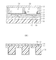
図2(A)に示すように、表面に複数の凸部2が設けられた基材1を準備する。基材1は、ポリイミドを射出成型することにより形成することができる。図2(B)に示すように、凸部2が設けられている面に、アルミニウムを真空蒸着することにより、厚さ200nmの導電膜3を形成する。図2(C)に示すように、導電膜3の表面にフォトレジストをスピンコーティングすることにより、レジスト膜Rを形成する。
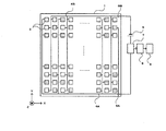
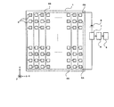
第1の実施例では、Y軸方向に長い凸部2がX軸方向に等間隔で配列していたが、第2の実施例では、複数の凸部2が行列状に、X軸方向及びY軸方向に等間隔で配置されている。凸部2の各々の上面及び側面は、第1の実施例の場合と同様に導電膜3で覆われている。X軸に平行な並びを行、Y軸に平行な並びを列としたとき、行番号と列番号との組み合わせで1つの凸部2を特定することができる。
エポキシ樹脂系接着剤48を用いて湾曲量検出装置50を透明フィルム40に貼り合わせることにより、正極41、有機発光層42、及び負極45が封止されている。湾曲量検出装置50は、上述の第1〜第3の実施例による湾曲量検出装置のいずれかと同一のものであり、凸部の付された表面が外側を向くように貼り合わせられている。
2 凸部
3 導電膜
4A、4B 配線
5A、5B 端子
6 電源
7 電流検出器
8 ドライバ回路
9 警告発生器
10 表示側基板
11 後方基板
12 隔壁
13 スイッチング素子
14 第1電極
15 層間絶縁膜
16 無機絶縁膜
17 第2電極
20 絶縁性液体
21 帯電泳動粒子
30、50、75 湾曲量検出装置
35 ペーパライクディスプレイ
35A 画像表示領域
35B 額縁領域
35C 凸部
36 枠
40 透明フィルム
41 正極
42 有機発光層
45 負極
48 接着剤
60、65 基板
61、66 透明電極
62、67 配向膜
70 間隙保持部材
71 液晶
72 シール剤
Claims (5)
- 可撓性を有する基材と、
前記基材の湾曲量が、ある基準値に達したか否かを検出する湾曲量検出手段と、
前記湾曲量検出手段により、前記基材の湾曲量が前記基準値に達したことが検出されると、湾曲量が基準値に達したことを通知する警告発生手段と
を有する湾曲量検出装置。 - 前記基材の表面に複数の凸部が設けられており、
前記湾曲量検出手段は、前記基材の凸部の各々の表面の少なくとも一部を覆う導電膜と、前記凸部のうち相互に隣り合う2つの凸部の表面を覆う導電膜に、相互に反対の極性の電圧が印加されるように、前記導電膜に電圧を印加する電圧印加手段と、相互に隣り合う2つの凸部の表面を覆う導電膜が接触して両者の間に電流が流れると、その電流を検出する電流検出手段とを含む請求項1に記載の湾曲量検出装置。 - 前記警告発生手段は、発光、発音、振動の発生、または文字の表示により、湾曲量が基準値に達したことを通知する請求項1または2に記載の湾曲量検出装置。
- 可撓性を有し、画像を表示するか、または照明光を発する機能性パネルと、
前記機能性パネルに取り付けられた請求項1〜3のいずれかに記載の湾曲量検出装置とを有し、
前記湾曲量検出装置は、前記機能性パネルの湾曲に追随して湾曲する可撓性装置。 - 前記機能性パネルに不可逆的な変形が生じる前に、前記基材の湾曲量が前記基準値に達するように、該基準値が設定されている請求項4に記載の可撓性装置。
Priority Applications (1)
| Application Number | Priority Date | Filing Date | Title |
|---|---|---|---|
| JP2005149728A JP4749764B2 (ja) | 2005-05-23 | 2005-05-23 | 湾曲検出装置及び可撓性装置 |
Applications Claiming Priority (1)
| Application Number | Priority Date | Filing Date | Title |
|---|---|---|---|
| JP2005149728A JP4749764B2 (ja) | 2005-05-23 | 2005-05-23 | 湾曲検出装置及び可撓性装置 |
Publications (2)
| Publication Number | Publication Date |
|---|---|
| JP2006330082A true JP2006330082A (ja) | 2006-12-07 |
| JP4749764B2 JP4749764B2 (ja) | 2011-08-17 |
Family
ID=37551865
Family Applications (1)
| Application Number | Title | Priority Date | Filing Date |
|---|---|---|---|
| JP2005149728A Expired - Fee Related JP4749764B2 (ja) | 2005-05-23 | 2005-05-23 | 湾曲検出装置及び可撓性装置 |
Country Status (1)
| Country | Link |
|---|---|
| JP (1) | JP4749764B2 (ja) |
Cited By (13)
| Publication number | Priority date | Publication date | Assignee | Title |
|---|---|---|---|---|
| JP2009109337A (ja) * | 2007-10-30 | 2009-05-21 | Minebea Co Ltd | 曲げセンサ |
| WO2011155117A1 (ja) * | 2010-06-09 | 2011-12-15 | シャープ株式会社 | 表示装置 |
| EP2597635A1 (en) * | 2011-11-23 | 2013-05-29 | Samsung Electronics Co., Ltd. | Display device and method for controlling the same |
| WO2014010329A1 (ja) * | 2012-07-09 | 2014-01-16 | ソニー株式会社 | 表示装置および電子機器 |
| KR20140139263A (ko) * | 2013-05-27 | 2014-12-05 | 삼성디스플레이 주식회사 | 동작 명령 안내 기능을 가지는 가요성 표시 장치 및 그 방법 |
| CN104318861A (zh) * | 2014-09-24 | 2015-01-28 | 京东方科技集团股份有限公司 | 一种柔性屏及其弯曲识别方法、柔性显示装置 |
| KR20150035232A (ko) * | 2013-09-27 | 2015-04-06 | 삼성전자주식회사 | 착용형 기기 |
| JP2015228022A (ja) * | 2014-05-06 | 2015-12-17 | 株式会社半導体エネルギー研究所 | 電子装置 |
| WO2016043215A1 (ja) * | 2014-09-19 | 2016-03-24 | 日本電気株式会社 | 表示装置の変形防止装置、変形防止方法及び変形防止プログラム |
| US9805494B2 (en) | 2012-05-11 | 2017-10-31 | Semiconductor Energy Laboratory Co., Ltd. | Electronic device, storage medium, program, and displaying method |
| US9851756B2 (en) | 2015-03-19 | 2017-12-26 | International Business Machines Corporation | Recommending bending lines on flexible displays |
| JP2018032409A (ja) * | 2012-05-31 | 2018-03-01 | 株式会社半導体エネルギー研究所 | 電子機器 |
| WO2024105715A1 (ja) * | 2022-11-14 | 2024-05-23 | 株式会社東芝 | 太陽電池シート |
Citations (3)
| Publication number | Priority date | Publication date | Assignee | Title |
|---|---|---|---|---|
| JPH0587511A (ja) * | 1991-07-24 | 1993-04-06 | Yamaha Corp | 曲げ検出装置 |
| JP2001074569A (ja) * | 1999-09-02 | 2001-03-23 | Tokin Corp | 平板型静電容量式捩り歪みセンサ |
| JP2002278515A (ja) * | 2001-03-15 | 2002-09-27 | Minolta Co Ltd | 画像表示装置 |
-
2005
- 2005-05-23 JP JP2005149728A patent/JP4749764B2/ja not_active Expired - Fee Related
Patent Citations (3)
| Publication number | Priority date | Publication date | Assignee | Title |
|---|---|---|---|---|
| JPH0587511A (ja) * | 1991-07-24 | 1993-04-06 | Yamaha Corp | 曲げ検出装置 |
| JP2001074569A (ja) * | 1999-09-02 | 2001-03-23 | Tokin Corp | 平板型静電容量式捩り歪みセンサ |
| JP2002278515A (ja) * | 2001-03-15 | 2002-09-27 | Minolta Co Ltd | 画像表示装置 |
Cited By (42)
| Publication number | Priority date | Publication date | Assignee | Title |
|---|---|---|---|---|
| JP2009109337A (ja) * | 2007-10-30 | 2009-05-21 | Minebea Co Ltd | 曲げセンサ |
| US9213195B2 (en) | 2010-06-09 | 2015-12-15 | Sharp Kabushiki Kaisha | Display device |
| WO2011155117A1 (ja) * | 2010-06-09 | 2011-12-15 | シャープ株式会社 | 表示装置 |
| EP2597635A1 (en) * | 2011-11-23 | 2013-05-29 | Samsung Electronics Co., Ltd. | Display device and method for controlling the same |
| KR20130057029A (ko) * | 2011-11-23 | 2013-05-31 | 삼성전자주식회사 | 디스플레이 장치 및 그의 제어 방법 |
| KR101879615B1 (ko) * | 2011-11-23 | 2018-07-19 | 삼성전자주식회사 | 디스플레이 장치 및 그의 제어 방법 |
| US12117872B2 (en) | 2012-05-11 | 2024-10-15 | Semiconductor Energy Laboratory Co., Ltd. | Electronic device, storage medium, program, and displaying method |
| US11216041B2 (en) | 2012-05-11 | 2022-01-04 | Semiconductor Energy Laboratory Co., Ltd. | Electronic device, storage medium, program, and displaying method |
| US10719972B2 (en) | 2012-05-11 | 2020-07-21 | Semiconductor Energy Laboratory Co., Ltd. | Electronic device, storage medium, program, and displaying method |
| US10467797B2 (en) | 2012-05-11 | 2019-11-05 | Semiconductor Energy Laboratory Co., Ltd. | Electronic device, storage medium, program, and displaying method |
| US10380783B2 (en) | 2012-05-11 | 2019-08-13 | Semiconductor Energy Laboratory Co., Ltd. | Electronic device, storage medium, program, and displaying method |
| US20190172248A1 (en) | 2012-05-11 | 2019-06-06 | Semiconductor Energy Laboratory Co., Ltd. | Electronic device, storage medium, program, and displaying method |
| US9805494B2 (en) | 2012-05-11 | 2017-10-31 | Semiconductor Energy Laboratory Co., Ltd. | Electronic device, storage medium, program, and displaying method |
| US11815956B2 (en) | 2012-05-11 | 2023-11-14 | Semiconductor Energy Laboratory Co., Ltd. | Electronic device, storage medium, program, and displaying method |
| JP2021185433A (ja) * | 2012-05-31 | 2021-12-09 | 株式会社半導体エネルギー研究所 | 電子機器 |
| JP2020060779A (ja) * | 2012-05-31 | 2020-04-16 | 株式会社半導体エネルギー研究所 | 電子機器 |
| JP2018032409A (ja) * | 2012-05-31 | 2018-03-01 | 株式会社半導体エネルギー研究所 | 電子機器 |
| US10219370B2 (en) | 2012-07-09 | 2019-02-26 | Sony Corporation | Display unit and electronic apparatus |
| US9854667B2 (en) | 2012-07-09 | 2017-12-26 | Sony Corporation | Display unit and electronic apparatus |
| US12267949B2 (en) | 2012-07-09 | 2025-04-01 | Interdigital Ce Patent Holdings, Sas | Display unit and electronic apparatus |
| WO2014010329A1 (ja) * | 2012-07-09 | 2014-01-16 | ソニー株式会社 | 表示装置および電子機器 |
| JPWO2014010329A1 (ja) * | 2012-07-09 | 2016-06-20 | ソニー株式会社 | 表示装置および電子機器 |
| US11696394B2 (en) | 2012-07-09 | 2023-07-04 | Interdigital Ce Patent Holdings, Sas | Display unit and electronic apparatus |
| US11343908B2 (en) | 2012-07-09 | 2022-05-24 | Sony Corporation | Display unit and electronic apparatus |
| US10674602B2 (en) | 2012-07-09 | 2020-06-02 | Sony Corporation | Display unit and electronic apparatus |
| KR102145568B1 (ko) * | 2013-05-27 | 2020-08-31 | 삼성디스플레이 주식회사 | 동작 명령 안내 기능을 가지는 가요성 표시 장치 및 그 방법 |
| KR20140139263A (ko) * | 2013-05-27 | 2014-12-05 | 삼성디스플레이 주식회사 | 동작 명령 안내 기능을 가지는 가요성 표시 장치 및 그 방법 |
| KR102014445B1 (ko) | 2013-09-27 | 2019-08-29 | 삼성전자주식회사 | 착용형 기기 |
| KR20150035232A (ko) * | 2013-09-27 | 2015-04-06 | 삼성전자주식회사 | 착용형 기기 |
| US11740728B2 (en) | 2014-05-06 | 2023-08-29 | Semiconductor Energy Laboratory Co., Ltd. | Electronic device |
| JP2015228022A (ja) * | 2014-05-06 | 2015-12-17 | 株式会社半導体エネルギー研究所 | 電子装置 |
| US11216106B2 (en) | 2014-05-06 | 2022-01-04 | Semiconductor Energy Laboratory Co., Ltd. | Electronic device |
| KR102495922B1 (ko) | 2014-05-06 | 2023-02-02 | 가부시키가이샤 한도오따이 에네루기 켄큐쇼 | 전자 장치 |
| US10606379B2 (en) | 2014-05-06 | 2020-03-31 | Semiconductor Energy Laboratory Co., Ltd. | Electronic device |
| KR20170005019A (ko) * | 2014-05-06 | 2017-01-11 | 가부시키가이샤 한도오따이 에네루기 켄큐쇼 | 전자 장치 |
| US12197671B2 (en) | 2014-05-06 | 2025-01-14 | Semiconductor Energy Laboratory Co., Ltd. | Electronic device |
| WO2016043215A1 (ja) * | 2014-09-19 | 2016-03-24 | 日本電気株式会社 | 表示装置の変形防止装置、変形防止方法及び変形防止プログラム |
| CN104318861A (zh) * | 2014-09-24 | 2015-01-28 | 京东方科技集团股份有限公司 | 一种柔性屏及其弯曲识别方法、柔性显示装置 |
| US9881977B2 (en) | 2014-09-24 | 2018-01-30 | Boe Technology Group Co., Ltd. | Flexible screen and bend identifying method thereof, flexible display apparatus |
| WO2016045243A1 (zh) * | 2014-09-24 | 2016-03-31 | 京东方科技集团股份有限公司 | 柔性屏及其弯曲识别方法、柔性显示装置 |
| US9851756B2 (en) | 2015-03-19 | 2017-12-26 | International Business Machines Corporation | Recommending bending lines on flexible displays |
| WO2024105715A1 (ja) * | 2022-11-14 | 2024-05-23 | 株式会社東芝 | 太陽電池シート |
Also Published As
| Publication number | Publication date |
|---|---|
| JP4749764B2 (ja) | 2011-08-17 |
Similar Documents
| Publication | Publication Date | Title |
|---|---|---|
| JP4777338B2 (ja) | 塑性変形を抑制する可撓性基材及び可撓性画像表示装置 | |
| KR101908501B1 (ko) | 터치 스크린 일체형 유기 발광 표시 장치 및 이의 제조 방법 | |
| KR102634958B1 (ko) | 보강된 부분을 갖는 배선을 포함하는 플렉서블 디스플레이디바이스 및 이의 제조 방법 | |
| JP5676554B2 (ja) | 有機発光表示装置 | |
| KR102530485B1 (ko) | 분할된 배선 패턴을 갖는 디스플레이 디바이스 | |
| CN107978625B (zh) | 柔性显示装置 | |
| CN107710313A (zh) | 柔性电子器件和柔性电子器件的制造方法 | |
| JP4749764B2 (ja) | 湾曲検出装置及び可撓性装置 | |
| JP2006048006A (ja) | 液晶表示装置及びその製造方法 | |
| KR102886683B1 (ko) | 표시 장치 | |
| JP6607762B2 (ja) | 表示装置 | |
| JP2019012098A (ja) | 表示装置 | |
| KR102611213B1 (ko) | 표시 장치 | |
| JP7473567B2 (ja) | タッチ電極構造及びその製造方法、タッチパネル及び電子機器 | |
| JP2006349788A (ja) | 電気光学装置、電気光学装置の製造方法、及び電子機器 | |
| KR102555404B1 (ko) | 플렉서블 디스플레이 및 이의 제조 방법 | |
| CN119580591B (zh) | 显示面板、拼接显示屏及电子设备 | |
| CN117241623A (zh) | 显示面板和显示装置 | |
| JP2020160393A (ja) | アクティブマトリクス基板及び液晶表示装置 | |
| CN117858436A (zh) | 均热板和包括均热板的显示装置 | |
| JP2019124761A (ja) | 表示装置 | |
| US20260007019A1 (en) | Display panel and electronic apparatus including the same | |
| WO2019102845A1 (ja) | 表示装置 | |
| KR20230161290A (ko) | 표시 장치 및 표시 장치의 제조 방법 | |
| KR20120063352A (ko) | 전기영동 표시장치 |
Legal Events
| Date | Code | Title | Description |
|---|---|---|---|
| A711 | Notification of change in applicant |
Free format text: JAPANESE INTERMEDIATE CODE: A712 Effective date: 20070201 |
|
| A621 | Written request for application examination |
Free format text: JAPANESE INTERMEDIATE CODE: A621 Effective date: 20080124 |
|
| A977 | Report on retrieval |
Free format text: JAPANESE INTERMEDIATE CODE: A971007 Effective date: 20110204 |
|
| A131 | Notification of reasons for refusal |
Free format text: JAPANESE INTERMEDIATE CODE: A131 Effective date: 20110215 |
|
| A521 | Written amendment |
Free format text: JAPANESE INTERMEDIATE CODE: A523 Effective date: 20110406 |
|
| TRDD | Decision of grant or rejection written | ||
| A01 | Written decision to grant a patent or to grant a registration (utility model) |
Free format text: JAPANESE INTERMEDIATE CODE: A01 Effective date: 20110426 |
|
| A61 | First payment of annual fees (during grant procedure) |
Free format text: JAPANESE INTERMEDIATE CODE: A61 Effective date: 20110518 |
|
| R150 | Certificate of patent or registration of utility model |
Ref document number: 4749764 Country of ref document: JP Free format text: JAPANESE INTERMEDIATE CODE: R150 Free format text: JAPANESE INTERMEDIATE CODE: R150 |
|
| FPAY | Renewal fee payment (event date is renewal date of database) |
Free format text: PAYMENT UNTIL: 20140527 Year of fee payment: 3 |
|
| R250 | Receipt of annual fees |
Free format text: JAPANESE INTERMEDIATE CODE: R250 |
|
| R250 | Receipt of annual fees |
Free format text: JAPANESE INTERMEDIATE CODE: R250 |
|
| R250 | Receipt of annual fees |
Free format text: JAPANESE INTERMEDIATE CODE: R250 |
|
| R250 | Receipt of annual fees |
Free format text: JAPANESE INTERMEDIATE CODE: R250 |
|
| R250 | Receipt of annual fees |
Free format text: JAPANESE INTERMEDIATE CODE: R250 |
|
| LAPS | Cancellation because of no payment of annual fees |