JP2006338024A - Liquid crystal display - Google Patents
Liquid crystal display Download PDFInfo
- Publication number
- JP2006338024A JP2006338024A JP2006154072A JP2006154072A JP2006338024A JP 2006338024 A JP2006338024 A JP 2006338024A JP 2006154072 A JP2006154072 A JP 2006154072A JP 2006154072 A JP2006154072 A JP 2006154072A JP 2006338024 A JP2006338024 A JP 2006338024A
- Authority
- JP
- Japan
- Prior art keywords
- electrode
- liquid crystal
- gate
- drain electrode
- crystal display
- Prior art date
- Legal status (The legal status is an assumption and is not a legal conclusion. Google has not performed a legal analysis and makes no representation as to the accuracy of the status listed.)
- Granted
Links
Images


Classifications
-
- G—PHYSICS
- G02—OPTICS
- G02F—OPTICAL DEVICES OR ARRANGEMENTS FOR THE CONTROL OF LIGHT BY MODIFICATION OF THE OPTICAL PROPERTIES OF THE MEDIA OF THE ELEMENTS INVOLVED THEREIN; NON-LINEAR OPTICS; FREQUENCY-CHANGING OF LIGHT; OPTICAL LOGIC ELEMENTS; OPTICAL ANALOGUE/DIGITAL CONVERTERS
- G02F1/00—Devices or arrangements for the control of the intensity, colour, phase, polarisation or direction of light arriving from an independent light source, e.g. switching, gating or modulating; Non-linear optics
- G02F1/01—Devices or arrangements for the control of the intensity, colour, phase, polarisation or direction of light arriving from an independent light source, e.g. switching, gating or modulating; Non-linear optics for the control of the intensity, phase, polarisation or colour
- G02F1/13—Devices or arrangements for the control of the intensity, colour, phase, polarisation or direction of light arriving from an independent light source, e.g. switching, gating or modulating; Non-linear optics for the control of the intensity, phase, polarisation or colour based on liquid crystals, e.g. single liquid crystal display cells
- G02F1/133—Constructional arrangements; Operation of liquid crystal cells; Circuit arrangements
- G02F1/136—Liquid crystal cells structurally associated with a semi-conducting layer or substrate, e.g. cells forming part of an integrated circuit
-
- G—PHYSICS
- G09—EDUCATION; CRYPTOGRAPHY; DISPLAY; ADVERTISING; SEALS
- G09G—ARRANGEMENTS OR CIRCUITS FOR CONTROL OF INDICATING DEVICES USING STATIC MEANS TO PRESENT VARIABLE INFORMATION
- G09G3/00—Control arrangements or circuits, of interest only in connection with visual indicators other than cathode-ray tubes
- G09G3/20—Control arrangements or circuits, of interest only in connection with visual indicators other than cathode-ray tubes for presentation of an assembly of a number of characters, e.g. a page, by composing the assembly by combination of individual elements arranged in a matrix no fixed position being assigned to or needed to be assigned to the individual characters or partial characters
- G09G3/34—Control arrangements or circuits, of interest only in connection with visual indicators other than cathode-ray tubes for presentation of an assembly of a number of characters, e.g. a page, by composing the assembly by combination of individual elements arranged in a matrix no fixed position being assigned to or needed to be assigned to the individual characters or partial characters by control of light from an independent source
- G09G3/36—Control arrangements or circuits, of interest only in connection with visual indicators other than cathode-ray tubes for presentation of an assembly of a number of characters, e.g. a page, by composing the assembly by combination of individual elements arranged in a matrix no fixed position being assigned to or needed to be assigned to the individual characters or partial characters by control of light from an independent source using liquid crystals
- G09G3/3611—Control of matrices with row and column drivers
- G09G3/3648—Control of matrices with row and column drivers using an active matrix
- G09G3/3659—Control of matrices with row and column drivers using an active matrix the addressing of the pixel involving the control of two or more scan electrodes or two or more data electrodes, e.g. pixel voltage dependant on signal of two data electrodes
-
- G—PHYSICS
- G02—OPTICS
- G02F—OPTICAL DEVICES OR ARRANGEMENTS FOR THE CONTROL OF LIGHT BY MODIFICATION OF THE OPTICAL PROPERTIES OF THE MEDIA OF THE ELEMENTS INVOLVED THEREIN; NON-LINEAR OPTICS; FREQUENCY-CHANGING OF LIGHT; OPTICAL LOGIC ELEMENTS; OPTICAL ANALOGUE/DIGITAL CONVERTERS
- G02F1/00—Devices or arrangements for the control of the intensity, colour, phase, polarisation or direction of light arriving from an independent light source, e.g. switching, gating or modulating; Non-linear optics
- G02F1/01—Devices or arrangements for the control of the intensity, colour, phase, polarisation or direction of light arriving from an independent light source, e.g. switching, gating or modulating; Non-linear optics for the control of the intensity, phase, polarisation or colour
- G02F1/13—Devices or arrangements for the control of the intensity, colour, phase, polarisation or direction of light arriving from an independent light source, e.g. switching, gating or modulating; Non-linear optics for the control of the intensity, phase, polarisation or colour based on liquid crystals, e.g. single liquid crystal display cells
- G02F1/133—Constructional arrangements; Operation of liquid crystal cells; Circuit arrangements
- G02F1/136—Liquid crystal cells structurally associated with a semi-conducting layer or substrate, e.g. cells forming part of an integrated circuit
- G02F1/1362—Active matrix addressed cells
- G02F1/136213—Storage capacitors associated with the pixel electrode
-
- G—PHYSICS
- G09—EDUCATION; CRYPTOGRAPHY; DISPLAY; ADVERTISING; SEALS
- G09G—ARRANGEMENTS OR CIRCUITS FOR CONTROL OF INDICATING DEVICES USING STATIC MEANS TO PRESENT VARIABLE INFORMATION
- G09G3/00—Control arrangements or circuits, of interest only in connection with visual indicators other than cathode-ray tubes
- G09G3/20—Control arrangements or circuits, of interest only in connection with visual indicators other than cathode-ray tubes for presentation of an assembly of a number of characters, e.g. a page, by composing the assembly by combination of individual elements arranged in a matrix no fixed position being assigned to or needed to be assigned to the individual characters or partial characters
- G09G3/34—Control arrangements or circuits, of interest only in connection with visual indicators other than cathode-ray tubes for presentation of an assembly of a number of characters, e.g. a page, by composing the assembly by combination of individual elements arranged in a matrix no fixed position being assigned to or needed to be assigned to the individual characters or partial characters by control of light from an independent source
- G09G3/36—Control arrangements or circuits, of interest only in connection with visual indicators other than cathode-ray tubes for presentation of an assembly of a number of characters, e.g. a page, by composing the assembly by combination of individual elements arranged in a matrix no fixed position being assigned to or needed to be assigned to the individual characters or partial characters by control of light from an independent source using liquid crystals
- G09G3/3611—Control of matrices with row and column drivers
- G09G3/3648—Control of matrices with row and column drivers using an active matrix
-
- G—PHYSICS
- G09—EDUCATION; CRYPTOGRAPHY; DISPLAY; ADVERTISING; SEALS
- G09G—ARRANGEMENTS OR CIRCUITS FOR CONTROL OF INDICATING DEVICES USING STATIC MEANS TO PRESENT VARIABLE INFORMATION
- G09G2300/00—Aspects of the constitution of display devices
- G09G2300/04—Structural and physical details of display devices
- G09G2300/0439—Pixel structures
- G09G2300/0443—Pixel structures with several sub-pixels for the same colour in a pixel, not specifically used to display gradations
-
- G—PHYSICS
- G09—EDUCATION; CRYPTOGRAPHY; DISPLAY; ADVERTISING; SEALS
- G09G—ARRANGEMENTS OR CIRCUITS FOR CONTROL OF INDICATING DEVICES USING STATIC MEANS TO PRESENT VARIABLE INFORMATION
- G09G2320/00—Control of display operating conditions
- G09G2320/02—Improving the quality of display appearance
- G09G2320/028—Improving the quality of display appearance by changing the viewing angle properties, e.g. widening the viewing angle, adapting the viewing angle to the view direction
-
- G—PHYSICS
- G09—EDUCATION; CRYPTOGRAPHY; DISPLAY; ADVERTISING; SEALS
- G09G—ARRANGEMENTS OR CIRCUITS FOR CONTROL OF INDICATING DEVICES USING STATIC MEANS TO PRESENT VARIABLE INFORMATION
- G09G3/00—Control arrangements or circuits, of interest only in connection with visual indicators other than cathode-ray tubes
- G09G3/20—Control arrangements or circuits, of interest only in connection with visual indicators other than cathode-ray tubes for presentation of an assembly of a number of characters, e.g. a page, by composing the assembly by combination of individual elements arranged in a matrix no fixed position being assigned to or needed to be assigned to the individual characters or partial characters
- G09G3/34—Control arrangements or circuits, of interest only in connection with visual indicators other than cathode-ray tubes for presentation of an assembly of a number of characters, e.g. a page, by composing the assembly by combination of individual elements arranged in a matrix no fixed position being assigned to or needed to be assigned to the individual characters or partial characters by control of light from an independent source
- G09G3/36—Control arrangements or circuits, of interest only in connection with visual indicators other than cathode-ray tubes for presentation of an assembly of a number of characters, e.g. a page, by composing the assembly by combination of individual elements arranged in a matrix no fixed position being assigned to or needed to be assigned to the individual characters or partial characters by control of light from an independent source using liquid crystals
- G09G3/3611—Control of matrices with row and column drivers
- G09G3/3648—Control of matrices with row and column drivers using an active matrix
- G09G3/3655—Details of drivers for counter electrodes, e.g. common electrodes for pixel capacitors or supplementary storage capacitors
Landscapes
- Physics & Mathematics (AREA)
- Engineering & Computer Science (AREA)
- Chemical & Material Sciences (AREA)
- Crystallography & Structural Chemistry (AREA)
- General Physics & Mathematics (AREA)
- Nonlinear Science (AREA)
- Computer Hardware Design (AREA)
- Theoretical Computer Science (AREA)
- Microelectronics & Electronic Packaging (AREA)
- Mathematical Physics (AREA)
- Optics & Photonics (AREA)
- Power Engineering (AREA)
- Liquid Crystal (AREA)
- Devices For Indicating Variable Information By Combining Individual Elements (AREA)
- Thin Film Transistor (AREA)
- Liquid Crystal Display Device Control (AREA)
- Control Of Indicators Other Than Cathode Ray Tubes (AREA)
Abstract
【課題】視認性を改善すると共に二つの副画素の透過率を所望の水準に調整し、各副画素電極に大きさが異なる電圧を印加することによるキックバック電圧の不均衡をなくして、フリッカーが発生しない構造を提供し、同時に開口率の減少を最小限に抑制する液晶装置を提供する。
【解決手段】行列状に配列され第1及び第2副画素電極を有する複数の画素電極、複数の維持電極、第1及び第2画素電極にそれぞれ接続され維持電極と重畳する複数の第1及び第2ドレイン電極を備える。第1副画素電極の面積は、第2副画素電極の面積より大きく、第1ドレイン電極と維持電極が重畳する面積が第2ドレイン電極と維持電極が重畳する面積より大きいが、第1副画素電極に第2副画素電極より低いデータ電圧が印加されるときに対応して、第1ドレイン電極の下部に維持電極の延長部をさらに設けて、第1ストレージキャパシタの容量をより大きくする。
【選択図】図4Flicker that improves visibility and adjusts the transmittance of two subpixels to a desired level, eliminates an imbalance of kickback voltages by applying voltages of different sizes to each subpixel electrode, and flicker Provided is a liquid crystal device that provides a structure that does not cause the occurrence of an aperture and simultaneously suppresses a decrease in aperture ratio to a minimum.
A plurality of pixel electrodes arranged in a matrix and having first and second subpixel electrodes, a plurality of sustain electrodes, a plurality of first and second electrodes connected to the first and second pixel electrodes and overlapping the sustain electrodes, respectively. A second drain electrode is provided. The area of the first subpixel electrode is larger than the area of the second subpixel electrode, and the area where the first drain electrode and the sustain electrode overlap is larger than the area where the second drain electrode and the sustain electrode overlap. Corresponding to when a data voltage lower than that of the second subpixel electrode is applied to the electrode, an extension portion of the sustain electrode is further provided below the first drain electrode to further increase the capacitance of the first storage capacitor.
[Selection] Figure 4
Description
本発明は液晶表示装置に関する。 The present invention relates to a liquid crystal display device.
液晶表示装置は、現在最も広く用いられている平板表示装置の一つであって、画素電極と共通電極など電界生成電極が形成されている二枚の表示板と、その間に挟持された液晶層とからなり、電界生成電極に電圧を印加して液晶層に電界を生成し、これによって液晶層の液晶分子の配向を決定し入射光の偏光を制御することで映像を表示する。 The liquid crystal display device is one of the most widely used flat display devices at present, and includes two display plates on which electric field generating electrodes such as a pixel electrode and a common electrode are formed, and a liquid crystal layer sandwiched therebetween A voltage is applied to the electric field generating electrode to generate an electric field in the liquid crystal layer, thereby determining the orientation of the liquid crystal molecules in the liquid crystal layer and controlling the polarization of incident light, thereby displaying an image.
特に、電界が印加されない状態で液晶分子の長軸を上下表示板に対して垂直をなすように配列した垂直配向モード液晶表示装置は、コントラスト比が大きく、広い基準視野角の実現が容易なため脚光を浴びている。ここで、基準視野角とは、コントラスト比が1:10の視野角または階調間の輝度反転限界角度を意味する。
垂直配向モード液晶表示装置で広視野角を実現するための手段としては、電界生成電極に切開部を形成する方法と、電界生成電極上に突起を形成する方法などがある。切開部と突起で液晶分子が傾く方向を決定できるので、これによって液晶分子の傾斜方向を複数方向に分散させて基準視野角を広くすることができる。
In particular, a vertical alignment mode liquid crystal display device in which the long axes of liquid crystal molecules are aligned perpendicular to the upper and lower display plates in the absence of an electric field has a large contrast ratio and can easily realize a wide reference viewing angle. In the spotlight. Here, the reference viewing angle means a viewing angle having a contrast ratio of 1:10 or a luminance inversion limit angle between gradations.
As means for realizing a wide viewing angle in the vertical alignment mode liquid crystal display device, there are a method of forming an incision in the electric field generating electrode, a method of forming a protrusion on the electric field generating electrode, and the like. Since the direction in which the liquid crystal molecules are tilted can be determined by the incision portion and the protrusion, the tilt direction of the liquid crystal molecules can be dispersed in a plurality of directions, thereby widening the reference viewing angle.
しかし、垂直配向モードの液晶表示装置は、前面視認性に比較して側面視認性が劣る。例えば、切開部を有するPVA(patterned vertically aligned)モードの液晶表示装置の場合、側面に向かうほど画像が明るくなり、ひどい場合は、高階調間の輝度差が無くなって画像がぼやけてしまう問題が生じる。
側面視認性を改善するために、一つの画素を二つの副画素に分割し、二つの副画素を容量性結合した後、一方の副画素には直接電圧を印加し、もう一方の副画素には容量性結合による電圧降下を生じさせ、二つの副画素の電圧を異にして透過率を異なるようにする方法が提示された。
However, the liquid crystal display device in the vertical alignment mode is inferior in side visibility compared with front visibility. For example, in the case of a liquid crystal display device in a PVA (patterned vertically aligned) mode having an incision, the image becomes brighter toward the side, and if it is severe, there is a problem that there is no luminance difference between high gradations and the image is blurred. .
In order to improve the side visibility, one pixel is divided into two subpixels, the two subpixels are capacitively coupled, and then a voltage is directly applied to one subpixel and the other subpixel is applied. Proposed a method of causing a voltage drop due to capacitive coupling, and making the transmittances different by making the voltages of the two sub-pixels different.
しかしながら、この方法は、二つの副画素の透過率を所望の水準に正確に調整することが難しく、特に色相によって光透過率が異なるため、各色相に対する電圧配合を異ならせる必要があるが、これを実行することができない。また、容量性結合のための導電体の追加などによる開口率の低下が現れ、容量性結合による電圧降下によって透過率が減少する。 However, in this method, it is difficult to accurately adjust the transmittance of the two sub-pixels to a desired level. In particular, since the light transmittance varies depending on the hue, it is necessary to change the voltage composition for each hue. Can not run. In addition, the aperture ratio decreases due to the addition of a conductor for capacitive coupling, and the transmittance decreases due to a voltage drop due to capacitive coupling.
そこで、本発明は、上記のような従来の問題点を解決するためになされたものであって、その目的は、視認性を改善すると共に二つの副画素の透過率を所望の水準に調整し、各副画素電極に大きさが異なる電圧を印加することによるキックバック電圧の不均衡をなくして、フリッカーが発生しない構造を提供し、同時に開口率の減少を最小限に抑制する液晶表示装置を提供することにある。 Therefore, the present invention has been made to solve the conventional problems as described above, and its purpose is to improve visibility and adjust the transmittance of two subpixels to a desired level. A liquid crystal display device that provides a structure in which flicker is not generated by eliminating imbalance in kickback voltage by applying voltages of different sizes to each sub-pixel electrode, and at the same time suppressing a decrease in aperture ratio to a minimum It is to provide.
上述した目的を達成するために本発明では、第1ドレイン電極の延長部と重なるように維持電極に接続されたゲート導電体を敷設して第1ストレージキャパシタの保持容量をより大きくしたり、第2ストレージキャパシタの保持容量をより小さくしたりして、低階調電圧が印加される第1画素電極のキックバック電圧と、高階調電圧が印加される第2画素電極のキックバック電圧の均衡をとり、同時に開口率に悪影響を及ぼさずにストレージキャパシタを形成することができる。 In order to achieve the above-described object, in the present invention, a gate conductor connected to the sustain electrode is laid so as to overlap with the extension of the first drain electrode to increase the storage capacity of the first storage capacitor, (2) Reducing the storage capacity of the storage capacitor to balance the kickback voltage of the first pixel electrode to which the low gradation voltage is applied and the kickback voltage of the second pixel electrode to which the high gradation voltage is applied. At the same time, the storage capacitor can be formed without adversely affecting the aperture ratio.
上記目的を達成するためになされた本発明の一特徴による液晶表示装置は、基板上に形成される第1ゲート電極と、前記基板上に形成され、前記第1ゲート電極と分離されている維持電極と、前記第1ゲート電極及び前記維持電極上に形成されるゲート絶縁膜と、前記ゲート絶縁膜上に形成される第1半導体と、前記第1半導体上に形成される第1ソース電極と、前記第1半導体層上に形成され、前記第1ソース電極と分離され、前記第1ゲート電極と重畳する端部、前記維持電極と重畳して該端部と離れている拡張部、及び該端部と該拡張部を接続する接続部を有する第1ドレイン電極と、前記第1ソース電極及び第1ドレイン電極上に形成され、前記第1ドレイン電極の拡張部を露出させるコンタクトホール(接触孔)を有する保護膜と、前記コンタクトホールを介して前記第1ドレイン電極に接続される第1電場生成電極とを備え、前記維持電極は、前記第1ドレイン電極の拡張部と重畳する本体部と、前記第1ドレイン電極の接続部と重畳する延長部とを有する。 In order to achieve the above object, a liquid crystal display device according to one aspect of the present invention is provided with a first gate electrode formed on a substrate, and maintained on the substrate and separated from the first gate electrode. An electrode, a gate insulating film formed on the first gate electrode and the sustain electrode, a first semiconductor formed on the gate insulating film, and a first source electrode formed on the first semiconductor An end portion formed on the first semiconductor layer, separated from the first source electrode and overlapping the first gate electrode, an extension portion overlapping the sustain electrode and separated from the end portion; and A first drain electrode having a connection portion connecting the end portion and the extension portion; and a contact hole (contact hole) formed on the first source electrode and the first drain electrode and exposing the extension portion of the first drain electrode. And a protective film having A first electric field generating electrode connected to the first drain electrode through the contact hole, and the sustain electrode includes a body portion overlapping with an extended portion of the first drain electrode, and the first drain electrode It has an extension part which overlaps with a connection part.
前記第1ドレイン電極の拡張部の境界は、前記維持電極の本体部の境界線内に位置し、前記維持電極の延長部は、前記維持電極の一部から分岐することが望ましく、前記維持電極の延長部の幅は、前記第1ドレイン電極の接続部の幅より広くてもよい。
前記保護膜上に形成され、前記第1電場生成電極に印加される電圧と異なる大きさの電圧が印加される第2電場生成電極をさらに備えることが望ましく、前記第1電場生成電極と第2電場生成電極とは容量性結合されることが望ましい。
Preferably, the boundary of the extended portion of the first drain electrode is located within the boundary line of the main body of the sustain electrode, and the extended portion of the sustain electrode branches off from a part of the sustain electrode. The width of the extended portion may be wider than the width of the connecting portion of the first drain electrode.
It is preferable to further include a second electric field generating electrode formed on the protective film and applied with a voltage having a magnitude different from the voltage applied to the first electric field generating electrode. It is desirable that the electric field generating electrode be capacitively coupled.
また、前記基板上に形成される第2ゲート電極と、前記ゲート絶縁膜上に形成される第2半導体と、前記第2半導体上に形成される第2ソース電極と、前記第2半導体上に形成され、前記第2ソース電極と分離され、前記第2電場生成電極に接続される第2ドレイン電極とをさらに備え、前記第1電場生成電極と前記第2電場生成電極とは、一つの映像情報から得られた互いに異なる大きさのデータ電圧の印加を受けることができる。
前記第2ドレイン電極は、前記維持電極の本体部と重畳することができ、前記第2ドレイン電極と前記維持電極の本体部との重畳面積は、前記第1ドレイン電極と前記維持電極の本体部との重畳面積より小さくてもよく、前記維持電極の本体部において、前記第2ドレイン電極と重畳する部分の幅は、前記第1ドレイン電極と重畳する部分の幅より狭くてもよい。前記維持電極の本体部において、前記第2ドレイン電極と重畳する部分の長さは、前記第1ドレイン電極と重畳する部分の長さより短くてもよい。
前記第1電場生成電極には、所定の電圧に対し前記第2電場生成電極より低い電圧が印加されてもよく、前記第1電場生成電極の面積は、前記第2電場生成電極の面積より大きくてもよい。
A second gate electrode formed on the substrate; a second semiconductor formed on the gate insulating film; a second source electrode formed on the second semiconductor; and the second semiconductor. A second drain electrode formed and separated from the second source electrode and connected to the second electric field generating electrode, wherein the first electric field generating electrode and the second electric field generating electrode are one image. Data voltages of different magnitudes obtained from information can be applied.
The second drain electrode may overlap with the main body of the sustain electrode, and an overlapping area between the second drain electrode and the main body of the sustain electrode may be the first drain electrode and the main body of the sustain electrode. The width of the portion overlapping the second drain electrode in the main body portion of the sustain electrode may be smaller than the width of the portion overlapping the first drain electrode. In the main body of the sustain electrode, the length of the portion overlapping the second drain electrode may be shorter than the length of the portion overlapping the first drain electrode.
The first electric field generating electrode may be applied with a voltage lower than the second electric field generating electrode with respect to a predetermined voltage, and the area of the first electric field generating electrode is larger than the area of the second electric field generating electrode. May be.
また、前記第1ゲート電極に接続される第1ゲート線と、前記第2ゲート電極に接続される第2ゲート線と、前記第1及び第2ソース電極に接続されるデータ線とをさらに備えることが望ましい。
また、前記第1及び第2ゲート電極に接続されるゲート線と、前記第1ソース電極に接続される第1データ線と、前記第2ソース電極に接続される第2データ線とをさらに備えることが望ましい。
A first gate line connected to the first gate electrode; a second gate line connected to the second gate electrode; and a data line connected to the first and second source electrodes. It is desirable.
A gate line connected to the first and second gate electrodes; a first data line connected to the first source electrode; and a second data line connected to the second source electrode. It is desirable.
上記目的を達成するためになされた本発明の他の特徴による液晶表示装置は、行列状に配列され第1及び第2副画素を有する複数の画素と、前記第1及び第2副画素に接続される複数の第1信号線と、前記第1信号線と交差し第1副画素に接続される第2信号線と、前記第1信号線と交差し第2副画素に接続される第3信号線とを備え、前記第1副画素は、前記第1及び第2信号線に接続される第1スイッチング素子、及び該第1スイッチング素子に接続される第1液晶キャパシタと第1ストレージキャパシタとを有し、前記第2副画素は、前記第1及び第3信号線に接続される第2スイッチング素子、及び該第2スイッチング素子に接続される第2液晶キャパシタと第2ストレージキャパシタとを有し、前記第1及び第2液晶キャパシタに印加される電圧は一つの映像情報から得られ、前記第1副画素には所定の電圧に対し前記第2副画素より低い電圧が印加され、前記第1及び第2副画素に同一電圧が印加されるときに、前記第1及び第2副画素のキックバック電圧の大きさを実質的に同一にする第1及び第2ストレージキャパシタの静電容量を各々第1及び第2容量とする場合、前記第1ストレージキャパシタの静電容量が前記第1容量より大きくても、前記第2ストレージキャパシタの容量が前記第2容量より小さくてもよい。 In order to achieve the above object, a liquid crystal display device according to another aspect of the present invention includes a plurality of pixels arranged in a matrix and having first and second subpixels, and connected to the first and second subpixels. A plurality of first signal lines, a second signal line that crosses the first signal line and is connected to the first subpixel, and a third signal that crosses the first signal line and is connected to the second subpixel. A first switching element connected to the first and second signal lines; a first liquid crystal capacitor connected to the first switching element; a first storage capacitor; The second subpixel includes a second switching element connected to the first and third signal lines, and a second liquid crystal capacitor and a second storage capacitor connected to the second switching element. And the first and second liquid crystal capacitors The applied voltage is obtained from one piece of video information, a voltage lower than the second subpixel is applied to the first subpixel with respect to a predetermined voltage, and the same voltage is applied to the first and second subpixels. When the capacitances of the first and second storage capacitors that make the magnitudes of the kickback voltages of the first and second subpixels substantially the same are the first and second capacitors, respectively, The capacitance of the first storage capacitor may be larger than the first capacitance, or the capacitance of the second storage capacitor may be smaller than the second capacitance.
前記第1スイッチング素子は第1ゲート電極と第1ドレイン電極とを有し、前記第2スイッチング素子は第2ゲート電極と第2ドレイン電極とを有し、前記第1及び第2ストレージキャパシタは、前記第1及び第2ゲート電極と分離され、本体部とこれから分岐した延長部を有する維持電極を共通に有し、前記第1ストレージキャパシタは前記維持電極と前記第1ドレイン電極との重畳からなり、前記第2ストレージキャパシタは前記維持電極と前記第2ドレイン電極との重畳からなり、前記第1液晶キャパシタは前記第1スイッチング素子に接続される第1副画素電極を有し、前記第2液晶キャパシタは前記第2スイッチング素子に接続される第2副画素電極を有することが望ましい。
前記第1ドレイン電極は、前記第1ゲート電極と重畳する端部、前記維持電極と重畳し該端部と離れている拡張部、及び該端部と該拡張部を接続する接続部を有し、前記維持電極の本体部は、前記第1ドレイン電極の拡張部及び前記第2ドレイン電極と重畳し、前記維持電極の延長部は、前記第1ドレイン電極の接続部と重畳することができる。
前記第1ドレイン電極の拡張部の境界は、前記維持電極の本体部の境界線内に位置し、前記維持電極の延長部の幅は、前記第1ドレイン電極の接続部の幅より広くてもよく、前記維持電極の本体部において前記第2ドレイン電極と重畳する部分の幅は、前記第1ドレイン電極の拡張部と重畳する部分の幅より狭くてもよい。
前記第1副画素電極の面積は前記第2副画素電極の面積より大きく、前記維持電極と前記第1ドレイン電極とが重畳する面積は、前記維持電極と前記第2ドレイン電極とが重畳する面積より大きくてもよい。
The first switching element has a first gate electrode and a first drain electrode, the second switching element has a second gate electrode and a second drain electrode, and the first and second storage capacitors are: The first and second gate electrodes are separated from each other and have a sustain electrode having a main body portion and an extension portion branched therefrom, and the first storage capacitor is formed by overlapping the sustain electrode and the first drain electrode. The second storage capacitor is formed by superimposing the sustain electrode and the second drain electrode, and the first liquid crystal capacitor has a first subpixel electrode connected to the first switching element, and the second liquid crystal The capacitor preferably has a second subpixel electrode connected to the second switching element.
The first drain electrode has an end portion that overlaps the first gate electrode, an extension portion that overlaps the sustain electrode and is separated from the end portion, and a connection portion that connects the end portion and the extension portion. The body portion of the sustain electrode may overlap the extension portion of the first drain electrode and the second drain electrode, and the extension portion of the sustain electrode may overlap the connection portion of the first drain electrode.
The boundary of the extended portion of the first drain electrode is located within the boundary line of the main body portion of the sustain electrode, and the width of the extended portion of the sustain electrode may be wider than the width of the connection portion of the first drain electrode. The width of the portion overlapping the second drain electrode in the main body of the sustain electrode may be narrower than the width of the portion overlapping the extended portion of the first drain electrode.
The area of the first subpixel electrode is larger than the area of the second subpixel electrode, and the area where the sustain electrode and the first drain electrode overlap is the area where the sustain electrode and the second drain electrode overlap. It may be larger.
このような本発明の液晶表示装置によれば、一つの画素電極を二つの副画素電極に分割し、二つの副画素電極に別途の互いに異なるデータ電圧を印加することによって、側面視認性を向上させることができる。また、低い電圧が印加される第1副画素電極の第1ドレイン電極の接続部の下に維持電極の延長部をさらに設けたり、第2ドレイン電極が維持電極と重畳する面積などを調節したりすることによって、互いに異なる電圧を印加することによる液晶キャパシタの容量変化に対応してストレージキャパシタの容量を調節し、二つの副画素のキックバック電圧の均衡をとることができ、この結果、フリッカーなどの画質劣化を防止することができる。また、ドレイン電極の接続部の下に維持電極の延長部をさらに設けることによって、保持容量を充分に確保しながら維持電極の面積を減少させることができるので、開口率を一層増加させることができる。 According to the liquid crystal display device of the present invention, side visibility is improved by dividing one pixel electrode into two subpixel electrodes and applying different data voltages to the two subpixel electrodes. Can be made. Further, an extension portion of the sustain electrode is further provided below the connection portion of the first drain electrode of the first subpixel electrode to which a low voltage is applied, or an area where the second drain electrode overlaps with the sustain electrode is adjusted. Thus, the capacitance of the storage capacitor can be adjusted in response to the capacitance change of the liquid crystal capacitor by applying different voltages, and the kickback voltage of the two subpixels can be balanced. Image quality degradation can be prevented. Further, by further providing an extension portion of the sustain electrode below the connection portion of the drain electrode, the area of the sustain electrode can be reduced while ensuring a sufficient storage capacity, so that the aperture ratio can be further increased. .
次に、本発明の液晶表示装置を実施するための最良の形態の具体例を、図面を参照しながら説明する。しかし、本発明は、多様な形態で実現することができ、ここで説明する実施形態に限定されない。
図面は、各種層及び領域を明確に表現するために、厚さを拡大して示している。明細書全体を通じて類似した部分については同一な参照符号を付けている。層、膜、領域、板などの部分が、他の部分の“上に”あるとする時、これは他の部分の“すぐ上に”ある場合に限らず、その中間に更に他の部分がある場合も含む。逆に、ある部分が他の部分の“すぐ上に”あるとする時、これは中間に他の部分がない場合を意味する。
Next, a specific example of the best mode for carrying out the liquid crystal display device of the present invention will be described with reference to the drawings. However, the present invention can be realized in various forms and is not limited to the embodiments described herein.
In the drawings, the thickness is enlarged to clearly show various layers and regions. Similar parts are denoted by the same reference numerals throughout the specification. When a layer, film, region, plate, or other part is “on top” of another part, this is not limited to “immediately above” another part, and another part is in the middle. Including some cases. Conversely, when a part is “just above” another part, this means that there is no other part in the middle.
以下、本発明の一実施形態による液晶表示装置について図1乃至図5を参照して詳細に説明する。
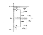
図1乃至図3は、本発明の一実施形態による液晶表示装置のブロック図(その1〜その3)であり、図4は、本発明の一実施形態による液晶表示装置の一つの画素に対する等価回路図、図5は、本発明の一実施形態による液晶表示装置の一つの副画素に対する等価回路図である。
Hereinafter, a liquid crystal display according to an exemplary embodiment of the present invention will be described in detail with reference to FIGS.
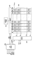
1 to 3 are block diagrams (
図1乃至図3に示すように、本発明の一実施形態による液晶表示装置は、液晶表示板組立体300と、これに接続された一対または一つのゲート駆動部400a、400b、400、及びデータ駆動部500、データ駆動部500に接続された階調電圧生成部800、並びにこれらを制御する信号制御部600を備える。
As shown in FIGS. 1 to 3, a liquid crystal display according to an embodiment of the present invention includes a liquid
液晶表示板組立体300は、等価回路的に複数の表示信号線(G1a−Gnb、D1−Dm)と、これに接続されてほぼ行列状に配列された複数の画素PXを有する。一方、図5に示すように、液晶表示板組立体300は、互いに対向する下部及び上部表示板100、200と、両者間に挟持された液晶層3を有する。
表示信号線(G1a−Gnb、D1−Dm)は下部表示板100に備えられ、ゲート信号(走査信号とも言う)を伝達する複数対のゲート線(G1a−Gnb)とデータ信号を伝達するデータ線(D1−Dm)を有する。ゲート線(G1a−Gnb)はほぼ行方向に延びて互いにほぼ平行であり、データ線(D1−Dm)はほぼ列方向に延びて互いにほぼ平行である。
The liquid
Display signal lines (G 1a -G nb , D 1 -D m ) are provided on the
図4には、表示信号線と一つの画素PXの等価回路が示されているが、図面符号GLa、GLbで示した一対のゲート線と、図面符号DLで示したデータ線以外にも、表示信号線は、ゲート線GLa、GLbとほぼ平行に延びた維持電極線SLをさらに有する。
各画素PXは一対の副画素PXa、PXbを有し、各副画素PXa、PXbはゲート線GLa、GLb及びデータ線DLに接続されているスイッチング素子Qa、Qbと、これに接続された液晶キャパシタCLCa、CLCb、並びにスイッチング素子Qa、Qb及び維持電極線SLに接続されているストレージキャパシタCSTa、CSTbを有する。
FIG. 4 shows an equivalent circuit of the display signal line and one pixel PX. In addition to the pair of gate lines indicated by the drawing symbols GLa and GLb and the data line indicated by the drawing symbol DL, a display is also provided. The signal line further includes a storage electrode line SL extending substantially parallel to the gate lines GLa and GLb.
Each pixel PX has a pair of subpixels PXa and PXb. Each subpixel PXa and PXb has switching elements Qa and Qb connected to the gate lines GLa and GLb and the data line DL, and a liquid crystal capacitor connected thereto. C LC a, C LC b, and storage capacitors C ST a, C ST b connected to the switching elements Qa, Qb and the storage electrode line SL are included.
図5に示すように、各副画素PXa、PXbのスイッチング素子Qは、下部表示板100に備えられている薄膜トランジスタなどからなり、ゲート線GLに接続されている制御端子、データ線DLに接続されている入力端子、そして液晶キャパシタCLC及びストレージキャパシタCSTに接続されている出力端子を有する三端子素子である。
As shown in FIG. 5, the switching element Q of each of the sub-pixels PXa and PXb includes a thin film transistor provided in the
液晶キャパシタCLCは、下部表示板100の副画素電極PEと上部表示板200の共通電極CEを二つの端子とし、二つの電極PE、CE間の液晶層3は誘電体として機能する。副画素電極PEはスイッチング素子Qに接続され、共通電極CEは上部表示板200の全面に形成され、共通電圧Vcomの印加を受ける。図5と異なり、共通電極CEが下部表示板100に備えられる場合もあり、その場合には、二つの電極PE、CEのうちの少なくとも一つが線状または棒状に形成できる。
In the liquid crystal capacitor CLC , the sub-pixel electrode PE of the
液晶キャパシタCLCの補助的な役割を果たすストレージキャパシタCSTは、下部表示板100に備えられた維持電極線SLと副画素電極PEが絶縁体を介在して重畳してなり、維持電極線SLには共通電圧Vcomなど定められた電圧が印加される。しかし、ストレージキャパシタCSTは、副画素電極PEが絶縁体を媒介としてすぐ上の前段ゲート線と重畳してなることもできる。
An auxiliary role storage capacitor C ST of the liquid crystal capacitor C LC is electrode line SL and the sub-pixel electrode PE maintained which is provided on the
一方、色表示を実現するために、各画素PXが基本色のうちの一つを固有に表示したり(空間分割)、各画素PXが時間によって交互に基本色を表示(時間分割)したりするようにして、これら三原色の空間的、時間的な作用で所望の色相が認識されるようにする。基本色の例としては赤色、緑色及び青色の三原色がある。
図5は、空間分割の一例であり、各画素PXが上部表示板200の領域に基本色のうちの一つを示すカラーフィルタCFを備えているものを示す。図5と異なり、カラーフィルタCFは下部表示板100の副画素電極PEの上または下に設けることもできる。
On the other hand, in order to realize color display, each pixel PX uniquely displays one of the basic colors (space division), or each pixel PX alternately displays the basic color according to time (time division). Thus, the desired hue is recognized by the spatial and temporal effects of these three primary colors. Examples of basic colors include the three primary colors red, green and blue.
FIG. 5 shows an example of space division, in which each pixel PX includes a color filter CF indicating one of the basic colors in the area of the
図1乃至図3に示すように、ゲート駆動部400a、400b、400は、ゲート線(G1a−Gnb)に接続されて外部からのゲートオン電圧Vonとゲートオフ電圧Voffの組み合わせからなるゲート信号をゲート線(G1a−Gnb)に印加する。図1は、一対のゲート駆動部400a、400bがそれぞれ液晶表示板組立体300の左右に位置し、奇数番目及び偶数番目のゲート線(G1a−Gnb)にそれぞれ接続され、図2及び図3に示した一つのゲート駆動部400は、液晶表示板組立体300の一方に位置し、全てのゲート線(G1a−Gnb)に接続されており、図3に示すように、ゲート駆動部400内に二つの駆動回路401、402が内蔵されてそれぞれ奇数番目及び偶数番目のゲート線(G1a−Gnb)に接続される。
As shown in FIGS. 1 to 3, the
階調電圧生成部800は、画素PXの透過率に関連する二つの階調電圧群(または基準階調電圧群)を生成する。二つの階調電圧群は一つの画素PXを構成する二つの副画素PXa、PXbにそれぞれ独立して提供されるもので、各階調電圧群は、共通電圧Vcomに対してプラスの値を有するものと、マイナスの値を有するものを含む。しかし、二つの(基準)階調電圧群の代わりに一つの(基準)階調電圧群だけ生成することもできる。
The
データ駆動部500は、液晶表示板組立体300のデータ線(D1−Dm)に接続されて階調電圧生成部800からの二つの階調電圧群のうちの一つを選択し、選択された階調電圧群に属する一つの階調電圧をデータ電圧として画素PXに印加する。しかし、階調電圧生成部800が全階調に対する電圧を全て提供するのではなく、基準階調電圧のみを提供する場合、データ駆動部500は、基準階調電圧を分圧して全階調に対する階調電圧を生成し、この中からデータ電圧を選択する。
The
ゲート駆動部400、400a、400bまたはデータ駆動部500は、一つ以上の駆動集積回路チップ形態に液晶表示板組立体300上に直接装着されたり、フレキシブル印刷回路膜(図示せず)上に装着されてTCP(tape carrier package)形態にされたりして液晶表示板組立体300に付着することもできる。これに対し、ゲート駆動部400、400a、400bまたはデータ駆動部500を液晶表示板組立体300に集積することもできる。
信号制御部600は、ゲート駆動部400及びデータ駆動部500などの動作を制御する。
The
The
次に、このような液晶表示板組立体の構造について図6乃至図10を参照して詳細に説明する。
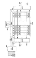
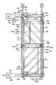
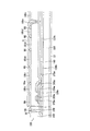
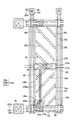
図6は、本発明の一実施形態による液晶表示装置用薄膜トランジスタ表示板の配置図であり、図7は、本発明の一実施形態による共通電極表示板の配置図であり、図8は、図6及び図7の二つの表示板を備える液晶表示板組立体の配置図であり、図9及び図10は各々図8の液晶表示板組立体のVIIA−VIIA線及びVIIB−VIIB′−VIIB″線に沿った断面図である。
図6乃至図10に示すように、本発明の一実施形態による液晶表示板組立体は、薄膜トランジスタ表示板100、共通電極表示板200、これら二つの表示板100、200の間に挟持された液晶層3を備える。
Next, the structure of such a liquid crystal panel assembly will be described in detail with reference to FIGS.
FIG. 6 is a layout view of a thin film transistor array panel for a liquid crystal display according to an embodiment of the present invention, FIG. 7 is a layout view of a common electrode display panel according to an embodiment of the present invention, and FIG. FIG. 9 is a layout view of a liquid crystal panel assembly having two display panels of FIG. 6 and FIG. 7, and FIG. 9 and FIG. 10 are lines VIIA-VIIA and VIIB-VIIB′-VIIB ″ of the liquid crystal panel assembly of FIG. It is sectional drawing along a line.
6 to 10, the liquid crystal panel assembly according to an embodiment of the present invention includes a thin
まず、図6、図8、図9及び図10を参照して薄膜トランジスタ表示板100について詳細に説明する。
透明なガラスまたはプラスチックなどからなる絶縁基板110上に、複数対の第1及び第2ゲート線121a、121bと複数の維持電極線131を有する複数のゲート導電体が形成されている。
第1及び第2ゲート線121a、121bはゲート信号を伝達し、主に横方向に延びており、それぞれ上側及び下側に位置する。
First, the thin film
A plurality of gate conductors having a plurality of pairs of first and
The first and
第1ゲート線121aは、下方に突出した複数の第1ゲート電極124aと他の層または外部駆動回路との接続のために、広い面積を有しそれぞれ左側に配置された端部129aを有する。
第2ゲート線121bは、上方に突出した複数の第2ゲート電極124bと他の層または外部駆動回路との接続のために、広い面積を有し左側に配置された端部129bを有する。
The
The
しかし、第1及び第2ゲート線の端部129a、129bは両方とも右側に配置されてもよく、互いに異なる側に配置されてもよい。ゲート信号を生成するゲート駆動回路(図示せず)は、基板110上に付着されるフレキシブル印刷回路膜(図示せず)上に装着されたり、基板110上に直接装着されたりして、基板110に集積できる。ゲート駆動回路が基板110上に集積され場合、ゲート線121a、121bが延びてこれと直接接続させることができる。
However, both the
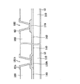
維持電極線131は所定の電圧の印加を受け、主に横方向に延びている。各維持電極線131は、第1及び第2ゲート線121a、121bの間に位置し、第2ゲート線121bよりも第1ゲート線121aにより近く、隣接した二つの第2ゲート線121bとほぼ同一距離をおいている。各維持電極線131は、上下に拡張された維持電極137と、維持電極137から上方に長く延びた棒状の延長部139を有する。維持電極137はほぼ長方形で、維持電極線131に対称であり、延長部139は第1ゲート電極124aの右側近傍まで延びている。しかし、維持電極137と延長部139を始めとする維持電極線131の形状及び配置はいろいろな形態に変形可能である。
The
ゲート導電体121a、121b、131は、アルミニウム(Al)やアルミニウム合金などアルミニウム系金属、銀(Ag)や銀合金など銀系金属、銅(Cu)や銅合金など銅系金属、モリブデン(Mo)やモリブデン合金などモリブデン系金属、クロム(Cr)、タンタル(Ta)及びチタニウム(Ti)などからなることができる。しかし、これらは物理的性質が異なる二つの導電膜(図示せず)を有する多重膜構造を有することもできる。このうちの一つの導電膜は、信号遅延や電圧降下を減らすことができるように比抵抗が低い金属、例えば、アルミニウム系金属、銀系金属、銅系金属などからなる。これに対し、もう一つの導電膜は、他の物質、特にITO(indium tin oxide)及びIZO(indium zinc oxide)との物理的、化学的、電気的接触特性に優れた物質、例えばモリブデン系金属、クロム、タンタル、チタニウムなどからなる。
The
このような組み合わせの良い例としては、クロム下部膜とアルミニウム(合金)上部膜、及びアルミニウム(合金)下部膜とモリブデン(合金)上部膜がある。しかし、ゲート導電体121a、121b、131は、これ以外にも様々な金属または導電体からなることができる。
ゲート導電体121a、121b、131の側面は基板110面に対し傾斜しており、その傾斜角は約30°乃至約80゜であることが好ましい。
Good examples of such a combination include a chromium lower film and an aluminum (alloy) upper film, and an aluminum (alloy) lower film and a molybdenum (alloy) upper film. However, the
The side surfaces of the
ゲート導電体121a、121b、131上には、SiNxまたはSiOxなどからなるゲート絶縁膜140が形成されている。
ゲート絶縁膜140上には、水素化非晶質シリコン(非晶質シリコンはa−Siと略称する。)または多結晶シリコンなどからなる複数の島状の半導体154a、154b、156a、157aが形成されている。半導体154a、154bは、それぞれ第1及び第2ゲート電極124a、124b上に位置する。半導体156a、157aは、第1及び第2ゲート線121a、121b、維持電極線131、維持電極137及び延長部139の境界を覆う。
A
A plurality of island-shaped
半導体154a、154b、156a上には、複数の島状のオーミック接触部材(ohmic contact)163a、163b、165a、165b、166aが形成されており、半導体157a上にも島状オーミック接触部材(図示せず)が形成されている。オーミック接触部材163a、163b、165a、165b、166aは、リンなどのn型不純物が高濃度にドーピングされているn+水素化非晶質シリコンなどの物質からなるか、シリサイド(silicide)からなることができる。オーミック接触部材163a、165aとオーミック接触部材163b、165bとは、それぞれ対をなして半導体154a、154b上に配置される。
半導体154a、154b、156a、157aとオーミック接触部材163a、163b、165a、165b、166aの側面も基板110面に対し傾斜しており、その傾斜角は30°乃至80°程度である。
オーミック接触部材163a、163b、165a、165b、166a及びゲート絶縁膜140上には、複数のデータ線171と複数対の第1及び第2ドレイン電極175a、175bを有するデータ導電体が形成されている。
A plurality of island-shaped
The side surfaces of the
A data conductor having a plurality of
データ線171は、データ信号を伝達し、主に縦方向に延びて第1、第2ゲート線121a、121b及び維持電極線131と交差する。各データ線171は、第1及び第2ゲート電極124a、124bに向かって延びた複数の第1及び第2ソース電極173a、173bと他の層または外部駆動回路との接続のために広い面積の端部179を有する。データ信号を生成するデータ駆動回路(図示せず)は、基板110上に付着されるフレキシブル印刷回路膜(図示せず)上に装着されたり、基板110上に直接装着されたりして、基板110に集積できる。データ駆動回路が基板110上に集積される場合、データ線171が延びてこれと直接接続できる。
The
第1及び第2ドレイン電極175a、175bは互いに分離されており、データ線171とも分離されている。
第1ドレイン電極175aは、第1ゲート電極124aを中心に第1ソース電極173aと対向する棒状の端部176a、棒状の端部176aの反対側端にある広い長方形の拡張部177a、そして拡張部177aと端部176aを接続する線状の接続部176aaを有する。拡張部177aは維持電極137と重畳し、棒状の端部176aは第1ゲート電極124aと重畳し、C字状に折曲した第1ソース電極173aで一部覆われている。第1ドレイン電極175aの接続部176aaはほとんど延長部139上に位置し、延長部139と平行に延びており、延長部139の縦境界線内に位置する。
The first and
The
同様に、第2ドレイン電極175bは、第2ゲート電極124bを中心に第2ソース電極173bと対向する棒状の端部176b、棒状の端部176bの反対側端にある広い長方形の拡張部177b、そして拡張部177bと端部176bを接続する線状の接続部176bbを有する。拡張部177bは維持電極137と重畳し、棒状の端部176bは第2ゲート電極124bと重畳し、C字状に折曲した第2ソース電極173bで一部覆われている。第2ドレイン電極175bの拡張部177bの面積は、第1ドレイン電極175aの拡張部177aの面積より小さい。
Similarly, the
このように、第1ドレイン電極175aの接続部176aa下に延長部139を設けて保持容量を増加させることができるので、維持電極137の面積を小さくして開口率を高めることができる。
第1、第2ゲート電極124a、124b、第1、第2ソース電極173a、173b、及び第1、第2ドレイン電極175a、175bは、第1、第2半導体154a、154bと共に第1、第2薄膜トランジスタ(TFT)Qa、Qbを構成し、第1、第2薄膜トランジスタQa、Qbのチャンネルは、第1、第2ソース電極173a、173bと第1、第2ドレイン電極175a、175bとの間の第1、第2半導体154a、154bに形成される。
As described above, since the
The first and
データ導電体171、175a、175bは、モリブデン、クロム、タンタル及びチタニウムなどの耐火性金属、またはこれらの合金からなることが望ましく、耐火性金属膜(図示せず)と低抵抗導電膜(図示せず)を有する多重膜構造を有することができる。多重膜構造の例としては、クロムまたはモリブデン(合金)下部膜とアルミニウム(合金)上部膜の二重膜、モリブデン(合金)下部膜とアルミニウム(合金)中間膜とモリブデン(合金)上部膜の三重膜がある。しかし、データ導電体171、175a、175bは、これ以外にも様々な金属または導電体からなることができる。
データ導電体171、175a、175bもその側面が基板110面に対し30°乃至80°程度の角度で傾斜していることが好ましい。
The
The side surfaces of the
オーミック接触部材163a、163b、165a、165b、166aは、その下の第1及び第2半導体154a、154bとその上のデータ導電体171、175a、175bとの間にのみ存在し、これらの間の接触抵抗を低くする。第1、第2ゲート線121a、121b及び維持電極線131上に位置した第1及び第2半導体156a、157aは、表面のプロファイルを滑らかにしてデータ線171及び第1、第2ドレイン電極175a、175bの断線を防止する。島状の第1及び第2半導体154a、154bには、第1及び第2ソース電極173a、173bと第1及び第2ドレイン電極175a、175bとの間を始めとするデータ導電体171、175a、175bで覆われず露出した部分がある。
The
データ導電体171、175a、175b及び露出した第1、第2半導体154a、154b上には、保護膜180が形成されている。保護膜180は、無機絶縁物または有機絶縁物などからなり、表面が平坦化されることができる。無機絶縁物の例としては、窒化ケイ素と酸化ケイ素がある。有機絶縁物は感光性を有することができ、その誘電定数は約4.0以下であることが好ましい。しかし、保護膜180は、有機膜の優れた絶縁特性を保ちながら露出した第1及び第2半導体154a、154b部分に悪影響を及ぼさないように、下部無機膜と上部有機膜の二重膜構造を有することができる。
A
保護膜180にはデータ線171の端部179及び第1及び第2ドレイン電極175a、175bの拡張部177a、177bをそれぞれ露出させる複数のコンタクトホール(接触孔)182、185a、185bが形成されており、保護膜180とゲート絶縁膜140には第1及び第2ゲート線121a、121bの端部129a、129bを露出させる複数のコンタクトホール181a、181bが形成されている。
The
保護膜180上には、第1及び第2副画素電極191a、191bを有する複数の画素電極191、遮蔽電極88、及び複数の接触補助部材81a、81b、82が形成されている。これらはITOまたはIZOなどの透明な導電物質やアルミニウム、銀、クロム、またはその合金などの反射性金属からなることができる。
各画素電極191は、4つの角が面取りされた(chamfered)ほぼ四角形状であり、面取りされた斜辺は第1及び第2ゲート線121a、121bに対して約45度の角度をなしている。
A plurality of
Each
各画素電極191を構成する一対の第1及び第2副画素電極191a、191bは、ギャップ(gap)92を間に挟んで互いに噛み合っている。第2副画素電極191bは、ほぼ直角に回転した等辺台形で、下辺が台形に凹んで、ほとんどが第1副画素電極191aで覆われている。第1副画素電極191aは、左側辺で互いに連結されている上部、下部及び中央の台形部からなる。
The pair of first and
第1副画素電極191aは、上部台形部の上辺及び下部台形部の下辺から右側辺に向かって延びた切開部93a、93b、93c、94a、94b、94cを有する。切開部93a、94aと切開部93b、94bとの間をゲート線121aが通過する。第1副画素電極191aの中央台形部は、第2副画素電極191bの凹んだ下辺に嵌合されている。また、第1副画素電極191aは、横部及びこれに接続された一対の斜線部を有する中央切開部91を有する。横部は、第1副画素電極191aの横中心線に沿って短く延びており、一対の斜線部は横部から第1副画素電極191aの左側辺に向かって延び、維持電極線131に対して約45度の角度をなしている。第1副画素電極191aと第2副画素電極191bとの間のギャップ92は、ゲート線121a、121bと約45度をなしている二対の上部及び下部斜線部と三つの縦部を有する。以下、説明の便宜上、ギャップ92も切開部と称する。
The
切開部91−94cは、維持電極線131に対してほとんど反転対称をなし、これらは第1及び第2ゲート線121a、121bに対して約45度の角度をなして互いに垂直に延びている。画素電極191は、これら切開部91−94cによって複数の領域に分割される。
これにより、画素電極191を横方向に二等分する維持電極線131を中心にした上半部と下半部は、切開部91−94cによりそれぞれ6個の領域に分けられる。
ここで、領域の数または切開部の数は、画素電極191の大きさ、画素電極191の横辺と縦辺の長さ比、液晶層3の種類や特性など、設計要素によって変化する。
The incisions 91-94c are almost inversion symmetric with respect to the
Accordingly, the upper half and the lower half around the
Here, the number of regions or the number of cutouts varies depending on design factors such as the size of the
第1及び第2副画素電極191a、191bは、それぞれコンタクトホール185a、185bを介して第1及び第2ドレイン電極175a、175bに接続されており、第1及び第2ドレイン電極175a、175bからデータ電圧の印加を受ける。一対の副画素電極191a、191bには、一つの入力映像信号に対し予め設定されている互いに異なるデータ電圧が印加され、その大きさは第1及び第2副画素電極191a、191bの大きさ及び形状によって設定される。また、第1及び第2副画素電極191a、191bの面積は互いに異なることができる。例えば、第2副画素電極191bは、第1副画素電極191aに比較して高い電圧の印加を受け、第1副画素電極191aより面積が小さい。
The first and
データ電圧が印加された第1及び第2副画素電極191a、191bと共通電圧の印加を受ける共通電極270は、第1及び第2液晶キャパシタCLCa、CLCbを構成し、第1、第2薄膜トランジスタQa、Qbが非導通状態になった後も印加された電圧を維持する。各液晶キャパシタCLCa、CLCbは、液晶層3部分を誘電体として有する。
第1及び第2副画素電極191a、191b及びこれに電気的に接続された第1及び第2ドレイン電極175a、175bの拡張部177a、177bは、維持電極137及び延長部139を始めとする維持電極線131と重畳して第1及び第2液晶キャパシタCLCa、CLCbの電圧維持能力を強化する第1及び第2ストレージキャパシタCSTa、CSTbを構成する。
The first and
遮蔽電極88は、データ線171に沿って延びた縦部と第2ゲート線121bに沿って延びた横部を有しており、縦部はデータ線171を完全に覆い、横部は第2ゲート線121bの境界線の内側に位置している。
遮蔽電極88は、共通電圧Vcomの印加を受け、データ線171と画素電極191の間及びデータ線171と共通電極270との間に形成される電界を遮断して、画素電極191の電圧歪曲及びデータ線171が伝達するデータ電圧の信号遅延が減少する。しかし、必要に応じて遮蔽電極88は省略してもよい。
The
The
接触補助部材81a、81b、82は、それぞれコンタクトホール181a、181b、182を介して第1、第2ゲート線121a、121bの端部129a、129b及びデータ線171の端部179に接続される。接触補助部材81a、81b、82は、第1、第2ゲート線121a、121bの端部129a、129b及びデータ線171の端部179と外部装置との接着性を補完し、これらを保護する。
The
次に、図7乃至図10を参照して、共通電極表示板200について説明する。
透明なガラスまたはプラスチックなどからなる絶縁基板210上に、遮光部材220が形成されている。遮光部材220は、ブラックマトリックスとも言い、光漏洩を防ぐ。遮光部材220は、画素電極191と対向しており、画素電極191とほぼ同一形状の複数の開口部225を有している。これに対し、遮光部材220は、データ線171に対応する部分と、第1、第2薄膜トランジスタQa、Qbに対応する部分からなることもできる。遮光部材220は、画素電極191と薄膜トランジスタQa、Qb近傍の光漏洩を遮断するために様々な形状を有することができる。
Next, the
A
また、基板210上には、複数のカラーフィルタ230が形成されており、遮光部材220で覆われた領域内にほとんど位置している。カラーフィルタ230は、画素電極191に沿って縦方向に長く延びることができる。カラーフィルタ230は赤色、緑色及び青色などの基本色のうちの一つを表示することができる。
A plurality of
カラーフィルタ230及び遮光部材220上には、オーバーコート膜(overcoat)250が形成されている。オーバーコート膜250は、(有機)絶縁物からなることができ、カラーフィルタ230が露出するのを防止し、平坦面を提供する。
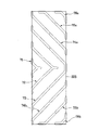
オーバーコート膜250上には共通電極270が形成されている。共通電極270はITO、IZOなどの透明な導電体などからなり、複数の切開部群71、72、73、74a、74b、75a、75b、76a、76bを有する。
An
A
一つの切開部群71−76bは、一つの画素電極191と対向し、中央切開部71、72、73、上部切開部74a、75a、76a及び下部切開部74b、75b、76bを有する。切開部71−76bのそれぞれは、画素電極191の隣接切開部91−94cの間、または切開部91、94a、94b、94cと画素電極191の面取りされた斜辺、または左側辺の間に配置されている。また、各切開部71−76bは、画素電極の切開部91−94cと平行に延びた少なくとも一つの斜線部を有する。
One incision group 71-76b is opposed to one
上部及び下部切開部74a−76bのそれぞれは、斜線部と横部及び縦部を有する。斜線部はほぼ画素電極191の右側辺から上側または下側辺に画素電極191上部または下部切開部93a−94cとほぼ平行に延びる。横部及び縦部は、斜線部の各端から画素電極191の辺に沿って辺と重畳しながら延び、斜線部と鈍角をなしている。
Each of the upper and
中央切開部71、72は、中央横部、一対の斜線部及び一対の縦断縦部を有する。中央横部は、ほぼ画素電極191の横中心線に沿って短く延び、一対の斜線部は、中央横部の端から画素電極191の左側辺に向かってそれぞれ下部及び上部切開部74a−76bとほぼ平行に延びている。縦断縦部は、斜線部の各端から画素電極191の左側辺に沿って重畳しながら延び、斜線部と鈍角をなしている。
The
切開部73−76bの斜線部には、三角形状のノッチ(notch)が形成されている。ノッチは四角形、台形または半円形に形成されたり、突出した形状や凹んだ形状に形成されたりすることもできる。このノッチは、切開部71−76bに対応する領域の境界に位置する液晶分子3の配列方向を決定する。
切開部71−76bの数及び方向も設計要素によって変わり、遮光部材220が切開部71〜76bと重畳して切開部71−76b近傍の光漏洩を遮断することができる。
A triangular notch is formed in the hatched portion of the incision 73-76b. The notches can be formed in a square shape, a trapezoidal shape, or a semicircular shape, or can be formed in a protruding shape or a recessed shape. This notch determines the alignment direction of the
The number and direction of the incisions 71-76b also vary depending on the design elements, and the
下部及び上部表示板100、200の内側面には配向膜11、21が塗布されており、これは垂直配向膜とすることができる。
下部及び上部表示板100、200の外側面には偏光子を有する偏光板12、22が備えられており、二つの偏光子を有する偏光板12、22の相互の偏光軸は直交し、このうちの一つの偏光軸は、第1及び第2ゲート線121a、121bに対して平行であることが望ましい。反射型液晶表示装置では、二つの偏光板12、22のうちの一つは省略してもよい。
Polarizers 12 and 22 having polarizers are provided on the outer surfaces of the lower and
本実施形態による液晶表示装置は、液晶層3の遅延値を補償するための位相遅延膜(図示せず)をさらに備えることができる。位相遅延膜は、複屈折性を有し、液晶層3の位相遅延を逆に補償する。
液晶層3は負の誘電率異方性を有し、液晶層3の液晶分子は電場がない状態でその長軸が二つの表示板100、200の表面に対して垂直をなすように配向されている。このため、入射光は二つの偏光板12、22の直交する偏光子を通過できず遮断される。
The liquid crystal display device according to the present embodiment may further include a phase retardation film (not shown) for compensating for the delay value of the
The
共通電極270に共通電圧を印加し、画素電極191にデータ電圧を印加して、第1または第2液晶キャパシタCLCa、CLCbの両端に電位差が生じれば、下部及び上部表示板100、200の面にほぼ垂直である電場が液晶層3に生成される(以下、画素電極191及び共通電極270を電場生成電極という。)。すると、液晶層3の液晶分子は電場に応答してその長軸が電場の方向に対して垂直をなすように傾斜し、液晶分子が傾いた程度によって液晶層3に入射された光の偏光の変化程度が変わる。このような偏光の変化は、二つの偏光板12、22の偏光子により透過率の変化として現れ、これによって液晶表示装置は映像を表示する。
If a common voltage is applied to the
液晶分子の傾斜角度は電場の強さによって変化し、第1副画素電極191aには低い電圧が印加され、第2副画素電極には高い電圧が印加されれば、第1液晶キャパシタCLCaの電圧Vaが第2液晶キャパシタCLCbの電圧Vbより大きいので、第1副画素Xaと第2副画素Xbで液晶分子の傾斜角度が異なり、これによって二つの副画素PXa、PXbの輝度が異なる。この結果、第1液晶キャパシタCLCaの電圧Vaと、第2液晶キャパシタCLCbの電圧Vbを適切に調整すれば、側面から見る映像が正面から見る映像に最大限に近付けることができ、これによって側面視認性を向上させることができる。
The inclination angle of the liquid crystal molecules is changed depending on the intensity of the electric field, the
液晶分子の傾斜方向は、電場生成電極191、270の切開部71−76b、91−94cと画素電極191の斜辺が電場を歪曲して形成する水平成分によって決定され、この電場の水平成分は、切開部71−76b、91−94cの辺と画素電極191の辺に垂直である。
The tilt direction of the liquid crystal molecules is determined by a horizontal component formed by distorting the electric field by the incisions 71-76b and 91-94c of the electric
図8に示すように、一つの切開部群71−76b、91−94cは、画素電極191をそれぞれ二つの傾いた主辺(major edge)を有する複数の副領域(sub−area)に分け、各副領域の液晶分子の傾斜方向は、電場の水平成分により決定される方向に決定され、傾斜方向はほぼ4つの方向である。このように液晶分子の傾斜方向を複数にすれば、液晶表示装置の基準視野角が大きくなる。
As shown in FIG. 8, each incision group 71-76b, 91-94c divides the
液晶分子の傾斜方向を決定するための切開部71−76b、91−94cの形状及び配置は変形することができ、少なくとも一つの切開部71−76b、91−94cは、突起(図示せず)や陥没部(図示せず)で代替してもよい。突起は有機物または無機物からなることができ、電場生成電極191、270の上または下に配置できる。
The shape and arrangement of the incisions 71-76b and 91-94c for determining the tilt direction of the liquid crystal molecules can be modified, and at least one of the incisions 71-76b and 91-94c is a protrusion (not shown). Alternatively, a depression (not shown) may be substituted. The protrusion may be made of an organic material or an inorganic material, and may be disposed on or below the electric
次に、このような液晶表示装置の表示動作について図1乃至図4を参照して詳細に説明する。
信号制御部600は、外部のグラフィック制御部(図示せず)から入力映像信号R、G、B及びその表示を制御する入力制御信号、例えば、垂直同期信号Vsyncと水平同期信号Hsync、メインクロックMCLK、データイネーブル信号DEなどの提供を受ける。信号制御部600は、入力映像信号R、G、Bと入力制御信号に基づいて映像信号R、G、Bを液晶表示板組立体300の動作条件に合せて適切に処理し、ゲート制御信号CONT1及びデータ制御信号CONT2などを生成した後、ゲート制御信号CONT1をゲート駆動部400に送出し、データ制御信号CONT2と処理した映像信号DATはデータ駆動部500に送出する。
Next, the display operation of such a liquid crystal display device will be described in detail with reference to FIGS.
The
ゲート制御信号CONT1は、ゲートオン電圧Vonの走査開始を指示する走査開始信号STVと、ゲートオン電圧Vonの出力を制御する少なくとも一つのクロック信号などを有する。
データ制御信号CONT2は、一つの画素行のデータ伝送を知らせる水平同期開始信号STH(図示せず)と、データ線(D1−Dm)に当該データ電圧の印加を指示するロード信号LOAD、及びデータクロック信号HCLK(共に図示せず)を有する。また、データ制御信号CONT2は、共通電圧Vcomに対するデータ電圧の極性(以下、共通電圧に対するデータ電圧の極性を略してデータ電圧の極性という。)を反転させる反転信号RVS(図示せず)を有することができる。
The gate control signal CONT1 includes a scan start signal STV for instructing start of scanning of the gate-on voltage Von, at least one clock signal for controlling the output of the gate-on voltage Von, and the like.
The data control signal CONT2 includes a horizontal synchronization start signal STH (not shown) for notifying data transmission of one pixel row, a load signal LOAD for instructing application of the data voltage to the data lines (D 1 -D m ), and It has a data clock signal HCLK (both not shown). The data control signal CONT2 has an inversion signal RVS (not shown) for inverting the polarity of the data voltage with respect to the common voltage Vcom (hereinafter, the polarity of the data voltage with respect to the common voltage is abbreviated as the polarity of the data voltage). Can do.
信号制御部600からのデータ制御信号CONT2に従って、データ駆動部500は、一群の副画素PXa、PXbに対する映像信号DATを受信し、階調電圧生成部800からの二つの階調電圧群のうちの一群を選択し、選択された階調電圧郡の中から各映像データDATに対応する階調電圧を選択することによって、映像信号DATを当該データ電圧に変換した後、これを当該データ線(D1−Dm)に印加する。
In accordance with the data control signal CONT2 from the
これと異なり、データ駆動部500ではなく別個に備えられた外部の選択回路(図示せず)で二つの階調電圧群のうちのいずれか一つを選択してデータ駆動部500に伝達することや、階調電圧生成部800により値が変化する基準電圧を提供し、データ駆動部500はこれを分圧して自ら階調電圧を形成することもできる。
Unlike this, instead of the
ゲート駆動部400、400a、400bは、信号制御部600からのゲート制御信号CONT1に従ってゲートオン電圧Vonをゲート線(G1a−Gnb)に印加して、該ゲート線(G1a−Gnb)に接続されたスイッチング素子Qa、Qbを導通させ、これによってデータ線(D1−Dm)に印加されたデータ電圧が導通したスイッチング素子Qa、Qbを介して当該副画素PXa、PXbに印加される。
The
副画素PXa、PXbに印加されたデータ電圧と共通電圧Vcomの差は液晶キャパシタCLCa、CLCbの充電電圧、つまり、画素電圧として現れる。液晶分子は画素電圧の大きさによってその配列が異なり、このため液晶層3を通過する光の偏光が変化する。このような偏光の変化は、下部及び上部表示板100、200に付着された偏光板12の偏光子によって光透過率の変化として現れる。
A difference between the data voltage applied to the sub-pixels PXa and PXb and the common voltage Vcom appears as a charging voltage of the liquid crystal capacitors C LC a and C LC b, that is, a pixel voltage. The arrangement of the liquid crystal molecules varies depending on the magnitude of the pixel voltage. For this reason, the polarization of light passing through the
前述した二つの階調電圧群は互いに異なるガンマ曲線を示し、これらが一つの画素PXの二つの副画素PXa、PXbに印加されるので、一つの画素PXのガンマ曲線はこれらを合成した曲線となる。二つの階調電圧群を決定する際には、合成ガンマ曲線が正面の基準ガンマ曲線に近接するようにする。例えば、正面の合成ガンマ曲線は、最も好適に定められた正面の基準ガンマ曲線と一致するようにし、側面の合成ガンマ曲線は、正面の基準ガンマ曲線に最も近接するようにする。この結果、側面視認性が向上する。 The two gradation voltage groups described above show different gamma curves, and these are applied to the two sub-pixels PXa and PXb of one pixel PX. Therefore, the gamma curve of one pixel PX is a combined curve. Become. When determining the two gradation voltage groups, the combined gamma curve is set close to the front reference gamma curve. For example, the front composite gamma curve should match the most suitably defined front reference gamma curve, and the side composite gamma curve should be closest to the front reference gamma curve. As a result, side visibility is improved.
なお、既に説明したように、高い電圧の印加を受ける第2副画素電極191bの面積を第1副画素電極191aの面積より小さくすることで、側面ガンマ曲線の歪みを小さくすることができる。特に、第1及び第2副画素電極191a、191bの面積比率がほぼ2:1であるとき、側面ガンマ曲線が正面ガンマ曲線により近接して、側面視認性が一層良くなる。
As already described, the distortion of the side surface gamma curve can be reduced by making the area of the
1/2水平周期(または1/2H)(水平同期信号Hsyncの半周期)を単位としてデータ駆動部500とゲート駆動部400は同一動作を反復する。このような方式で、1フレームの期間に全てのゲート線(G1a−Gnb)に対して順次にゲートオン電圧Vonを印加して全ての画素にデータ電圧を印加する。1フレームが終了すれば次のフレームが開始され、各画素に印加されるデータ電圧の極性が直前フレームの極性と逆極性になるように、データ駆動部500に印加される反転信号RVSの状態が制御される(フレーム反転)。この時、1フレーム内でも反転信号RSVの特性に従って一つのデータ線を通じて流れるデータ電圧の極性が異なったり(例:行反転、ドット反転)、隣接データ線を通じて同時に流れるデータ電圧の極性も互いに異なったりすることができる(例:列反転、ドット反転)。
The
一方、図5を参照して、次式により定義されるキックバック電圧Vkは、ゲート信号がゲートオン電圧Vonからゲートオフ電圧Voffに変わるとき、スイッチング素子Qの制御端子と出力端子との間の寄生容量Cgdによって生成され、画素電極PEに印加された電圧を低下させる。
Vk=[Cgd/(CLC+CST+Cgd)]×ΔVg
ここで、ΔVgはゲートオン電圧Vonとゲートオフ電圧Voffの差電圧である。
なお、本発明の実施形態による液晶表示装置の第1及び第2副画素PXa、PXbのキックバック電圧Vka、Vkbの大きさは実質的に同一である。
On the other hand, referring to FIG. 5, the kickback voltage Vk defined by the following equation is a parasitic capacitance between the control terminal and the output terminal of the switching element Q when the gate signal changes from the gate-on voltage Von to the gate-off voltage Voff. The voltage generated by Cgd and applied to the pixel electrode PE is reduced.
Vk = [Cgd / (C LC + C ST + Cgd)] × ΔVg
Here, ΔVg is a difference voltage between the gate-on voltage Von and the gate-off voltage Voff.
In addition, the magnitudes of the kickback voltages Vka and Vkb of the first and second subpixels PXa and PXb of the liquid crystal display device according to the embodiment of the present invention are substantially the same.
第1及び第2副画素PXa、PXbの液晶キャパシタCLCa、CLCbの容量は、第1及び第2副画素電極191a、191bの面積などによって決定されるので、第1及び第2副画素電極191a、191bに実質的に同一電圧が印加される場合、第1副画素電極191aが第2副画素電極191bより面積が大きいので、第1液晶キャパシタCLCaが第2液晶キャパシタCLCbよりも容量が大きい。また、維持電極137と重畳する第1ドレイン電極175aの拡張部177aが第2ドレイン電極175bの拡張部177bより面積が大きい。ところが、ほとんどが低階調で動作する第1副画素電極191aの液晶キャパシタCLCaは、液晶の配列による誘電率が第2副画素電極191bの誘電率に比して小さいので、第1液晶キャパシタCLCaの容量もさらに小さくなり、ほとんどが高階調で動作する第2副画素電極191bの液晶キャパシタCLCbの容量はさらに大きくなる。このため、前記式に基づいて第1及び第2ストレージキャパシタCSTa、CSTbの容量を固定すれば、第1副画素電極191aへのキックバック電圧Vkaが第2副画素電極191bへのキックバック電圧Vkbより大きくなる。よって、キックバック電圧Vka、Vkbの均衡をとるために、第1及び第2ストレージキャパシタCSTa、CSTbの値を調整する必要がある。
The first and second sub-pixels PXa, the liquid crystal capacitor C LC a, capacity C LC b of PXb, the first and
第1ストレージキャパシタCSTaの容量を増加させて第1副画素PXaのキックバック電圧Vkaが高くなるのを防止するため、第1ドレイン電極175aと重畳する維持電極137をさらに形成したり、第1ドレイン電極175aの拡張部177a及びこれと重畳する維持電極137の縦幅をさらに広くしたりする。このように、第1及び第2副画素PXa、PXbのキックバック電圧Vka、Vkbの大きさを実質的に同一にすることで、最適の共通電圧Vcomを設定することが容易になり、キックバック電圧Vka、Vkbの均衡をとることが可能になるので、画面のフリッカー現象などを防止することができる。
To prevent the kickback voltage Vka of the first subpixel PXa increases the capacity of the first storage capacitor C ST a increases further or form a
特に、図6乃至図10に示すように、第1ドレイン電極175aの接続部176aaと重畳する維持電極137の延長部139をさらに設けて第1ストレージキャパシタCSTaを形成できるので、維持電極137の面積を減らしても充分な保持容量を確保でき、同時に開口率を増加させることができる。
In particular, as shown in FIGS. 6 to 10, can be formed to further provided first storage capacitor C ST a
この他に、維持電極137と重畳する第1及び第2ドレイン電極175a、175bの面積を適切に設定することによって、キックバック電圧Vka、Vkbの大きさを同一にできる第1及び第2ストレージキャパシタCSTa、CSTbの容量を形成することができる。さらに、第1及び第2副画素PXa、PXbに印加されるゲート信号を異なるようにすることもできる。例えば、ゲートオン電圧Vonの大きさを異なるようにしてΔVgを調節することによって、キックバック電圧Vka、Vkbの大きさを同一にすることも可能である。
In addition, the first and second storage capacitors can have the same magnitude of the kickback voltages Vka and Vkb by appropriately setting the areas of the first and
一方、共通電極270と遮蔽電極88には同一の共通電圧が印加されるので、両者間には電場がほとんど無い。このため、共通電極270と遮蔽電極88の間に位置した液晶分子は初期垂直配向状態をそのまま維持するので、この部分に入射した光は透過せず遮断される。
On the other hand, since the same common voltage is applied to the
次に、図11を参照して本発明の他の実施形態による液晶表示板組立体について詳細に説明する。
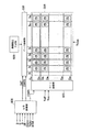
図11は、本発明の他の実施形態による液晶表示装置用薄膜トランジスタ表示板の配置図である。
図11に示す実施形態の薄膜トランジスタ表示板の層状構造はほとんど図6に示した薄膜トランジスタ表示板の層状構造と同様である。
Next, a liquid crystal panel assembly according to another embodiment of the present invention will be described in detail with reference to FIG.
FIG. 11 is a layout view of a thin film transistor array panel for a liquid crystal display according to another embodiment of the present invention.
The layered structure of the thin film transistor array panel of the embodiment shown in FIG. 11 is almost the same as the layered structure of the thin film transistor array panel shown in FIG.
絶縁基板110上に、第1及び第2ゲート電極124a、124b及び端部129a、129bを有する複数の第1及び第2ゲート線121a、121bと、維持電極137及びその延長部139を有する複数の維持電極線131を有するゲート導電体が形成され、その上には、ゲート絶縁膜140が形成されている。ゲート絶縁膜140上には、複数の島状の半導体154a、154b、156a、157aが形成されており、その上には複数の島状オーミック接触部材(図示せず)が形成されている。
A plurality of first and
オーミック接触部材及びゲート絶縁膜140上には、第1及び第2ソース電極173a、173b及び端部179を有する複数のデータ線171と、拡張部177a、177b、端部176a、176b及び接続部176aa、176bbを有する複数の第1及び第2ドレイン電極175a、175bを有するデータ導電体が形成されている。データ導電体171、175a、175b及び露出した第1及び第2半導体154a、154b部分の上には保護膜180が形成されている。保護膜180とゲート絶縁膜140の上にはコンタクトホール181a、181b、182、185a、185bが形成されている。保護膜180の上には、複数の画素電極191、複数の遮蔽電極88及び複数の接触補助部材81a、81b、82が形成されている。
A plurality of
しかし、図6の薄膜トランジスタ表示板と異なり、図11の実施形態では、第2ドレイン電極175bの拡張部177bと、これと重畳する維持電極137の右側部分が図6に示したものより幅が狭いので、第2ストレージキャパシタCSTbの容量が図6に示したものより小さくなる。これにより、第1副画素電極191aに低い電圧が印加され、第2副画素電極191bに高い電圧が印加されるときに第2液晶キャパシタCLCbの容量がより大きくなって、キックバック電圧Vkbがキックバック電圧Vkaより小さくなるのを防ぐ。このように、キックバック電圧Vka、Vkbの大きさを実質的に同一にすることによって、最適の共通電圧Vcomを設定することが容易で、キックバック電圧Vka、Vkbの均衡をとることが可能になるので、画面のフリッカー現象などを防止し、同時に開口率の低下を防止することができる。
図6に示す薄膜トランジスタ表示板の多くの特徴は、図11に示す薄膜トランジスタ表示板にも適用できる。
However, unlike the thin film transistor array panel of FIG. 6, in the embodiment of FIG. 11, the
Many features of the thin film transistor array panel shown in FIG. 6 can be applied to the thin film transistor array panel shown in FIG.
次に、本発明の他の実施形態による液晶表示装置について図12及び図13を参照して詳細に説明する。
図12は、本発明の他の実施形態による液晶表示装置のブロック図であり、図13は、本発明の他の実施形態による液晶表示装置の一つの画素に対する等価回路図である。
本発明の他の実施形態による液晶表示装置は、液晶表示板組立体301とこれに接続されたゲート駆動部403、及びデータ駆動部501、データ駆動部501に接続された階調電圧生成部801、並びにこれらを制御する信号制御部601を備える。
Next, a liquid crystal display device according to another embodiment of the present invention will be described in detail with reference to FIGS.
FIG. 12 is a block diagram of a liquid crystal display device according to another embodiment of the present invention, and FIG. 13 is an equivalent circuit diagram for one pixel of the liquid crystal display device according to another embodiment of the present invention.
A liquid crystal display according to another exemplary embodiment of the present invention includes a liquid crystal
液晶表示板組立体301は、等価回路的に複数の表示信号線(G1−Gn、D1−D2m)と、これに接続されてほぼ行列状に配列された複数の画素PXを備える。
表示信号線(G1−Gn、D1−D2m)は、ゲート信号を伝達する複数のゲート線(G1−Gn)と、データ信号を伝達するデータ線(D1−D2m)を有する。ゲート線(G1−Gn)はほぼ行方向に延びて互いにほぼ平行であり、データ線(D1−D2m)はほぼ列方向に延びて互いにほぼ平行である。一つの画素PXの両側にそれぞれ一対のデータ線(D1−D2m)が配置されている。さらに、表示信号線は、ゲート線(G1−Gn)とデータ線(D1−D2m)以外にもゲート線(G1−Gn)とほぼ平行に延びた維持電極線を有することができる。
The liquid crystal
The display signal lines (G 1 -G n , D 1 -D 2 m ) are a plurality of gate lines (G 1 -G n ) that transmit gate signals and data lines (D 1 -D 2m ) that transmit data signals. Have The gate lines (G 1 -G n ) extend in the row direction and are substantially parallel to each other, and the data lines (D 1 -D 2m ) extend in the column direction and are substantially parallel to each other. A pair of data lines (D 1 -D 2m ) are arranged on both sides of one pixel PX. Further, the display signal line has a storage electrode line extending substantially parallel to the gate line (G 1 -G n ) in addition to the gate line (G 1 -G n ) and the data line (D 1 -D 2m ). Can do.
図13に、表示信号線と一つの画素PXの等価回路が示されているが、図面符号GLで示したゲート線と、図面符号DLa、DLbで示したデータ線以外にも、表示信号線はゲート線GLとほぼ平行に延びた維持電極線SLをさらに有する。
各画素PXは一対の副画素PXc、PXdを有し、各副画素PXc、PXdは、それぞれ当該ゲート線GL及びデータ線DLa、DLbに接続されているスイッチング素子Qc、Qdと、これらに接続された液晶キャパシタCLCc、CLCd及びストレージキャパシタCSTc、CSTdを有する。
FIG. 13 shows an equivalent circuit of the display signal line and one pixel PX. In addition to the gate line indicated by the drawing symbol GL and the data lines indicated by the drawing symbols DLa and DLb, the display signal line includes The storage electrode line SL further extending substantially parallel to the gate line GL.
Each pixel PX has a pair of subpixels PXc and PXd, and each subpixel PXc and PXd is connected to the switching elements Qc and Qd connected to the gate line GL and the data lines DLa and DLb, respectively. Liquid crystal capacitors C LC c and C LC d and storage capacitors C ST c and C ST d.
各副画素PXc、PXdは、図5に示した副画素と実質的に同一であるのでこれに対する詳細な説明は省略する。
階調電圧生成部801は、副画素PXc、PXdの透過率に関連する二組の複数階調電圧を生成する。二組のうちの一組は共通電圧Vcomに対してプラスの値を有し、もう一組はマイナスの値を有する。
Each of the subpixels PXc and PXd is substantially the same as the subpixel shown in FIG.
The gradation
ゲート駆動部403は、液晶表示板組立体301のゲート線(G1−Gn)に接続され、外部からのゲートオン電圧Vonとゲートオフ電圧Voffの組み合わせからなるゲート信号をゲート線(G1−Gn)に印加する。
データ駆動部501は、液晶表示板組立体301のデータ線(D1−D2m)に接続され、階調電圧生成部801からの階調電圧を選択してデータ信号として副画素PXc、PXdに印加する。
信号制御部601は、ゲート駆動部403及びデータ駆動部501などの動作を制御する。
The
The
The
次に、このような液晶表示板組立体301の構造について図14及び図15を参照して詳細に説明する。
図14は、本発明の他の実施形態による液晶表示板組立体の配置図であり、図15は、図14の液晶表示板組立体のXII−XII線に沿った断面図である。
図14及び図15の実施形態による液晶表示板組立体は、薄膜トランジスタ表示板101、共通電極表示板201、及びその間の液晶層3を備える。
Next, the structure of the liquid
FIG. 14 is a layout view of a liquid crystal panel assembly according to another embodiment of the present invention, and FIG. 15 is a cross-sectional view taken along line XII-XII of the liquid crystal panel assembly of FIG.
14 and 15 includes a thin film
まず、薄膜トランジスタ表示板101について詳細に説明する。
透明なガラスまたはプラスチックなどからなる絶縁基板110上に、複数のゲート線121と複数の維持電極線131aを有する複数のゲート導電体が形成されている。
ゲート線121はゲート信号を伝達し、主に横方向に延びている。各ゲート線121は、上方に突出した第1及び第2ゲート電極124c、124dと、他の層または外部駆動回路との接続のために広い面積の端部129を有する。
First, the thin film
A plurality of gate conductors having a plurality of
The
維持電極線131aは、所定の電圧の印加を受けて主に横方向に延びている。各維持電極線131aは、隣接した二つのゲート線121の間に位置し、二つのゲート線121からほぼ同一距離をおいている。各維持電極線131aは、上下に拡張された維持電極137aと維持電極137aから下方に長く延びた棒状の延長部139aを有する。維持電極137aはほぼ長方形で、維持電極線131aに対称であり、延長部139aは第1ゲート電極124cの近傍まで延びている。しかし、維持電極137aを始めとする維持電極線131aの形状及び配置はいろいろな形態に変形可能である。
The
ゲート導電体121、131a上には、SiNxまたはSiOxなどからなるゲート絶縁膜140が形成されている。
ゲート絶縁膜140上には、水素化非晶質シリコンまたは多結晶シリコンなどからなる複数の島状の半導体154c、154d、156b、157bが形成されている。半導体154c、154dは、それぞれ第1及び第2ゲート電極124c、124d上に位置する。半導体156b、157bは、ゲート線121、維持電極線131aの境界を覆う。
A
On the
半導体154c、154d、156b、157b上には、複数の島状のオーミック接触部材163c、163d、165c、165d、166b、167bが形成されている。オーミック接触部材163c−167bは、リンなどのn型不純物が高濃度にドーピングされているn+水素化非晶質シリコンなどの物質からなるか、シリサイドからなることができる。オーミック接触部材163c、165cとオーミック接触部材163d、165dとは、それぞれ対をなして半導体154c、154d上に位置し、オーミック接触部材166b、167bは、それぞれ半導体156b、157b上に位置する。
A plurality of island-shaped
ゲート絶縁膜140及びオーミック接触部材163c、163d、165c、165d、166b、167b上には、複数のデータ線171a、171bと複数対の第1及び第2ドレイン電極175c、175dを有するデータ導電体が形成されている。
データ線171a、171bはデータ信号を伝達し、主に縦方向に延びてゲート線121及び維持電極線131aと交差する。各データ線171a、171bは、第1及び第2ゲート電極124c、124dに向かって延びた複数の第1及び第2ソース電極173c、173dと他の層または外部駆動回路との接続のために広い面積の端部179a、179bを有する。
A data conductor having a plurality of
The
第1及び第2ドレイン電極175c、175dは互いに分離されており、データ線171a、171bとも分離されている。第1及び第2の各ドレイン電極175c、175dは、それぞれのゲート電極124c、124dを中心に第1及び第2ソース電極173c、173dと対向し、一側端に広い面積の長方形状の拡張部177c、177d、棒状の他側の端部176c、176d、並びに拡張部177c、177dと端部176c、176dを接続する接続部176cc、176ddを有する。各拡張部177c、177dは維持電極137aと重畳し、棒状の端部176c、176dは各ゲート電極124c、124dと重畳し、U字状に折曲したソース電極173c、173dで一部覆われている。
The first and
第1ドレイン電極175cの接続部176ccはほとんど維持電極137aの延長部139a上に位置し、維持電極137aの延長部139aと平行に延びてこの延長部139aの縦境界線内に位置する。第2ドレイン電極175dの拡張部177dの面積は、第1ドレイン電極175cの拡張部177cの面積より小さい。
The connection portion 176cc of the
第1及び第2ゲート電極124c、124d、第1及び第2ソース電極173c、173d、並びに第1及び第2ドレイン電極175c、175dは、半導体154c、154dと共に第1及び第2薄膜トランジスタQc、Qdを構成し、薄膜トランジスタQc、Qdのチャンネルは、第1及び第2ソース電極173c、173dと、第1及び第2ドレイン電極175c、175dとの間の半導体154c、154dに形成される。
The first and
オーミック接触部材163c、163d、165c、165d、166b、167bは、その下の半導体154c、154d、156b、157bと、その上のデータ線171a、171b、及び第1、第2ドレイン電極175c、175dとの間にのみ存在し、これらの間の接触抵抗を低くする。島状の半導体154c、154dには、第1及び第2ソース電極173c、173dと第1及び第2ドレイン電極175c、175dとの間を始めとして、これらで覆われず露出した部分がある。半導体156b、157bは、ゲート線121及び維持電極線131a表面のプロファイルを滑らかにして、データ線171a、171b及び第1、第2ドレイン電極175c、175dの断線を防止する。
The
データ線171a、171b、第1、第2ドレイン電極175c、175d及び露出した半導体154c、154d部分上には保護膜180が形成されている。
保護膜180には第1及び第2ドレイン電極175c、175dの拡張部177c、177dとデータ線171a、171bの端部179a、179bをそれぞれ露出させる複数のコンタクトホール185c、185d、182a、182bが形成されており、保護膜180とゲート絶縁膜140には、ゲート線121の端部129を露出させる複数のコンタクトホール181が形成されている。
保護膜180上には、第1及び第2副画素電極191a、191bを有する複数の画素電極191、複数の遮蔽電極88b及び複数の接触補助部材81、82a、82bが形成されている。
A
A plurality of
A plurality of
一つの画素電極191を構成する一対の第1及び第2副画素電極191a、191bはギャップ93を間に挟んで互いに噛み合い、画素電極191の外側境界はほぼ四角形状を有する。第2副画素電極191bは、ほぼ直角に回転した等辺台形で下辺が台形に凹んで、ほとんど第1副画素電極191aで覆われている。第1副画素電極191aは、左側辺で互いに連結されている上部、下部及び中央台形部からなる。第1副画素電極191aの中央台形部は、第2副画素電極191bの凹んだ下辺に嵌合されている。第1副画素電極191aと第2副画素電極191bとの間のギャップ93はほぼ均一な幅を有し、ゲート線121と約45度をなす二対の上部及び下部斜線部と実質的に均一な幅を有する三つの縦部を有する。以下、説明の便宜上、ギャップ93も切開部と称する。
A pair of first and second
第1副画素電極191aは、上部台形部の上側辺及び下部台形部の下側辺から右側辺に向かって延びた切開部96a、96b、97a、97bを有する。また、第1副画素電極191aは、維持電極線131aに沿って延びた切開部91、92aを有し、切開部91、92aは、中央から横方向に延びた横部と、維持電極線131aに対して約45度をなす一対の斜辺を有する。第2副画素電極192bは、左側辺から右側辺に向かって延びた切開部94a、94bを有する。切開部91、92a、94a、94b、96a、96b、97a、97bは、維持電極線131aに対してほぼ反転対称をなしており、これらはゲート線121に対して約45度をなし、互いに垂直に延びている。画素電極191の上半部及び下半部は、切開部91−97bによってそれぞれ8個の領域に分割される。
The
第1及び第2副画素電極191a、191bは、コンタクトホール185c、185dを介して第1及び第2ドレイン電極175c、175dと物理的、電気的に接続されて第1及び第2ドレイン電極175c、175dからデータ電圧の印加を受ける。一対の副画素電極191a、191bには、一つの入力映像信号に対し予め設定された互いに異なるデータ電圧が印加され、その大きさは、第1及び第2副画素電極191a、191bの大きさ及び形状によって設定される。また、第1及び第2副画素電極191a、191bの面積は互いに異なることができる。例えば、第2副画素電極191bは第1副画素電極191aに比較して高い電圧の印加を受け、第1副画素電極191aより面積が小さい。
The first and
データ電圧が印加された第1及び第2副画素電極191a、191bは、共通電圧の印加を受ける共通電極270が第1及び第2液晶キャパシタCLCc、CLCdを構成して第1及び第2薄膜トランジスタQc、Qdが非導通状態になった後も印加された電圧を維持する。各液晶キャパシタCLCc、CLCdは液晶層3部分を誘電体として有する。
The first and
第1及び第2副画素電極191a、191b及びこれと電気的に接続された第1及び第2ドレイン電極175c、175dの拡張部177c、177dは、ゲート絶縁膜140を介在して維持電極137a及び延長部139aを始めとする維持電極線131aと重畳して、第1及び第2液晶キャパシタCLCc、CLCdの電圧維持能力を強化する各ストレージキャパシタCSTc、CSTdを構成する。
The first and
遮蔽電極88bは、共通電圧の印加を受け、データ線171a、171bに沿って延びた縦部と、ゲート線121に沿って延びた横部を有する。縦部はデータ線171a、171bを完全に覆い、横部もゲート線121を完全に覆い、隣接した縦部を接続する。遮蔽電極88bは、データ線171a、171bと画素電極191との間、及びデータ線171a、171bと共通電極270との間に形成される電界を遮断して、画素電極191の電圧歪み及びデータ線171a、171bが伝達するデータ電圧の信号遅延を減少させる。
The
接触補助部材81、82a、82bは、それぞれコンタクトホール181、182a、182bを介してゲート線121の端部129及びデータ線171a、171bの端部179a、179bに接続される。接触補助部材81、82a、82bは、ゲート線121の端部129及びデータ線171a、171bの端部179a、179bと外部装置との接着性を補完し、これらを保護する。
The
次に、共通電極表示板201について詳細に説明する。
透明なガラスまたはプラスチックなどからなる絶縁基板210上に、遮光部材220、複数のカラーフィルタ230、オーバーコート膜250及び共通電極270が順に形成されている。
Next, the
A
共通電極270は、複数組の切開部群71、72、73a、74a、75c、75d、76c、76d、77a、77b、78a、78bを有する。一組の切開部71−78bは、一つの画素電極191と対向し、中央切開部71、72、73a、74a、上部切開部75c、76c、77a、78a及び下部切開部75d、76d、77b、78bを有する。切開部71−78bは、画素電極191の左側辺の中央、画素電極191の切開部91−97bの間、及び周縁切開部97a、97bと画素電極191の角の間に配置されている。また、切開部72−78bは、画素電極191の切開部91−97bと平行に延びた少なくとも一つの斜線部を有する。
The
下部及び上部切開部75c−78bは、ほぼ画素電極191の右側辺から下側または上側辺に向かって延びた斜線部、並びに斜線部の各端から画素電極191の辺に沿って辺と重畳しながら延び、斜線部と鈍角をなす横部及び縦部を有する。
The lower and
中央切開部71は、画素電極191の左側辺に沿って左側辺と重畳しながら延びた縦部と、縦部の中央で維持電極線131aに沿って延びた横部を有する。中央切開部72、73aは、ほぼ維持電極線131aに沿って延びた横部と、これから維持電極線131aと斜角をなして画素電極191の左側辺に向かって延びた一対の斜線部と、斜線部の各端から画素電極191の左側辺に沿って左側辺と重畳しながら延び、斜線部と鈍角をなす縦断縦部を有する。中央切開部74aは、画素電極191の右側辺に沿って右側辺と重畳しながら延びた縦部、縦部の各端から画素電極191の左側辺に向かって延びた一対の斜線部、並びに斜線部の各端から第2副画素電極191bの左側辺に沿って左側辺と重畳しながら延び、斜線部と鈍角をなす縦断縦部を有する。
The
切開部72−77bの斜線部には三角形状のノッチが形成されている。このノッチは、四角形、台形または半円形に形成されたり、突出した形状や凹んだ形状に形成されたりすることもできる。
下部及び上部表示板101、201の内側面には配向膜11、21が塗布されており、外側面には偏光子を有する偏光板12、22が備えられている。
図14及び図15に示す実施形態による液晶表示装置の表示動作は、前記実施形態と実質的に同一であるのでこれに対する説明は省略する。
A triangular notch is formed in the hatched portion of the incision 72-77b. The notch can be formed in a square shape, a trapezoidal shape or a semicircular shape, or can be formed in a protruding shape or a recessed shape.
Since the display operation of the liquid crystal display device according to the embodiment shown in FIGS. 14 and 15 is substantially the same as that of the above embodiment, the description thereof will be omitted.
図14及び図15に示す実施形態の液晶表示装置においても、第1及び第2副画素PXc、PXdのキックバック電圧Vkc、Vkdの大きさは実質的に同一である。第1及び第2液晶キャパシタCLCc、CLCdの容量は、第1及び第2副画素電極191a、191bの面積などによって決定されており、第1及び第2副画素電極191a、191bに実質的に同一電圧が印加されるときに、第1副画素電極191aが第2副画素電極191bより面積が大きいため、第1液晶キャパシタCLCcが第2液晶キャパシタCLCdより容量が大きい。また、維持電極137aと重畳する第1ドレイン電極175cの拡張部177cが第2ドレイン電極175dの拡張部177dより面積が大きい。ところが、ほとんど低階調で動作する第1副画素電極191aの第1液晶キャパシタCLCcは、液晶の配列による誘電率が第2副画素電極191bの誘電率に比較して小さく、この第1液晶キャパシタCLCcの容量もより小さくなるので、ほとんど高階調で動作する第2副画素電極191bの第2液晶キャパシタCLCdの容量はより大きくなる。これにより、各ストレージキャパシタCSTc、CSTdの容量を固定すれば、第1副画素電極191aへのキックバック電圧Vkcが第2副画素電極191bへのキックバック電圧Vkdより大きくなる。よって、キックバック電圧Vkc、Vkdの均衡をとるために、第1及び第2ストレージキャパシタCSTc、CSTdの値を調整する必要がある。
Also in the liquid crystal display device of the embodiment shown in FIGS. 14 and 15, the magnitudes of the kickback voltages Vkc and Vkd of the first and second subpixels PXc and PXd are substantially the same. The capacities of the first and second liquid crystal capacitors C LC c and C LC d are determined by the areas of the first and
第1ストレージキャパシタCSTcの容量を大きくしてキックバック電圧Vkcが高くなるのを防止するために、第1ドレイン電極175cの接続部176ccと重畳する維持電極137aの延長部139aをさらに設けたり、第1ドレイン電極175cの拡張部177c及びこれと重畳する維持電極137aの縦幅をより大きくしたりする。このように、第1及び第2副画素PXc、PXdのキックバック電圧Vkc、Vkdの大きさを実質的に同一にすることによって、最適の共通電圧Vcomを設定することが容易で、キックバック電圧Vkc、Vkdの均衡をとることが可能になるので、画面のフリッカー現象などを防止することができる。
To prevent by increasing the capacity of the first storage capacitor C ST c is the kickback voltage Vkc higher, or further provided with an
特に、図14及び図15に示すように、第1ドレイン電極175cの接続部176ccと重畳する維持電極137aの延長部139aをさらに設けることでストレージキャパシタCSTaを形成できるので、維持電極137aの面積を減少させても充分な保持容量を確保でき、同時に開口率を増加させることができる。
In particular, as shown in FIGS. 14 and 15, it is possible to form a storage capacitor C ST a by further providing the
また、本実施形態においても、第2ドレイン電極175dの拡張部177dと、これと重畳する維持電極137aの右側部分の幅をより狭くして、第2ストレージキャパシタCSTdの容量をより小さくすることによって、第2副画素電極191bに高い電圧が印加されるときに、キックバック電圧Vkdが小さくなるのを補償することができる。この結果、キックバック電圧Vkc、Vkdの均衡をとることができるので、フリッカー現象を防止し、同時に開口率の減少を防止することができる。
図1乃至図10の液晶表示板組立体の多くの特徴は、図12乃至図115の液晶表示板組立体にも適用できる。
Also in the present embodiment, the width of the
Many features of the liquid crystal panel assembly of FIGS. 1 to 10 can be applied to the liquid crystal panel assembly of FIGS.
次に、図16及び図17を参照して本発明の他の実施形態による液晶表示装置用薄膜トランジスタについて詳細に説明する。
図16は、本発明の他の実施形態による液晶表示装置用薄膜トランジスタ表示板の配置図であり、図17は、図16の液晶表示装置用薄膜トランジスタ表示板のXIIIB−XIIIB線に沿った断面図である。
Next, a thin film transistor for a liquid crystal display according to another embodiment of the present invention will be described in detail with reference to FIGS.
16 is a layout view of a thin film transistor array panel for a liquid crystal display according to another embodiment of the present invention, and FIG. 17 is a cross-sectional view taken along line XIIIB-XIIIB of the thin film transistor array panel for a liquid crystal display of FIG. is there.
透明なガラスまたはプラスチックなどからなる絶縁基板110上に、複数のゲート線121と複数の維持電極線131bが形成されている。
ゲート線121はゲート信号を伝達し、主に横方向に延びている。各ゲート線121は、上方に突出した複数のゲート電極124eと他の層または外部駆動回路との接続のために広い面積の端部129を有する。
A plurality of
The
維持電極線131bは所定の電圧の印加を受け、主に横方向に延びている。各維持電極線131bは、隣接した二つのゲート線121の間に位置し、二つのゲート線121からほぼ同一距離をおいている。各維持電極線131bは、上下に拡張された維持電極137bと、維持電極137bから下方に長く延びた棒状の延長部139bを有する。維持電極137bはほぼ長方形で、維持電極線131bに対称であり、延長部139bはゲート電極124eの近傍まで延びている。しかし、維持電極137bを始めとする維持電極線131bの形状及び配置は様々な形態に変形することができる。
The
ゲート線121及び維持電極線131b上には、SiNxまたはSiOxなどからなるゲート絶縁膜140が形成されている。
ゲート絶縁膜140上には、水素化非晶質シリコンまたは多結晶シリコンなどからなる複数の島状の半導体154eが形成されている。半導体154eは、それぞれゲート電極124e上に位置する。半導体154eは、ゲート線121境界まで延びており、維持電極線131bの境界にも配置できる。半導体154eの上には複数の島状オーミック接触部材163e、165eが形成されている。オーミック接触部材163e、165eは対をなして半導体154e上に位置する。
A
On the
ゲート絶縁膜140及びオーミック接触部材163e、165e上には、複数のデータ線171と複数のドレイン電極175eが形成されている。
データ線171はデータ信号を伝達し、主に縦方向に延びてゲート線121及び維持電極線131bと交差する。各データ線171は、ゲート電極124eに向かって延びた複数のソース電極173eと、他の層または外部駆動回路との接続のために広い面積の端部179を有する。
A plurality of
The
ドレイン電極175eは、データ線171と分離されている。各ドレイン電極175eは、ゲート電極124eを中心にソース電極173eと対向し、一側端に面積が広い長方形状の拡張部177e、棒状の他側の端部176e、並びに拡張部177eと端部176eを接続する接続部176eeを有する。
各拡張部177eは維持電極137bと重畳し、棒状の端部176eはゲート電極124eと重畳し、U字状に折曲したソース電極173eで一部覆われている。以下、拡張部177eを結合電極と称する。
The
Each
ドレイン電極175eの接続部176eeは、ほとんど維持電極137bの延長部139b上に位置し、維持電極137bの延長部139bと平行に延びてこの延長部139bの縦境界線内に位置する。
一つのゲート電極124e、一つのソース電極173e及び一つのドレイン電極175eは、半導体154eと共に一つの薄膜トランジスタを構成し、薄膜トランジスタのチャンネルは、ソース電極173eとドレイン電極175eとの間の半導体154eに形成される。
The connection part 176ee of the
One
オーミック接触部材163e、165eは、その下の半導体154eと、その上のデータ線171及びドレイン電極175eとの間にのみ存在し、これらの間の接触抵抗を低くする。島状の半導体154eにはソース電極173eとドレイン電極175eとの間を始めとして、これらで覆われず露出した部分がある。半導体154eの延長部は、ゲート線121表面のプロファイルを滑らかにしてデータ線171の断線を防止する。
The
データ線171、ドレイン電極175e及び露出した半導体154e部分の上には保護膜180が形成されている。
保護膜180には結合電極177eとデータ線171の端部179をそれぞれ露出させる複数のコンタクトホール182、185eが形成されており、保護膜180とゲート絶縁膜140にはゲート線121の端部129を露出させる複数のコンタクトホール181が形成されている。
A
A plurality of
保護膜180上には、複数の画素電極191、複数の遮蔽電極88及び複数の接触補助部材81、82が形成されている。
各画素電極191は、4つの角が面取りされたほぼ四角形状を有し、面取りされた斜辺はゲート線121に対して約45度の角度をなす。画素電極191はゲート線121と重畳し、このため開口率を大きくすることができる。
A plurality of
Each
各画素電極191は、ギャップ93を間に挟んで分かれた一対の第1及び第2副画素電極191c、191dを有する。ギャップ93は、画素電極191の左側辺から右側辺に延びている上部及び下部斜線部と、これらを連結する縦部を有する。ギャップ93の上部及び下部斜線部は、ゲート線121と約45度をなし、互いに垂直である。
よって、第2副画素電極191dは、ほぼ直角に回転した二等辺台形状を有し、第1副画素電極191cは第2副画素電極191dの斜辺と対向し、ほぼ直角に回転した一対の台形部と第2副画素電極191dの右側辺と対向する縦部を有する。
Each
Accordingly, the
第1副画素電極191cは、下部及び上部切開部94a、94b、95a、95bを有する。下部及び上部切開部94a、94bは、第1副画素電極191cの下側または上側の角から右側辺に斜めに延びており、下部及び上部切開部95a、95bは、第1副画素電極191cの下側辺または上側辺から右側辺に斜めに延びている。下部及び上部切開部94a、94b、95a、95bは、ゲート線121に対して約45度の角度をなし、互いに垂直に延びている。
The
第2副画素電極191dは中央切開部91、92を有する。中央切開部91は、第2副画素電極191dの左側辺の中央に入口を有し、切開部91の入口は、ギャップ93の上部斜線部及び下部斜線部とそれぞれ実質的に平行な一対の斜辺を有している。切開部92は、維持電極137bの中央に横に短く延びた横部と、これからギャップ93の上部斜線部及び下部斜線部とほぼ平行に延びた一対の斜線部を有する。以下、説明の便宜上、ギャップ93も切開部と称する。
The
画素電極191は、上記切開部91、92、93、94a、94b、95a、95bによって複数の領域に分割される。切開部91、92、93、94a、94b、95a、95bは維持電極線131bに対してほぼ反転対称をなす。
この時、切開部の数または領域の数は、画素電極191の大きさ、画素電極191の横辺と縦辺の長さ比、液晶層の種類や特性など、設計要素によって異なる。
下部表示板100の外部面には偏光子を有する偏光板12が備えられている。
The
At this time, the number of incisions or the number of regions varies depending on design factors such as the size of the
A
第1副画素電極191cはコンタクトホール185eを介してドレイン電極175eと物理的、電気的に接続されてドレイン電極175eからデータ電圧の印加を受ける。第1及び第2副画素電極191c、191dと共通電極(図示せず)は、第1及び第2液晶キャパシタCLCe、CLCfを構成して、薄膜トランジスタが非導通状態になった後も印加された電圧を維持する。
The
第1副画素電極191c及びこれに接続された結合電極177eは、維持電極137bを始めとする維持電極線131bと重畳してストレージキャパシタCSTeを構成し、ストレージキャパシタCSTeは、第1液晶キャパシタCLCeの電圧維持能力を強化する。
第2副画素電極191dは結合電極177eと重畳して結合キャパシタCcp(図示せず)を構成する。
The first
The
薄膜トランジスタは、ゲート線121からのゲート信号に従ってデータ線171からのデータ電圧を第1液晶キャパシタCLCe及び結合キャパシタCcpに印加し、結合キャパシタCcpは該電圧をその大きさを変えて第2液晶キャパシタCLCfに伝達する。
The thin film transistor applies the data voltage from the
維持電極線131bに共通電圧Vcomが印加され、キャパシタCLCe、CSTe、CLCf、Ccpと、その静電容量を同一図面符号で示すと、第1液晶キャパシタCLCeに充電された電圧Veと、第2液晶キャパシタCLCfに充電された電圧Vfは、次のような関係を有する。
Vf=Ve×[Ccp/(Ccp+CLCf)]
Ccp/(Ccp+CLCf)の値が1より小さいので、第2液晶キャパシタCLCfに充電された電圧Vfは、第1液晶キャパシタCLCeに充電された電圧Veに比べて常に小さい。この関係は、維持電極線131bの電圧が共通電圧Vcomでない場合にも同様に成立する。
The common voltage Vcom is applied to the
Vf = Ve × [Ccp / (Ccp + C LC f)]
Since the value of Ccp / (Ccp + C LC f) is smaller than 1, the voltage Vf charged in the second liquid crystal capacitor C LC f is always smaller than the voltage Ve charged in the first liquid crystal capacitor C LC e. This relationship is similarly established when the voltage of the
このように、第1または第2液晶キャパシタCLCe、CLCfの両端に電位差が生じれば、下部表示板100と共通電極表示板(図示せず)の面にほぼ垂直な電場が液晶層に生成され、液晶分子は電場に応答してその長軸が電場の方向に垂直をなすように傾斜し、液晶分子が傾いた程度によって液晶層に入射した光の偏光の変化程度が変化する。このような偏光の変化は、偏光子を有する偏光板12によって透過率の変化として現れ、これによって液晶表示装置は映像を表示する。
As described above, when a potential difference occurs between both ends of the first or second liquid crystal capacitors C LC e and C LC f, an electric field substantially perpendicular to the surfaces of the
液晶分子の傾斜角度は電場の強さによって変わり、第1液晶キャパシタCLCeの電圧Veと第2液晶キャパシタCLCfの電圧Vfが互いに異なるので、第1副画素と第2副画素で液晶分子の傾斜角度が異なり、このため二つの副画素の輝度が異なる。これにより、第1液晶キャパシタCLCeの電圧Veと第2液晶キャパシタCLCfの電圧Vfを適切に調整すれば、側面から見る映像が正面から見る映像に最大限に近接することができ、この結果、側面視認性を向上させることができる。 The tilt angle of the liquid crystal molecules varies depending on the intensity of the electric field, and the voltage Ve of the first liquid crystal capacitor C LC e and the voltage V f of the second liquid crystal capacitor C LC f are different from each other. The tilt angles of the molecules are different, so that the brightness of the two subpixels is different. Accordingly, if the voltage Ve of the first liquid crystal capacitor C LC e and the voltage V f of the second liquid crystal capacitor C LC f are appropriately adjusted, the image viewed from the side surface can be as close as possible to the image viewed from the front surface, As a result, side visibility can be improved.
遮蔽電極88は共通電圧の印加を受け、データ線171に沿って延びた縦部とゲート線121に沿って延びて隣接した縦部を連結する横部を有する。縦部はデータ線171を完全に覆い、横部はゲート線121の境界の内側に位置する。
接触補助部材81、82は、それぞれコンタクトホール181、182を介してゲート線121の端部129及びデータ線171の端部179に接続される。
The
The
このように、図16及び図17に示すように、ドレイン電極175eの接続部176eeと重畳する維持電極137bの延長部139bをさらに設けてストレージキャパシタCSTeを形成できるので、維持電極137bの面積を減らしても充分な保持容量を確保でき、同時に開口率を増加させることができる。
図1乃至図10に示した液晶表示板組立体の多くの特徴は、図16及び図17の液晶表示装置用薄膜トランジスタ表示板にも適用できる。
Thus, as shown in FIGS. 16 and 17, the storage capacitor C ST e can be formed by further providing the
Many features of the liquid crystal display panel assembly shown in FIGS. 1 to 10 can be applied to the thin film transistor array panel for the liquid crystal display of FIGS.
最後に、図18及び図19を参照して本発明の他の実施形態による液晶表示装置用薄膜トランジスタについて詳細に説明する。
図18は、本発明の他の実施形態による液晶表示装置用薄膜トランジスタ表示板の配置図であり、図19は、図18の液晶表示装置用薄膜トランジスタ表示板のXIVB−XIVB線に沿った断面図である。
図18及び図19に示す実施形態による薄膜トランジスタ表示板の層状構造は、図116及び図17に示した薄膜トランジスタ表示板の層状構造とほとんど同様である。
Finally, a thin film transistor for a liquid crystal display according to another embodiment of the present invention will be described in detail with reference to FIGS.
18 is a layout view of a thin film transistor array panel for a liquid crystal display according to another embodiment of the present invention, and FIG. 19 is a cross-sectional view taken along the line XIVB-XIVB of the thin film transistor array panel for the liquid crystal display of FIG. is there.
The layered structure of the thin film transistor array panel according to the embodiment shown in FIGS. 18 and 19 is almost the same as the layered structure of the thin film transistor array panel shown in FIGS.
絶縁基板110上に、ゲート電極124e及び端部129を有する複数のゲート線121と、維持電極137b及び延長部139bを有する複数の維持電極線131bが形成されており、その上には、ゲート絶縁膜140が形成されている。ゲート絶縁膜140上には、複数の島状の半導体154eが形成されており、その上には、複数の島状のオーミック接触部材163e、165eが形成されている。ゲート絶縁膜140及びオーミック接触部材163e、165e上には、ソース電極173e及び端部179を有する複数のデータ線171と、拡張部177e、端部176e及び接続部176eeを有する複数のドレイン電極175eが形成されている。データ線171、ドレイン電極175e及び露出した半導体154e部分の上には、コンタクトホール181、182、185を有する保護膜180が形成されており、その上には、複数の画素電極191、複数の遮蔽電極88、及び複数の接触補助部材81、82が形成されている。下部表示板100の底面には偏光子を有する偏光板12が備えられている。
On the insulating
しかし、図16及び図17に示した薄膜トランジスタ表示板と異なり、図18及び図19に示す実施形態では各画素電極191は分離されておらず、中央切開部91、92、下部切開部93a、94a、95a及び上部切開部93b、94b、95bを有する。
However, unlike the thin film transistor array panel shown in FIGS. 16 and 17, the
下部及び上部切開部93a、93b、94a、94bは、画素電極191cの左側辺から右側辺に斜めに延びており、下部及び上部切開部95a、95bは、画素電極191の下側辺または上側辺から右側辺に斜めに延びている。下部及び上部切開部93a、93b、94a、94b、95a、95bは、ゲート線121に対して約45度の角度をなし、互いに垂直に延びている。
The lower and
中央切開部91は、画素電極191の左側辺の中央に入口を有し、切開部91の入口は、下部及び上部切開部93a−95bとそれぞれ実質的に平行な一対の斜辺を有している。切開部92は、維持電極137bの中央に横に短く延びた横部と、これからギャップ93の上部斜線部及び下部斜線部とほぼ平行に延びた一対の斜線部を有する。
これにより、画素電極191は、切開部91、92、93a、93b、94a、94b、95a、95bによって複数の領域に分割される。切開部91−95bは、維持電極線131bに対しほぼ反転対称をなす。
The
As a result, the
画素電極191は、コンタクトホール185を介してドレイン電極175eと物理的、電気的に接続されてドレイン電極175eからデータ電圧の印加を受け、共通電極(図示せず)と共に液晶キャパシタCLCgを構成して、薄膜トランジスタが非導通状態になった後も印加された電圧を維持する。
The
画素電極191及びこれに接続されたドレイン電極の拡張部177eは、維持電極137bを始めとする維持電極線131bと重畳してストレージキャパシタCSTgを構成し、ストレージキャパシタCSTgは、液晶キャパシタCLCgの電圧維持能力を強化する。
薄膜トランジスタがゲート線121からのゲート信号に従ってデータ線171からのデータ電圧を液晶キャパシタCLCgに印加すれば、液晶層(図示せず)の液晶分子は、液晶キャパシタCLCgの電場に応答して、その長軸が電場の方向に垂直をなすように傾き、液晶分子が傾く程度によって液晶層に入射した光の偏光の変化程度が変化する。このような偏光の変化は、偏光子を有する偏光板12によって透過率の変化として現れ、これによって液晶表示装置は映像を表示する。
If the thin film transistor applies the data voltage from the
液晶分子の傾斜方向は、画素電極191の切開部91−95bと共通電極(図示せず)の切開部(図示せず)が電場を歪曲して形成する水平成分によって決定され、この電場の水平成分は、切開部91−95bの辺と画素電極191の辺に垂直である。図18に示すように、液晶分子の傾斜方向は約4つの方向である。このように、液晶分子の傾斜方向を複数にすることによって液晶表示装置の基準視野角を大きくすることができる。
液晶分子の傾斜方向を決定するための切開部91−95bの形状及び配置は変更することができ、少なくとも一つの切開部91−95bは突起(図示せず)や陥没部(図示せず)で代替することができる。突起は有機物または無機物からなることができ、電場生成電極の上または下に配置できる。
The inclination direction of the liquid crystal molecules is determined by a horizontal component formed by distorting the electric field by the incision 91-95b of the
The shape and arrangement of the incisions 91-95b for determining the tilt direction of the liquid crystal molecules can be changed, and at least one incision 91-95b is a protrusion (not shown) or a depression (not shown). Can be substituted. The protrusion may be made of an organic material or an inorganic material, and may be disposed on or below the electric field generating electrode.
上述の実施形態においても、図18及び図19に示すように、ドレイン電極175eの接続部176eeと重畳する維持電極137bの延長部139bをさらに設けてストレージキャパシタCSTgを形成できるので、維持電極137bの面積を減らしても充分な保持容量を確保でき、同時に開口率を増加させることができる。
図1乃至図10の液晶表示板組立体の多くの特徴は、図18及び図19の液晶表示装置用薄膜トランジスタ表示板にも適用できる。
In the embodiments described above, as shown in FIGS. 18 and 19, it is possible to form a storage capacitor C ST g further provided an
Many features of the liquid crystal panel assembly of FIGS. 1 to 10 can be applied to the thin film transistor array panel for the liquid crystal display device of FIGS.
一方、図6乃至図10のように、ドレイン電極175aの接続部176aa下に維持電極137の延長部139をさらに設けてストレージキャパシタCSTaを形成し、維持電極137の面積を減らして開口率を増加させる構造は、スイッチング素子を一つまたは複数個備えた表示板など、他の構造を有する表示板にも適用できる。
On the other hand, as shown in FIGS. 6-10, to form a storage capacitor C ST a further provided an
以上、本発明の好ましい実施形態について詳細に説明したが、本発明の権利範囲はこれに限定されず、請求の範囲で定義している本発明の基本概念を利用した当業者の多様な変形及び改良形態も本発明の権利範囲に属するものである。 The preferred embodiments of the present invention have been described in detail above, but the scope of the present invention is not limited thereto, and various modifications and variations of those skilled in the art using the basic concept of the present invention defined in the claims. Improvements are also within the scope of the present invention.
3 液晶層
12、22 偏光板
11、21 配向膜
71、72、73、73a、74a(図14、15)、 共通電極の中央切開部
74a(図7〜9)、75a、75c、76a、76c、77a、78a 共通電極の上部切開部
74b、75b、75d、76b、76d、77b、78b 共通電極の下部切開部
81、81a、81b、82、82a、82b 接触補助部材
88、88b 遮蔽電極
91、92(図16〜19)、92a 画素電極の中央切開部
92(図6、8、9、11)、93 画素電極のギャップ(切開部)
93a(図6、8、9、11)、93b、94a(図6、8、9、11、14、15)、94b、95b、96a、97a、 画素電極の上部切開部
93a(図18、19)、93c、94a(図16〜19)、94c、95a、96b、97b 画素電極の下部切開部
100、101 下部表示板(薄膜トランジスタ表示板)
110、210 基板(絶縁基板)
121 ゲート線(ゲート導電体)
121a 第1ゲート線(ゲート導電体)
121b 第2ゲート線(ゲート導電体)
124a、124c 第1ゲート電極
124b、124d 第2ゲート電極
124e ゲート電極
129 ゲート線の端部
129a 第1ゲート線の端部
129b 第2ゲート線の端部
131、131a、131b 維持電極線(ゲート導電体)
137、137a、137b 維持電極
139、139a、139b 維持電極の延長部
140 ゲート絶縁膜
154a 第1半導体
154b 第2半導体
154c、154d、154e、156a、156b、157a、157b 半導体
163a、163b、163c、163d、163e、165a、165b、165c、165d、165e、166a、166b、167b オーミック接触部材
171、171a、171b データ線(データ導電体)
173a、173c 第1ソース電極
173b、173d 第2ソース電極
173e ソース電極
175a、175c 第1ドレイン電極(データ導電体)
175b、175d 第2ドレイン電極(データ導電体)
175e ドレイン電極
176a、176c 第1ドレイン電極の端部
176b、176d 第2ドレイン電極の端部
176e ドレイン電極の端部
176aa、176cc 第1ドレイン電極の接続部
176bb、176dd 第2ドレイン電極の接続部
176ee ドレイン電極の接続部
177a、177c 第1ドレイン電極の拡張部(電極)
177b、177d 第2ドレイン電極の拡張部(電極)
177e、 ドレイン電極の拡張部(結合電極)
179、179a、179b データ線の端部
180 保護膜
181、181a、181b、182、182a、182b、185、185a、185b、185c、185d、185e コンタクトホール
191 画素電極(電場生成電極)
191a、191c 第1副画素電極
191b、191d 第2副画素電極
200、201 上部表示板(共通電極表示板)
220 遮光部材
225 遮光部材の開口部
230 カラーフィルタ
250 オーバーコート膜
270 共通電極(電場生成電極)
300、301 液晶表示板組立体
400、400a、400b、403 ゲート駆動部
500、501 データ駆動部
600、601 信号制御部
800、801 階調電圧生成部
3
93a (FIGS. 6, 8, 9, 11), 93b, 94a (FIGS. 6, 8, 9, 11, 14, 15), 94b, 95b, 96a, 97a, an upper cut-out
110, 210 substrate (insulating substrate)
121 Gate line (gate conductor)
121a First gate line (gate conductor)
121b Second gate line (gate conductor)
124a, 124c
137, 137a, 137b Sustain
173a, 173c
175b, 175d Second drain electrode (data conductor)
175e Drain electrode 176a, 176c End of
177b, 177d Second drain electrode extension (electrode)
177e, drain electrode extension (coupled electrode)
179, 179a, 179b End of
191a, 191c
220 Light-shielding
300, 301 Liquid crystal
Claims (20)
前記基板上に形成され、前記第1ゲート電極と分離されている維持電極と、
前記第1ゲート電極及び前記維持電極上に形成されるゲート絶縁膜と、
前記ゲート絶縁膜上に形成される第1半導体と、
前記第1半導体上に形成される第1ソース電極と、
前記第1半導体層上に形成され、前記第1ソース電極と分離され、前記第1ゲート電極と重畳する端部、前記維持電極と重畳して該端部と離れている拡張部、及び該端部と該拡張部を接続する接続部を有する第1ドレイン電極と、
前記第1ソース電極及び第1ドレイン電極上に形成され、前記第1ドレイン電極の拡張部を露出させるコンタクトホールを有する保護膜と、
前記コンタクトホールを介して前記第1ドレイン電極に接続される第1電場生成電極とを備え、
前記維持電極は、前記第1ドレイン電極の拡張部と重畳する本体部と、前記第1ドレイン電極の接続部と重畳する延長部と、を有することを特徴とする液晶表示装置。 A first gate electrode formed on the substrate;
A sustain electrode formed on the substrate and separated from the first gate electrode;
A gate insulating film formed on the first gate electrode and the sustain electrode;
A first semiconductor formed on the gate insulating film;
A first source electrode formed on the first semiconductor;
An end portion formed on the first semiconductor layer, separated from the first source electrode and overlapping the first gate electrode; an extension portion overlapping the sustain electrode and separated from the end portion; and the end A first drain electrode having a connection portion connecting the portion and the extension portion;
A protective film having a contact hole formed on the first source electrode and the first drain electrode and exposing an extension of the first drain electrode;
A first electric field generating electrode connected to the first drain electrode through the contact hole,
The liquid crystal display device, wherein the sustain electrode includes a main body that overlaps with an extension of the first drain electrode, and an extension that overlaps with a connection of the first drain electrode.
前記ゲート絶縁膜上に形成される第2半導体と、
前記第2半導体上に形成される第2ソース電極と、
前記第2半導体上に形成され、前記第2ソース電極と分離され、前記第2電場生成電極に接続される第2ドレイン電極とをさらに備え、
前記第1電場生成電極と前記第2電場生成電極とは、一つの映像情報から得られた互いに異なる大きさのデータ電圧の印加を受けることを特徴とする請求項4に記載の液晶表示装置。 A second gate electrode formed on the substrate;
A second semiconductor formed on the gate insulating film;
A second source electrode formed on the second semiconductor;
A second drain electrode formed on the second semiconductor, separated from the second source electrode, and connected to the second electric field generating electrode;
5. The liquid crystal display device according to claim 4, wherein the first electric field generating electrode and the second electric field generating electrode are applied with data voltages of different magnitudes obtained from one video information. 6.
前記第2ゲート電極に接続される第2ゲート線と、
前記第1及び第2ソース電極に接続されるデータ線とをさらに備えることを特徴とする請求項6に記載の液晶表示装置。 A first gate line connected to the first gate electrode;
A second gate line connected to the second gate electrode;
The liquid crystal display device according to claim 6, further comprising a data line connected to the first and second source electrodes.
前記第1ソース電極に接続される第1データ線と、
前記第2ソース電極に接続される第2データ線とをさらに備えることを特徴とする請求項6に記載の液晶表示装置。 A gate line connected to the first and second gate electrodes;
A first data line connected to the first source electrode;
The liquid crystal display device according to claim 6, further comprising a second data line connected to the second source electrode.
前記第1及び第2副画素に接続される複数の第1信号線と、
前記第1信号線と交差し第1副画素に接続される第2信号線と、
前記第1信号線と交差し第2副画素に接続される第3信号線とを備え、
前記第1副画素は、前記第1及び第2信号線に接続される第1スイッチング素子、及び該第1スイッチング素子に接続される第1液晶キャパシタと第1ストレージキャパシタとを有し、
前記第2副画素は、前記第1及び第3信号線に接続される第2スイッチング素子、及び該第2スイッチング素子に接続される第2液晶キャパシタと第2ストレージキャパシタとを有し、
前記第1及び第2液晶キャパシタに印加される電圧は一つの映像情報から得られ、
前記第1副画素には所定の電圧に対し前記第2副画素より低い電圧が印加され、
前記第1及び第2副画素に同一電圧が印加されるときに、前記第1及び第2副画素のキックバック電圧の大きさを実質的に同一にする第1及び第2ストレージキャパシタの静電容量を各々第1及び第2容量とする場合、
前記第1ストレージキャパシタの静電容量が前記第1容量より大きいか、前記第2ストレージキャパシタの容量が前記第2容量より小さいことを特徴とする液晶表示装置。 A plurality of pixels arranged in a matrix and having first and second subpixels;
A plurality of first signal lines connected to the first and second subpixels;
A second signal line crossing the first signal line and connected to the first subpixel;
A third signal line crossing the first signal line and connected to the second subpixel,
The first sub-pixel includes a first switching element connected to the first and second signal lines, a first liquid crystal capacitor connected to the first switching element, and a first storage capacitor,
The second subpixel includes a second switching element connected to the first and third signal lines, a second liquid crystal capacitor connected to the second switching element, and a second storage capacitor,
The voltage applied to the first and second liquid crystal capacitors is obtained from one piece of video information,
A voltage lower than the second subpixel is applied to the first subpixel with respect to a predetermined voltage,
When the same voltage is applied to the first and second subpixels, the electrostatic capacitances of the first and second storage capacitors that make the magnitudes of the kickback voltages of the first and second subpixels substantially the same. When the capacities are first and second capacities, respectively,
The liquid crystal display device, wherein the capacitance of the first storage capacitor is larger than the first capacitance or the capacitance of the second storage capacitor is smaller than the second capacitance.
前記第2スイッチング素子は第2ゲート電極と第2ドレイン電極とを有し、
前記第1及び第2ストレージキャパシタは、前記第1及び第2ゲート電極と分離され、本体部とこれから分岐した延長部を有する維持電極を共通に有し、
前記第1ストレージキャパシタは前記維持電極と前記第1ドレイン電極との重畳からなり、
前記第2ストレージキャパシタは前記維持電極と前記第2ドレイン電極との重畳からなり、
前記第1液晶キャパシタは前記第1スイッチング素子に接続される第1副画素電極を有し、
前記第2液晶キャパシタは前記第2スイッチング素子に接続される第2副画素電極を有することを特徴とする請求項15に記載の液晶表示装置。 The first switching element has a first gate electrode and a first drain electrode,
The second switching element has a second gate electrode and a second drain electrode,
The first and second storage capacitors have a sustain electrode that is separated from the first and second gate electrodes and has a main body portion and an extension portion branched therefrom,
The first storage capacitor comprises a superposition of the sustain electrode and the first drain electrode,
The second storage capacitor comprises a superposition of the sustain electrode and the second drain electrode,
The first liquid crystal capacitor has a first subpixel electrode connected to the first switching element,
The liquid crystal display device according to claim 15, wherein the second liquid crystal capacitor has a second subpixel electrode connected to the second switching element.
前記維持電極の本体部は、前記第1ドレイン電極の拡張部及び前記第2ドレイン電極と重畳し、
前記維持電極の延長部は、前記第1ドレイン電極の接続部と重畳することを特徴とする請求項16に記載の液晶表示装置。 The first drain electrode has an end portion that overlaps the first gate electrode, an extension portion that overlaps the sustain electrode and is separated from the end portion, and a connection portion that connects the end portion and the extension portion. ,
The main body of the sustain electrode overlaps with the extended portion of the first drain electrode and the second drain electrode,
The liquid crystal display device of claim 16, wherein the extended portion of the sustain electrode overlaps with the connection portion of the first drain electrode.
前記維持電極と前記第1ドレイン電極とが重畳する面積は、前記維持電極と前記第2ドレイン電極とが重畳する面積より大きいことを特徴とする請求項16に記載の液晶表示装置。 The area of the first subpixel electrode is larger than the area of the second subpixel electrode,
The liquid crystal display device according to claim 16, wherein an area where the sustain electrode and the first drain electrode overlap is larger than an area where the sustain electrode and the second drain electrode overlap.
Applications Claiming Priority (2)
| Application Number | Priority Date | Filing Date | Title |
|---|---|---|---|
| KR10-2005-0046911 | 2005-06-01 | ||
| KR1020050046911A KR101160831B1 (en) | 2005-06-01 | 2005-06-01 | Liquid crystal display |
Publications (2)
| Publication Number | Publication Date |
|---|---|
| JP2006338024A true JP2006338024A (en) | 2006-12-14 |
| JP5391435B2 JP5391435B2 (en) | 2014-01-15 |
Family
ID=37493634
Family Applications (1)
| Application Number | Title | Priority Date | Filing Date |
|---|---|---|---|
| JP2006154072A Active JP5391435B2 (en) | 2005-06-01 | 2006-06-01 | Liquid crystal display |
Country Status (4)
| Country | Link |
|---|---|
| US (2) | US7956942B2 (en) |
| JP (1) | JP5391435B2 (en) |
| KR (1) | KR101160831B1 (en) |
| CN (1) | CN1892391B (en) |
Cited By (6)
| Publication number | Priority date | Publication date | Assignee | Title |
|---|---|---|---|---|
| JP2009042608A (en) * | 2007-08-10 | 2009-02-26 | Casio Comput Co Ltd | Active matrix display device |
| JP2009139629A (en) * | 2007-12-06 | 2009-06-25 | Sony Corp | Liquid crystal display device and manufacturing method thereof |
| KR101471547B1 (en) * | 2008-02-20 | 2014-12-11 | 삼성디스플레이 주식회사 | Liquid crystal display |
| JP2015031961A (en) * | 2013-08-02 | 2015-02-16 | 三星ディスプレイ株式會社Samsung Display Co.,Ltd. | Liquid crystal display |
| KR20150071772A (en) * | 2013-12-18 | 2015-06-29 | 삼성디스플레이 주식회사 | Display device |
| KR20150080148A (en) * | 2013-12-30 | 2015-07-09 | 삼성디스플레이 주식회사 | Display panel |
Families Citing this family (25)
| Publication number | Priority date | Publication date | Assignee | Title |
|---|---|---|---|---|
| KR20080000496A (en) * | 2006-06-27 | 2008-01-02 | 엘지.필립스 엘시디 주식회사 | Array substrate for liquid crystal display device and manufacturing method thereof |
| KR101211087B1 (en) * | 2006-11-30 | 2012-12-12 | 삼성디스플레이 주식회사 | Thin film transistor substrate and display device having the same |
| KR101430623B1 (en) * | 2007-01-11 | 2014-08-14 | 삼성디스플레이 주식회사 | Liquid crystal display |
| TWI366174B (en) * | 2007-03-03 | 2012-06-11 | Au Optronics Corp | Pixel control device and display apparatus utilizing said pixel control device |
| KR101394434B1 (en) * | 2007-06-29 | 2014-05-15 | 삼성디스플레이 주식회사 | Display apparatus and driving method thereof |
| KR20100024639A (en) * | 2008-08-26 | 2010-03-08 | 삼성전자주식회사 | Liquid crystal display |
| TW201021000A (en) * | 2008-11-26 | 2010-06-01 | Ind Tech Res Inst | Driving method and display utilizing the same |
| TW201042625A (en) * | 2009-05-27 | 2010-12-01 | Au Optronics Corp | Liquid crystal display device and liquid crystal display panel thereof |
| KR101781501B1 (en) | 2010-12-15 | 2017-09-26 | 삼성디스플레이 주식회사 | Thin film transistor display device and liquid crystal display device using thereof |
| KR20120126223A (en) * | 2011-05-11 | 2012-11-21 | 삼성디스플레이 주식회사 | Display substrate |
| KR101964766B1 (en) * | 2011-08-16 | 2019-04-03 | 삼성디스플레이 주식회사 | Display device and driving method thereof |
| US9047838B2 (en) | 2012-03-14 | 2015-06-02 | Apple Inc. | Systems and methods for liquid crystal display column inversion using 3-column demultiplexers |
| US9245487B2 (en) | 2012-03-14 | 2016-01-26 | Apple Inc. | Systems and methods for reducing loss of transmittance due to column inversion |
| US9047826B2 (en) | 2012-03-14 | 2015-06-02 | Apple Inc. | Systems and methods for liquid crystal display column inversion using reordered image data |
| US9047832B2 (en) | 2012-03-14 | 2015-06-02 | Apple Inc. | Systems and methods for liquid crystal display column inversion using 2-column demultiplexers |
| US9368077B2 (en) | 2012-03-14 | 2016-06-14 | Apple Inc. | Systems and methods for adjusting liquid crystal display white point using column inversion |
| KR102252044B1 (en) * | 2013-12-04 | 2021-05-17 | 삼성디스플레이 주식회사 | Display divece |
| KR20150077579A (en) * | 2013-12-27 | 2015-07-08 | 삼성디스플레이 주식회사 | Display device and driving method thereof |
| KR102201109B1 (en) | 2014-03-06 | 2021-01-11 | 삼성디스플레이 주식회사 | Display device |
| KR20160013366A (en) | 2014-07-25 | 2016-02-04 | 삼성디스플레이 주식회사 | Curved display device |
| CN104536225B (en) * | 2014-12-31 | 2018-09-18 | 深圳市华星光电技术有限公司 | Liquid crystal display panel and liquid crystal display device |
| CN105068348B (en) * | 2015-09-11 | 2018-03-27 | 京东方科技集团股份有限公司 | A kind of array base palte and its manufacture method, display panel and its driving method |
| KR20170123384A (en) | 2016-04-28 | 2017-11-08 | 삼성디스플레이 주식회사 | Display device |
| KR102509111B1 (en) * | 2018-05-17 | 2023-03-13 | 삼성디스플레이 주식회사 | Display device |
| KR20210085377A (en) * | 2019-12-30 | 2021-07-08 | 엘지디스플레이 주식회사 | Display device |
Citations (3)
| Publication number | Priority date | Publication date | Assignee | Title |
|---|---|---|---|---|
| JP2000002889A (en) * | 1998-06-16 | 2000-01-07 | Mitsubishi Electric Corp | Liquid crystal display |
| JP2001142097A (en) * | 1999-09-01 | 2001-05-25 | Nec Corp | Liquid crystal display device and manufacturing method therefor |
| JP2004062146A (en) * | 2002-06-06 | 2004-02-26 | Sharp Corp | Liquid crystal display |
Family Cites Families (24)
| Publication number | Priority date | Publication date | Assignee | Title |
|---|---|---|---|---|
| JP3102819B2 (en) | 1992-06-02 | 2000-10-23 | 富士通株式会社 | Liquid crystal display device and driving method thereof |
| US5610739A (en) * | 1994-05-31 | 1997-03-11 | Matsushita Electric Industrial Co., Ltd. | Liquid crystal display unit with a plurality of subpixels |
| JPH08179341A (en) | 1994-12-22 | 1996-07-12 | Matsushita Electric Ind Co Ltd | Liquid crystal display device and driving method thereof |
| JP3551594B2 (en) | 1996-01-10 | 2004-08-11 | セイコーエプソン株式会社 | Active matrix substrate |
| US5852485A (en) * | 1996-02-27 | 1998-12-22 | Sharp Kabushiki Kaisha | Liquid crystal display device and method for producing the same |
| US6028581A (en) * | 1997-10-21 | 2000-02-22 | Sony Corporation | Method and apparatus for a liquid crystal display (LCD) having an input function |
| TWI282457B (en) * | 2000-04-06 | 2007-06-11 | Chi Mei Optoelectronics Corp | Liquid crystal display component with defect restore ability and restoring method of defect |
| JP2002333870A (en) * | 2000-10-31 | 2002-11-22 | Matsushita Electric Ind Co Ltd | Liquid crystal display device, EL display device and driving method thereof, and display pattern evaluation method of sub-pixel |
| US7071911B2 (en) * | 2000-12-21 | 2006-07-04 | Semiconductor Energy Laboratory Co., Ltd. | Light emitting device, driving method thereof and electric equipment using the light emitting device |
| GB0125019D0 (en) * | 2001-10-18 | 2001-12-12 | Koninkl Philips Electronics Nv | Active matrix display device |
| KR100859524B1 (en) | 2002-07-11 | 2008-09-22 | 삼성전자주식회사 | Thin film transistor substrate |
| JP4373119B2 (en) | 2003-02-26 | 2009-11-25 | 大林精工株式会社 | Wide viewing angle fast response liquid crystal display |
| US20040109119A1 (en) * | 2002-12-05 | 2004-06-10 | Hannstar Display Corporation | In-plane switching liquid crystal display with high aperture ratio |
| KR100925459B1 (en) * | 2002-12-24 | 2009-11-06 | 삼성전자주식회사 | Multi-domain liquid crystal display and display panel used therefor |
| KR100961941B1 (en) | 2003-01-03 | 2010-06-08 | 삼성전자주식회사 | Thin film transistor array panel for multidomain liquid crystal display |
| KR100935667B1 (en) | 2003-03-06 | 2010-01-07 | 삼성전자주식회사 | Liquid crystal display |
| KR100961945B1 (en) | 2003-03-26 | 2010-06-08 | 삼성전자주식회사 | Liquid crystal display and display panel used therefor |
| KR20040105934A (en) | 2003-06-10 | 2004-12-17 | 삼성전자주식회사 | Liquid crystal display having multi domain and panel for the same |
| KR101122226B1 (en) * | 2003-08-14 | 2012-03-21 | 삼성전자주식회사 | Liquid crystal display having multi domain and panel for the same |
| JP4265788B2 (en) * | 2003-12-05 | 2009-05-20 | シャープ株式会社 | Liquid crystal display |
| KR101197044B1 (en) * | 2004-12-02 | 2012-11-06 | 삼성디스플레이 주식회사 | Liquid crystal display |
| US7538828B2 (en) * | 2005-01-10 | 2009-05-26 | Advantech Global, Ltd | Shadow mask deposition system for and method of forming a high resolution active matrix liquid crystal display (LCD) and pixel structures formed therewith |
| US7453086B2 (en) * | 2005-01-14 | 2008-11-18 | Samsung Electronics Co., Ltd. | Thin film transistor panel |
| KR101188601B1 (en) * | 2005-04-13 | 2012-10-08 | 삼성디스플레이 주식회사 | Liquid crystal display |
-
2005
- 2005-06-01 KR KR1020050046911A patent/KR101160831B1/en not_active Expired - Lifetime
-
2006
- 2006-05-31 CN CN2006101108911A patent/CN1892391B/en active Active
- 2006-06-01 JP JP2006154072A patent/JP5391435B2/en active Active
- 2006-06-01 US US11/445,412 patent/US7956942B2/en active Active
-
2011
- 2011-04-29 US US13/097,579 patent/US8174472B2/en active Active
Patent Citations (3)
| Publication number | Priority date | Publication date | Assignee | Title |
|---|---|---|---|---|
| JP2000002889A (en) * | 1998-06-16 | 2000-01-07 | Mitsubishi Electric Corp | Liquid crystal display |
| JP2001142097A (en) * | 1999-09-01 | 2001-05-25 | Nec Corp | Liquid crystal display device and manufacturing method therefor |
| JP2004062146A (en) * | 2002-06-06 | 2004-02-26 | Sharp Corp | Liquid crystal display |
Cited By (11)
| Publication number | Priority date | Publication date | Assignee | Title |
|---|---|---|---|---|
| JP2009042608A (en) * | 2007-08-10 | 2009-02-26 | Casio Comput Co Ltd | Active matrix display device |
| JP2009139629A (en) * | 2007-12-06 | 2009-06-25 | Sony Corp | Liquid crystal display device and manufacturing method thereof |
| US8487847B2 (en) | 2007-12-06 | 2013-07-16 | Sony Corporation | Liquid crystal display and method of manufacturing the same |
| KR101471547B1 (en) * | 2008-02-20 | 2014-12-11 | 삼성디스플레이 주식회사 | Liquid crystal display |
| JP2015031961A (en) * | 2013-08-02 | 2015-02-16 | 三星ディスプレイ株式會社Samsung Display Co.,Ltd. | Liquid crystal display |
| US10712596B2 (en) | 2013-08-02 | 2020-07-14 | Samsung Display Co., Ltd. | Liquid crystal display |
| US12210234B2 (en) | 2013-08-02 | 2025-01-28 | Samsung Display Co., Ltd. | Liquid crystal display |
| KR20150071772A (en) * | 2013-12-18 | 2015-06-29 | 삼성디스플레이 주식회사 | Display device |
| KR102185787B1 (en) | 2013-12-18 | 2020-12-03 | 삼성디스플레이 주식회사 | Display device |
| KR20150080148A (en) * | 2013-12-30 | 2015-07-09 | 삼성디스플레이 주식회사 | Display panel |
| KR102250217B1 (en) * | 2013-12-30 | 2021-05-10 | 삼성디스플레이 주식회사 | Display panel |
Also Published As
| Publication number | Publication date |
|---|---|
| KR101160831B1 (en) | 2012-06-28 |
| US8174472B2 (en) | 2012-05-08 |
| US20060274009A1 (en) | 2006-12-07 |
| US7956942B2 (en) | 2011-06-07 |
| CN1892391B (en) | 2012-09-05 |
| KR20060125090A (en) | 2006-12-06 |
| CN1892391A (en) | 2007-01-10 |
| JP5391435B2 (en) | 2014-01-15 |
| US20110205462A1 (en) | 2011-08-25 |
Similar Documents
| Publication | Publication Date | Title |
|---|---|---|
| JP5391435B2 (en) | Liquid crystal display | |
| JP4969109B2 (en) | Liquid crystal display | |
| JP5027437B2 (en) | Liquid crystal display | |
| JP5379951B2 (en) | Liquid crystal display | |
| KR101240642B1 (en) | Liquid crystal display | |
| JP2006309239A (en) | Liquid crystal display | |
| JP5371022B2 (en) | Liquid crystal display | |
| KR20070057388A (en) | Liquid crystal display | |
| JP5143362B2 (en) | Liquid crystal display | |
| KR101230301B1 (en) | Liquid crystal display and driving method thereof | |
| JP2007011377A (en) | Liquid crystal display | |
| KR20090131842A (en) | Liquid crystal display | |
| JP2008033326A (en) | Liquid crystal display | |
| KR20060122118A (en) | Thin film transistor array panel and liquid crystal display including the same | |
| KR20080028032A (en) | Liquid crystal display | |
| KR20080044434A (en) | Liquid crystal display | |
| KR20080025498A (en) | Liquid crystal display | |
| KR20060090159A (en) | Liquid crystal display | |
| KR20070051036A (en) | Liquid crystal display | |
| KR20070101549A (en) | Liquid crystal display | |
| KR20070016412A (en) | Liquid crystal display | |
| KR20070020745A (en) | Liquid crystal display | |
| KR20070003317A (en) | Thin film transistor array panel and liquid crystal display including the same | |
| KR20070101578A (en) | Liquid crystal display |
Legal Events
| Date | Code | Title | Description |
|---|---|---|---|
| A621 | Written request for application examination |
Free format text: JAPANESE INTERMEDIATE CODE: A621 Effective date: 20090519 |
|
| A521 | Request for written amendment filed |
Free format text: JAPANESE INTERMEDIATE CODE: A523 Effective date: 20100514 |
|
| A131 | Notification of reasons for refusal |
Free format text: JAPANESE INTERMEDIATE CODE: A131 Effective date: 20120515 |
|
| A521 | Request for written amendment filed |
Free format text: JAPANESE INTERMEDIATE CODE: A523 Effective date: 20120809 |
|
| A711 | Notification of change in applicant |
Free format text: JAPANESE INTERMEDIATE CODE: A712 Effective date: 20121213 |
|
| A02 | Decision of refusal |
Free format text: JAPANESE INTERMEDIATE CODE: A02 Effective date: 20130219 |
|
| A521 | Request for written amendment filed |
Free format text: JAPANESE INTERMEDIATE CODE: A523 Effective date: 20130612 |
|
| A911 | Transfer to examiner for re-examination before appeal (zenchi) |
Free format text: JAPANESE INTERMEDIATE CODE: A911 Effective date: 20130620 |
|
| TRDD | Decision of grant or rejection written | ||
| A01 | Written decision to grant a patent or to grant a registration (utility model) |
Free format text: JAPANESE INTERMEDIATE CODE: A01 Effective date: 20130723 |
|
| A61 | First payment of annual fees (during grant procedure) |
Free format text: JAPANESE INTERMEDIATE CODE: A61 Effective date: 20130726 |
|
| A61 | First payment of annual fees (during grant procedure) |
Free format text: JAPANESE INTERMEDIATE CODE: A61 Effective date: 20130925 |
|
| R150 | Certificate of patent or registration of utility model |
Ref document number: 5391435 Country of ref document: JP Free format text: JAPANESE INTERMEDIATE CODE: R150 Free format text: JAPANESE INTERMEDIATE CODE: R150 |
|
| R250 | Receipt of annual fees |
Free format text: JAPANESE INTERMEDIATE CODE: R250 |
|
| R250 | Receipt of annual fees |
Free format text: JAPANESE INTERMEDIATE CODE: R250 |
|
| R250 | Receipt of annual fees |
Free format text: JAPANESE INTERMEDIATE CODE: R250 |
|
| R250 | Receipt of annual fees |
Free format text: JAPANESE INTERMEDIATE CODE: R250 |
|
| R250 | Receipt of annual fees |
Free format text: JAPANESE INTERMEDIATE CODE: R250 |
|
| R250 | Receipt of annual fees |
Free format text: JAPANESE INTERMEDIATE CODE: R250 |
|
| R250 | Receipt of annual fees |
Free format text: JAPANESE INTERMEDIATE CODE: R250 |
|
| R250 | Receipt of annual fees |
Free format text: JAPANESE INTERMEDIATE CODE: R250 |
|
| R250 | Receipt of annual fees |
Free format text: JAPANESE INTERMEDIATE CODE: R250 |
|
| R250 | Receipt of annual fees |
Free format text: JAPANESE INTERMEDIATE CODE: R250 |