JP2006351902A - ビアホール形成方法、及び半導体装置 - Google Patents
ビアホール形成方法、及び半導体装置 Download PDFInfo
- Publication number
- JP2006351902A JP2006351902A JP2005177306A JP2005177306A JP2006351902A JP 2006351902 A JP2006351902 A JP 2006351902A JP 2005177306 A JP2005177306 A JP 2005177306A JP 2005177306 A JP2005177306 A JP 2005177306A JP 2006351902 A JP2006351902 A JP 2006351902A
- Authority
- JP
- Japan
- Prior art keywords
- via hole
- forming
- wiring pattern
- wiring
- forming step
- Prior art date
- Legal status (The legal status is an assumption and is not a legal conclusion. Google has not performed a legal analysis and makes no representation as to the accuracy of the status listed.)
- Granted
Links
- 238000000034 method Methods 0.000 title claims abstract description 42
- 239000004065 semiconductor Substances 0.000 title claims abstract description 24
- 238000005530 etching Methods 0.000 claims abstract description 44
- 239000000463 material Substances 0.000 claims description 10
- 230000015572 biosynthetic process Effects 0.000 claims description 4
- 239000000470 constituent Substances 0.000 claims 1
- 238000004519 manufacturing process Methods 0.000 abstract description 5
- 238000009413 insulation Methods 0.000 abstract 4
- 239000010408 film Substances 0.000 description 67
- 239000010410 layer Substances 0.000 description 26
- 230000004888 barrier function Effects 0.000 description 7
- 239000011229 interlayer Substances 0.000 description 6
- 238000001000 micrograph Methods 0.000 description 5
- 230000002950 deficient Effects 0.000 description 4
- 230000001133 acceleration Effects 0.000 description 3
- 230000003044 adaptive effect Effects 0.000 description 3
- 239000000758 substrate Substances 0.000 description 3
- 238000001312 dry etching Methods 0.000 description 2
- 239000011810 insulating material Substances 0.000 description 2
- 230000010354 integration Effects 0.000 description 2
- 238000007747 plating Methods 0.000 description 2
- 230000007547 defect Effects 0.000 description 1
- 238000001514 detection method Methods 0.000 description 1
- 238000007772 electroless plating Methods 0.000 description 1
- 230000003287 optical effect Effects 0.000 description 1
- 238000005498 polishing Methods 0.000 description 1
- 230000002250 progressing effect Effects 0.000 description 1
- 238000004088 simulation Methods 0.000 description 1
- 239000000126 substance Substances 0.000 description 1
- 239000010409 thin film Substances 0.000 description 1
Images


Landscapes
- Internal Circuitry In Semiconductor Integrated Circuit Devices (AREA)
Abstract
【解決手段】 第1の配線パターンと第2の配線パターンとを接続する為に用いられる所定パターンのビアホールを形成する為の方法であって、
前記第1の配線パターンを形成した後、該第1の配線パターン上に絶縁層を形成する絶縁層形成工程と、
前記絶縁層形成工程の後、前記第1の配線パターンに適合する前記所定パターンのビアホールを前記絶縁層に形成する適合ビアホール形成工程と、
前記絶縁層形成工程の後、前記第1の配線パターンに一部適合・一部不適合の不適合ビアホールを形成する不適合ビアホール形成工程と、
前記不適合ビアホール形成工程で形成されたビアホールを調べることによって前記適合ビアホール形成工程を制御する制御工程
とを具備する。
【選択図】 図3
Description
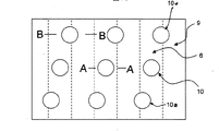
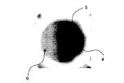
すなわち、半導体デバイスにおいて、第1配線層と第2配線層とは絶縁層中に形成されたビアホールを介して接続されている。尚、このビアホールはエッチングによって形成される。このエッチングに際して、オーバーエッチングが行われると、ビアホール下の第1配線層を構成するCuまでもがエッチングされることになる。その結果、Cuがビアホール内にて飛散し、ビアホール内壁面に付着・堆積し、支障が起きる。この為、オーバーエッチングを出来るだけ少なくすることが求められる。
前記第1の配線パターンを形成した後、該第1の配線パターン上に絶縁層を形成する絶縁層形成工程と、
前記絶縁層形成工程の後、前記第1の配線パターンに適合する前記所定パターンのビアホールを前記絶縁層に形成する適合ビアホール形成工程と、
前記絶縁層形成工程の後、前記第1の配線パターンに一部適合・一部不適合の不適合ビアホールを形成する不適合ビアホール形成工程と、
前記不適合ビアホール形成工程で形成されたビアホールを調べることによって前記適合ビアホール形成工程を制御する制御工程
とを具備することを特徴とするビアホール形成方法によって解決される。
前記第1の配線パターンを形成した後、該第1の配線パターン上に絶縁層を形成する絶縁層形成工程と、
前記絶縁層形成工程の後、前記第1の配線パターンに適合する前記所定パターンのビアホールを前記絶縁層に形成する適合ビアホール形成工程と、
前記絶縁層形成工程の後、ビアホールの一部が第1の配線パターンの領域内に存在し、該ビアホールの残部が第1の配線パターンの領域外に存在する一部適合・一部不適合の不適合ビアホールを形成する不適合ビアホール形成工程と、
前記不適合ビアホール形成工程で形成されたビアホールを調べることによって前記適合ビアホール形成工程を制御する制御工程
とを具備することを特徴とするビアホール形成方法によって解決される。
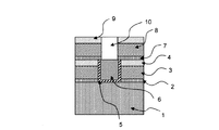
2 配線ストッパ膜
3 配線層間膜
4 配線キャップ膜
5 バリア膜
6 Cu配線膜
7 ビアホールストッパ膜
8 ビアホール層間膜
9 ビアホールキャップ膜
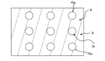
10 ビアホール(適合ビアホール)
10a ビアホール(不適合ビアホール)
代 理 人 宇 高 克 己
Claims (7)
- 第1の配線パターンと第2の配線パターンとを接続する為に用いられる所定パターンのビアホールを形成する為の方法であって、
前記第1の配線パターンを形成した後、該第1の配線パターン上に絶縁層を形成する絶縁層形成工程と、
前記絶縁層形成工程の後、前記第1の配線パターンに適合する前記所定パターンのビアホールを前記絶縁層に形成する適合ビアホール形成工程と、
前記絶縁層形成工程の後、前記第1の配線パターンに一部適合・一部不適合の不適合ビアホールを形成する不適合ビアホール形成工程と、
前記不適合ビアホール形成工程で形成されたビアホールを調べることによって前記適合ビアホール形成工程を制御する制御工程
とを具備することを特徴とするビアホール形成方法。 - 不適合ビアホール形成工程は、
該ビアホールの一部が第1の配線パターンの領域内に存在し、該ビアホールの残部が第1の配線パターンの領域外に存在する一部適合・一部不適合の不適合ビアホールを形成する工程である
ことを特徴とする請求項1のビアホール形成方法。 - 適合ビアホール形成工程と不適合ビアホール形成工程とを同時進行させ、不適合ビアホール形成工程により形成されるビアホールの底面を調べることによって、前記適合ビアホール形成工程を停止することを特徴とする請求項1又は請求項2のビアホール形成方法。
- 適合ビアホール形成工程と不適合ビアホール形成工程とを同時進行させ、不適合ビアホール形成工程により形成されるビアホールの底面に第1の配線パターン部と非第1の配線パターン部とが検出された場合、前記適合ビアホール形成工程を停止することを特徴とする請求項1又は請求項2のビアホール形成方法。
- ビアホール形成がエッチングにより行われることを特徴とする請求項1〜請求項4いずれかのビアホール形成方法。
- 第1の配線パターンの構成材料がCuであることを特徴とする請求項1〜請求項5いずれかのビアホール形成方法。
- 請求項1〜請求項6いずれかのビアホール形成方法が行われることにより得られてなる半導体装置。
Priority Applications (1)
| Application Number | Priority Date | Filing Date | Title |
|---|---|---|---|
| JP2005177306A JP4591927B2 (ja) | 2005-06-17 | 2005-06-17 | ビアホール形成方法 |
Applications Claiming Priority (1)
| Application Number | Priority Date | Filing Date | Title |
|---|---|---|---|
| JP2005177306A JP4591927B2 (ja) | 2005-06-17 | 2005-06-17 | ビアホール形成方法 |
Publications (2)
| Publication Number | Publication Date |
|---|---|
| JP2006351902A true JP2006351902A (ja) | 2006-12-28 |
| JP4591927B2 JP4591927B2 (ja) | 2010-12-01 |
Family
ID=37647415
Family Applications (1)
| Application Number | Title | Priority Date | Filing Date |
|---|---|---|---|
| JP2005177306A Expired - Fee Related JP4591927B2 (ja) | 2005-06-17 | 2005-06-17 | ビアホール形成方法 |
Country Status (1)
| Country | Link |
|---|---|
| JP (1) | JP4591927B2 (ja) |
Cited By (1)
| Publication number | Priority date | Publication date | Assignee | Title |
|---|---|---|---|---|
| WO2024214612A1 (ja) * | 2023-04-12 | 2024-10-17 | 東京エレクトロン株式会社 | 検査用基板、検査方法及び基板処理システム |
Citations (5)
| Publication number | Priority date | Publication date | Assignee | Title |
|---|---|---|---|---|
| JPH0412531A (ja) * | 1990-05-02 | 1992-01-17 | Oki Electric Ind Co Ltd | 半導体装置の製造方法 |
| JPH06223767A (ja) * | 1993-01-29 | 1994-08-12 | Jeol Ltd | 直接写像型反射電子顕微鏡 |
| JPH10256366A (ja) * | 1997-03-07 | 1998-09-25 | Nec Corp | ビアホールの開孔検査パターン構造 |
| JP2003124277A (ja) * | 2001-10-11 | 2003-04-25 | Fujitsu Ltd | 半導体装置の製造方法及び半導体装置 |
| JP2004119449A (ja) * | 2002-09-24 | 2004-04-15 | Matsushita Electric Ind Co Ltd | 半導体装置及びその製造方法 |
-
2005
- 2005-06-17 JP JP2005177306A patent/JP4591927B2/ja not_active Expired - Fee Related
Patent Citations (5)
| Publication number | Priority date | Publication date | Assignee | Title |
|---|---|---|---|---|
| JPH0412531A (ja) * | 1990-05-02 | 1992-01-17 | Oki Electric Ind Co Ltd | 半導体装置の製造方法 |
| JPH06223767A (ja) * | 1993-01-29 | 1994-08-12 | Jeol Ltd | 直接写像型反射電子顕微鏡 |
| JPH10256366A (ja) * | 1997-03-07 | 1998-09-25 | Nec Corp | ビアホールの開孔検査パターン構造 |
| JP2003124277A (ja) * | 2001-10-11 | 2003-04-25 | Fujitsu Ltd | 半導体装置の製造方法及び半導体装置 |
| JP2004119449A (ja) * | 2002-09-24 | 2004-04-15 | Matsushita Electric Ind Co Ltd | 半導体装置及びその製造方法 |
Cited By (1)
| Publication number | Priority date | Publication date | Assignee | Title |
|---|---|---|---|---|
| WO2024214612A1 (ja) * | 2023-04-12 | 2024-10-17 | 東京エレクトロン株式会社 | 検査用基板、検査方法及び基板処理システム |
Also Published As
| Publication number | Publication date |
|---|---|
| JP4591927B2 (ja) | 2010-12-01 |
Similar Documents
| Publication | Publication Date | Title |
|---|---|---|
| US7470616B1 (en) | Damascene wiring fabrication methods incorporating dielectric cap etch process with hard mask retention | |
| US8093074B2 (en) | Analysis method for semiconductor device | |
| US8114688B2 (en) | Method and semiconductor structure for monitoring etch characteristics during fabrication of vias of interconnect structures | |
| US7511349B2 (en) | Contact or via hole structure with enlarged bottom critical dimension | |
| TWI435410B (zh) | 藉由設置假通孔而增加金屬化層之附著力之技術 | |
| US5214283A (en) | Method of determining the cause of open-via failures in an integrated circuit | |
| US6168977B1 (en) | Method of manufacturing a semiconductor device having conductive patterns | |
| JP4591927B2 (ja) | ビアホール形成方法 | |
| JP4848137B2 (ja) | 半導体装置およびその製造方法 | |
| JP2962281B2 (ja) | 半導体装置の検査パターンおよび半導体装置の検査方法 | |
| US20020106885A1 (en) | Method of fabricating a slot dual damascene structure without middle stop layer | |
| KR100996305B1 (ko) | 반도체 소자의 제조 방법 | |
| US20040157464A1 (en) | Manufacturing method of electronic device having wiring connection structure | |
| US20010014528A1 (en) | Method of manufacturing unlanded via plug | |
| US6444573B1 (en) | Method of making a slot via filled dual damascene structure with a middle stop layer | |
| KR100789612B1 (ko) | 금속 배선 형성 방법 | |
| JP2008021862A (ja) | 半導体装置およびその製造方法 | |
| KR20050064668A (ko) | 듀얼 다마신 패턴 형성 방법 | |
| KR100607748B1 (ko) | 반도체소자의 연결배선 제조 방법 | |
| KR101175276B1 (ko) | 반도체소자의 콘택홀 형성 방법 | |
| KR100750803B1 (ko) | 반도체 소자의 금속 배선 형성 방법 | |
| JP2006245504A (ja) | 半導体装置及びその製造方法 | |
| KR20090064647A (ko) | 반도체소자의 비아 단선 테스트 패턴 및 이를 이용한 비아형성방법 | |
| KR20060074241A (ko) | 반도체 소자의 콘택 제조방법 | |
| KR20040009746A (ko) | 반도체 소자의 듀얼 다마신 패턴 형성방법 |
Legal Events
| Date | Code | Title | Description |
|---|---|---|---|
| A621 | Written request for application examination |
Free format text: JAPANESE INTERMEDIATE CODE: A621 Effective date: 20080602 |
|
| A977 | Report on retrieval |
Free format text: JAPANESE INTERMEDIATE CODE: A971007 Effective date: 20100329 |
|
| A131 | Notification of reasons for refusal |
Free format text: JAPANESE INTERMEDIATE CODE: A131 Effective date: 20100407 |
|
| A521 | Request for written amendment filed |
Free format text: JAPANESE INTERMEDIATE CODE: A523 Effective date: 20100601 |
|
| A131 | Notification of reasons for refusal |
Free format text: JAPANESE INTERMEDIATE CODE: A131 Effective date: 20100623 |
|
| A521 | Request for written amendment filed |
Free format text: JAPANESE INTERMEDIATE CODE: A523 Effective date: 20100819 |
|
| TRDD | Decision of grant or rejection written | ||
| A01 | Written decision to grant a patent or to grant a registration (utility model) |
Free format text: JAPANESE INTERMEDIATE CODE: A01 Effective date: 20100908 |
|
| A01 | Written decision to grant a patent or to grant a registration (utility model) |
Free format text: JAPANESE INTERMEDIATE CODE: A01 |
|
| A61 | First payment of annual fees (during grant procedure) |
Free format text: JAPANESE INTERMEDIATE CODE: A61 Effective date: 20100908 |
|
| FPAY | Renewal fee payment (event date is renewal date of database) |
Free format text: PAYMENT UNTIL: 20130924 Year of fee payment: 3 |
|
| R150 | Certificate of patent or registration of utility model |
Ref document number: 4591927 Country of ref document: JP Free format text: JAPANESE INTERMEDIATE CODE: R150 Free format text: JAPANESE INTERMEDIATE CODE: R150 |
|
| FPAY | Renewal fee payment (event date is renewal date of database) |
Free format text: PAYMENT UNTIL: 20130924 Year of fee payment: 3 |
|
| S111 | Request for change of ownership or part of ownership |
Free format text: JAPANESE INTERMEDIATE CODE: R313113 |
|
| FPAY | Renewal fee payment (event date is renewal date of database) |
Free format text: PAYMENT UNTIL: 20130924 Year of fee payment: 3 |
|
| R350 | Written notification of registration of transfer |
Free format text: JAPANESE INTERMEDIATE CODE: R350 |
|
| R250 | Receipt of annual fees |
Free format text: JAPANESE INTERMEDIATE CODE: R250 |
|
| R250 | Receipt of annual fees |
Free format text: JAPANESE INTERMEDIATE CODE: R250 |
|
| R250 | Receipt of annual fees |
Free format text: JAPANESE INTERMEDIATE CODE: R250 |
|
| R250 | Receipt of annual fees |
Free format text: JAPANESE INTERMEDIATE CODE: R250 |
|
| R250 | Receipt of annual fees |
Free format text: JAPANESE INTERMEDIATE CODE: R250 |
|
| R250 | Receipt of annual fees |
Free format text: JAPANESE INTERMEDIATE CODE: R250 |
|
| LAPS | Cancellation because of no payment of annual fees |