JP2006503473A - 信号の振幅を検出するための方法及び装置 - Google Patents
信号の振幅を検出するための方法及び装置 Download PDFInfo
- Publication number
- JP2006503473A JP2006503473A JP2004544548A JP2004544548A JP2006503473A JP 2006503473 A JP2006503473 A JP 2006503473A JP 2004544548 A JP2004544548 A JP 2004544548A JP 2004544548 A JP2004544548 A JP 2004544548A JP 2006503473 A JP2006503473 A JP 2006503473A
- Authority
- JP
- Japan
- Prior art keywords
- signal
- level
- amplitude
- circuit
- shift
- Prior art date
- Legal status (The legal status is an assumption and is not a legal conclusion. Google has not performed a legal analysis and makes no representation as to the accuracy of the status listed.)
- Granted
Links
- 238000000034 method Methods 0.000 title claims abstract description 12
- 239000003990 capacitor Substances 0.000 description 3
- 230000008878 coupling Effects 0.000 description 3
- 238000010168 coupling process Methods 0.000 description 3
- 238000005859 coupling reaction Methods 0.000 description 3
- 239000013642 negative control Substances 0.000 description 2
- 238000007792 addition Methods 0.000 description 1
- 230000002411 adverse Effects 0.000 description 1
- 230000000295 complement effect Effects 0.000 description 1
- 238000010586 diagram Methods 0.000 description 1
- 230000007613 environmental effect Effects 0.000 description 1
- 238000005259 measurement Methods 0.000 description 1
- 238000012986 modification Methods 0.000 description 1
- 230000004048 modification Effects 0.000 description 1
- 230000007704 transition Effects 0.000 description 1
Images

Classifications
-
- H—ELECTRICITY
- H04—ELECTRIC COMMUNICATION TECHNIQUE
- H04L—TRANSMISSION OF DIGITAL INFORMATION, e.g. TELEGRAPHIC COMMUNICATION
- H04L25/00—Baseband systems
- H04L25/02—Details ; arrangements for supplying electrical power along data transmission lines
- H04L25/06—DC level restoring means; Bias distortion correction ; Decision circuits providing symbol by symbol detection
- H04L25/061—DC level restoring means; Bias distortion correction ; Decision circuits providing symbol by symbol detection providing hard decisions only; arrangements for tracking or suppressing unwanted low frequency components, e.g. removal of DC offset
Landscapes
- Engineering & Computer Science (AREA)
- Power Engineering (AREA)
- Computer Networks & Wireless Communication (AREA)
- Signal Processing (AREA)
- Measurement Of Current Or Voltage (AREA)
- Dc Digital Transmission (AREA)
- Manipulation Of Pulses (AREA)
- Amplifiers (AREA)
- Radar Systems Or Details Thereof (AREA)
- Burglar Alarm Systems (AREA)
Abstract
Description
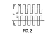
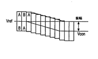
上記信号からあらゆる直流成分を除去して、基準レベルに等しい平均レベルをもつ中間信号を生成するステップと、
中間信号をシフト量の分シフトして、基準レベルに等しい第1の信号レベルをもつシフトされた信号を生成するステップと、
上記シフト量を、信号の振幅の指標(indication,目安)として提供するステップと、
を含む方法を提供することにある。
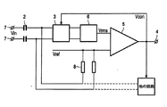
上記信号からあらゆる直流成分を除去して、基準レベルに等しい平均レベルをもつ中間信号を生成するためのデカップリング回路と、
中間信号をシフト量の分シフトして、基準レベルに等しい第1の信号レベルをもつシフトされた信号を生成するためのシフト回路と、
上記シフト量を、上記信号の振幅の指標として提供するための出力端子と、
を有する装置を提供する。
Claims (7)
- 第1の信号レベル及び第2の信号レベルをもつ信号の振幅を決定するための方法であって、
前記信号からあらゆる直流成分を除去して、基準レベルに等しい平均レベルをもつ中間信号を生成するステップと、
前記中間信号をシフト量の分シフトして、前記基準レベルに等しい前記第1の信号レベルをもつシフトされた信号を生成するステップと、
前記シフト量を、前記信号の前記振幅の指標として提供するステップと、
を含む方法。 - 前記シフトされた信号及び前記基準レベルが、前記シフト量を決定する、請求項1に記載の方法。
- 前記シフト量が、継続的に決定される、請求項1又は2に記載の方法。
- 第1の信号レベル及び第2の信号レベルをもつ信号の振幅を決定するための装置であって、
前記信号からあらゆる直流成分を除去して、基準レベルに等しい平均レベルをもつ中間信号を生成するためのデカップリング回路と、
前記中間信号をシフト量の分シフトして、前記基準レベルに等しい前記第1の信号レベルをもつシフトされた信号を生成するためのシフト回路と、
前記シフト量を、前記信号の前記振幅の指標として提供するための出力端子と、
を有する装置。 - 前記シフト回路が、前記シフトされた信号のパワーを示す信号及び前記基準レベルを受け取るように結合される、差動増幅器の出力に結合される、請求項4に記載の装置。
- 信号パワー決定回路が、前記シフト回路と前記差動増幅器との間に結合される、請求項5に記載の装置。
- 前記基準レベルが、電源電圧に等しい、請求項4、5又は6に記載の装置。
Applications Claiming Priority (2)
| Application Number | Priority Date | Filing Date | Title |
|---|---|---|---|
| EP02079305 | 2002-10-17 | ||
| PCT/IB2003/004229 WO2004036859A1 (en) | 2002-10-17 | 2003-09-22 | Method and device for signal amplitude detection |
Publications (2)
| Publication Number | Publication Date |
|---|---|
| JP2006503473A true JP2006503473A (ja) | 2006-01-26 |
| JP4299785B2 JP4299785B2 (ja) | 2009-07-22 |
Family
ID=32103951
Family Applications (1)
| Application Number | Title | Priority Date | Filing Date |
|---|---|---|---|
| JP2004544548A Expired - Fee Related JP4299785B2 (ja) | 2002-10-17 | 2003-09-22 | 信号の振幅を検出するための方法及び装置 |
Country Status (8)
| Country | Link |
|---|---|
| US (1) | US7235985B2 (ja) |
| EP (1) | EP1554850B1 (ja) |
| JP (1) | JP4299785B2 (ja) |
| CN (1) | CN100505716C (ja) |
| AT (1) | ATE347769T1 (ja) |
| AU (1) | AU2003263508A1 (ja) |
| DE (1) | DE60310250T2 (ja) |
| WO (1) | WO2004036859A1 (ja) |
Families Citing this family (1)
| Publication number | Priority date | Publication date | Assignee | Title |
|---|---|---|---|---|
| TWI502443B (zh) * | 2013-10-09 | 2015-10-01 | Ili Technology Corp | 應用於觸控面板基線校正的面板時間延遲檢測電路 |
Family Cites Families (6)
| Publication number | Priority date | Publication date | Assignee | Title |
|---|---|---|---|---|
| US2798198A (en) * | 1952-03-31 | 1957-07-02 | Ca Nat Research Council | Method and apparatus for comparing voltages |
| CA1175919A (en) * | 1980-02-20 | 1984-10-09 | Toshitaka Tsuda | Device for discriminating between two values of a signal with dc offset compensation |
| JP2639326B2 (ja) * | 1993-11-30 | 1997-08-13 | 日本電気株式会社 | 四値fsk受信機 |
| US5907261A (en) * | 1997-09-05 | 1999-05-25 | Ericsson Inc. | Method and apparatus for controlling signal amplitude level |
| FR2772923B1 (fr) * | 1997-12-23 | 2000-03-17 | Sextant Avionique | Circuit electronique de surveillance de tension electrique |
| US6324232B1 (en) * | 1998-01-15 | 2001-11-27 | Pc-Tel, Inc. | Adaptive DC-compensation |
-
2003
- 2003-09-22 JP JP2004544548A patent/JP4299785B2/ja not_active Expired - Fee Related
- 2003-09-22 EP EP03808806A patent/EP1554850B1/en not_active Expired - Lifetime
- 2003-09-22 US US10/531,400 patent/US7235985B2/en not_active Expired - Fee Related
- 2003-09-22 WO PCT/IB2003/004229 patent/WO2004036859A1/en not_active Ceased
- 2003-09-22 DE DE60310250T patent/DE60310250T2/de not_active Expired - Lifetime
- 2003-09-22 AT AT03808806T patent/ATE347769T1/de not_active IP Right Cessation
- 2003-09-22 CN CNB03824277XA patent/CN100505716C/zh not_active Expired - Fee Related
- 2003-09-22 AU AU2003263508A patent/AU2003263508A1/en not_active Abandoned
Also Published As
| Publication number | Publication date |
|---|---|
| CN100505716C (zh) | 2009-06-24 |
| DE60310250D1 (de) | 2007-01-18 |
| US20060012381A1 (en) | 2006-01-19 |
| JP4299785B2 (ja) | 2009-07-22 |
| EP1554850A1 (en) | 2005-07-20 |
| ATE347769T1 (de) | 2006-12-15 |
| WO2004036859A1 (en) | 2004-04-29 |
| CN1689294A (zh) | 2005-10-26 |
| US7235985B2 (en) | 2007-06-26 |
| EP1554850B1 (en) | 2006-12-06 |
| AU2003263508A1 (en) | 2004-05-04 |
| DE60310250T2 (de) | 2007-06-28 |
Similar Documents
| Publication | Publication Date | Title |
|---|---|---|
| EP0774178A1 (en) | Detection circuit with hysteresis proportional to the peak input voltage | |
| JP2924373B2 (ja) | A/d変換回路 | |
| US10901009B2 (en) | Power detector for radiofrequency power amplifier circuits | |
| JP4299785B2 (ja) | 信号の振幅を検出するための方法及び装置 | |
| JP2561023B2 (ja) | 高周波信号レベル検出回路および高周波信号レベル検出方法 | |
| JPS59231456A (ja) | レベル検出装置 | |
| JP2005535196A (ja) | バイナリ信号におけるスライスレベルを設定するための方法及び装置 | |
| JP2004071864A (ja) | 半導体集積回路の温度検出装置 | |
| JP2000155139A (ja) | 電流検出装置 | |
| KR102013999B1 (ko) | 포화 검출기 | |
| KR0183939B1 (ko) | 제로 크로스 감지회로 | |
| KR940006892B1 (ko) | 레코딩 장치의 신호검출회로 | |
| JPH08125697A (ja) | Ask変調における復調回路 | |
| JP3285191B2 (ja) | 検相回路 | |
| JP2007240286A (ja) | 計測方法および計測装置 | |
| KR100187937B1 (ko) | 교차 코일형 아날로그 지시계기용 상반전압 생성회로 | |
| RU1835085C (ru) | Источник опорного напр жени | |
| JPS62169515A (ja) | 半導体集積回路 | |
| JPS6333750B2 (ja) | ||
| JP2006025260A (ja) | 増幅回路、及び試験装置 | |
| JPH04370770A (ja) | ピーク値検出回路 | |
| KR19990018197A (ko) | 오프셋 전압을 이용한 기준전압 발생회로 | |
| KR19980052130A (ko) | 포텐셔 미터(Potentiometer) | |
| JPS59203963A (ja) | レベル判定回路 | |
| JP2003273645A (ja) | 電圧/周波数変換回路およびその制御方法 |
Legal Events
| Date | Code | Title | Description |
|---|---|---|---|
| A621 | Written request for application examination |
Free format text: JAPANESE INTERMEDIATE CODE: A621 Effective date: 20060922 |
|
| RD03 | Notification of appointment of power of attorney |
Free format text: JAPANESE INTERMEDIATE CODE: A7423 Effective date: 20070326 |
|
| A711 | Notification of change in applicant |
Free format text: JAPANESE INTERMEDIATE CODE: A711 Effective date: 20080424 |
|
| A977 | Report on retrieval |
Free format text: JAPANESE INTERMEDIATE CODE: A971007 Effective date: 20090410 |
|
| TRDD | Decision of grant or rejection written | ||
| A01 | Written decision to grant a patent or to grant a registration (utility model) |
Free format text: JAPANESE INTERMEDIATE CODE: A01 Effective date: 20090414 |
|
| A01 | Written decision to grant a patent or to grant a registration (utility model) |
Free format text: JAPANESE INTERMEDIATE CODE: A01 |
|
| A61 | First payment of annual fees (during grant procedure) |
Free format text: JAPANESE INTERMEDIATE CODE: A61 Effective date: 20090417 |
|
| R150 | Certificate of patent or registration of utility model |
Free format text: JAPANESE INTERMEDIATE CODE: R150 |
|
| FPAY | Renewal fee payment (event date is renewal date of database) |
Free format text: PAYMENT UNTIL: 20120424 Year of fee payment: 3 |
|
| LAPS | Cancellation because of no payment of annual fees |