JP2006524905A - メモリ回路構造およびその製造方法 - Google Patents
メモリ回路構造およびその製造方法 Download PDFInfo
- Publication number
- JP2006524905A JP2006524905A JP2006500119A JP2006500119A JP2006524905A JP 2006524905 A JP2006524905 A JP 2006524905A JP 2006500119 A JP2006500119 A JP 2006500119A JP 2006500119 A JP2006500119 A JP 2006500119A JP 2006524905 A JP2006524905 A JP 2006524905A
- Authority
- JP
- Japan
- Prior art keywords
- memory cell
- cell array
- memory
- substrate
- circuit
- Prior art date
- Legal status (The legal status is an assumption and is not a legal conclusion. Google has not performed a legal analysis and makes no representation as to the accuracy of the status listed.)
- Pending
Links
Images


Classifications
-
- G—PHYSICS
- G11—INFORMATION STORAGE
- G11C—STATIC STORES
- G11C5/00—Details of stores covered by group G11C11/00
- G11C5/02—Disposition of storage elements, e.g. in the form of a matrix array
- G11C5/025—Geometric lay-out considerations of storage- and peripheral-blocks in a semiconductor storage device
-
- H—ELECTRICITY
- H10—SEMICONDUCTOR DEVICES; ELECTRIC SOLID-STATE DEVICES NOT OTHERWISE PROVIDED FOR
- H10W—GENERIC PACKAGES, INTERCONNECTIONS, CONNECTORS OR OTHER CONSTRUCTIONAL DETAILS OF DEVICES COVERED BY CLASS H10
- H10W90/00—Package configurations
Landscapes
- Engineering & Computer Science (AREA)
- Microelectronics & Electronic Packaging (AREA)
- Semiconductor Memories (AREA)
- Static Random-Access Memory (AREA)
- Semiconductor Integrated Circuits (AREA)
- Non-Volatile Memory (AREA)
Abstract
Description
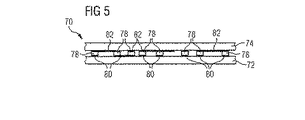
・導電性接着接続部
・導電性溶接接続部
・導電性ボンディング接続部
・例えば、EP 0 610 709 A1に記載の、溶媒を含んだ混合物を硬化させることにより製造された接続部、または
・メモリセル用基板、または論理回路用基板を貫通する金属化接続部(参照:DE 199 04 751 C1)
本実施形態では、基板間の接続部の数は、ワード線の数および/またはビット線の数に応じて決まる。したがって、例えば、接続部の数は、1000以上、2000以上、または3000以上であり、メモリセルアレイの記憶容量に応じて決まる。
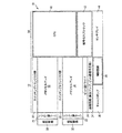
・メモリセルアレイ16、18、
・ワード線ドライバトランジスタ20、22、
・ビット線ドライバトランジスタ24、
・ワード線復号回路34、
・チャージポンプ36、および
・センサアレイ44の、センサおよび変換器を搭載している。
・制御回路38、
・プロセッサ40、および
・暗号化コプロセッサ42を搭載している。
・メモリセルアレイ16、18、
・ワード線ドライバトランジスタ20、22、
・ビット線ドライバトランジスタ24、
・チャージポンプ36、および
・センサアレイ44のセンサおよび変換器が形成されている。
・ワード線復号回路30、32、
・論理回路34、
・制御回路38、
・プロセッサ40、および
・暗号化コプロセッサ42が形成されている。
・ONO積層(酸化物/窒化物/酸化物)に基づいて、特にデータ保存時間に関して、誘電定数の高い誘電体を実現するという課題、
・これらの誘電体用の異方性エッチング方法、特に、異方性イオンエッチング方法、を使用できるようにするという課題、および
・側壁酸化を実現する、例えば、誘電体が結晶化するという課題である。
・データ保存時間に影響を与える転位による、シリコンの過度の使用における課題。
Claims (9)
- 複数のメモリセルを有する集積メモリセルアレイ(16)が搭載されてなるメモリセルアレイ用基板(52)と、
メモリセルへのアクセスを制御し、メモリ回路構造の基本的機能を実現する少なくとも1つの集積論理回路(30、38)が搭載されてなる論理回路用基板(54)とを備え、
上記論理回路用基板(54)は、上記メモリセルアレイ用基板(52)とは異なる基板であることを特徴とするメモリ回路構造(10)。 - 上記メモリセルアレイ用基板(52)の何れの表面も、該メモリセルアレイ用基板(52)のみを囲むように配置されており、上記論理回路用基板(54)を囲むようには配置されておらず、かつ/または上記メモリセルは、揮発性メモリセル、または不揮発性メモリセル、特にフラッシュメモリセルであることを特徴とする、請求項1に記載のメモリ回路構造(10)。
- 上記論理回路用基板(54)は、さらに、メモリセルアレイ(16)のメモリセルの内容の読み出し順序および/または書き込み順序および/または消去順序を制御するための制御回路(38)、および/または上記メモリセルの記憶状態を検出可能な検出アンプ回路(34)を搭載してなることを特徴とする請求項1または2に記載のメモリ回路構造(10)。
- 上記論理回路用基板(54)は、少なくとも1つの復号回路(30、34)を含んでおり、上記復号回路は、アドレスデータに基づいて、上記メモリセルアレイ(16)の複数のメモリセルに接続されている選択線、特に、上記メモリセルアレイ(16)のメモリセルの中の所定の行に配されたメモリセルに接続されたワード線および/またはメモリセルアレイ(16)のメモリセルのうちの所定の列に配置されたメモリセルに接続されたビット線を選択し、かつ/または各選択線に対応して設けられた上記セルアレイ用基板(52)と上記論理回路基板(54)との間の導電性接続部により選択されることを特徴とする、請求項1ないし3のいずれか1項に記載のメモリ回路構造(10)。
- 上記論理回路用基板(54)は、少なくとも1つのプロセッサ(40、42)の回路構造を搭載しており、上記プロセッサ(40、42)は、プログラム命令の処理に適しており、特に、上記メモリセルアレイに格納されたプログラム命令の処理に適しており、特に、動作中に暗号化プログラムのプログラム命令、特にメモリセルアレイ(16)に格納されたプログラム命令、を実行する暗号化プロセッサ(42)であり、かつ/または
上記メモリセルアレイ用基板(52)は、少なくとも1つのアナログ回路、特に、電圧検出ユニットおよび/または電流検出ユニット(44)および/または少なくとも1つのアナログデジタル変換器ユニットおよび/またはデジタル/アナログ変換器ユニットが搭載されてなることを特徴とする、請求項1ないし4のいずれか1項に記載のメモリ回路構造(10)。 - 上記メモリセルアレイ用基板(52)の主領域と、論理回路用基板(54)の主領域とは、互いに平行に、好ましくは主領域の法線方向に重なり合って配された2つの平面上に設けられており、または
上記メモリセルアレイ用基板の主領域は、上記論理回路用基板の主領域を横断するように設けられていることを特徴とする、請求項1ないし5のいずれか1項に記載のメモリ回路構造(10)。 - 回路構造、特に、請求項1ないし6のいずれか1項に記載の集積回路構造(10)の製造方法であって、
メモリセルアレイ用基板(52)に集積メモリセルアレイ(16)を形成する第1工程と、
上記集積メモリセルアレイ用基板(52)と離れた位置に配置される論理回路用基板(54)に、上記メモリセルアレイ(16)の基本的機能を実現する集積論理回路を形成する第1工程とは異なる第2工程と、
メモリ回路構造(10、50)を形成するために、上記集積メモリセルアレイ(52)と上記集積論理用回路(54)とを配置する工程とを含み、上記各工程の実施順序は限定されないことを特徴とする集積回路構造(10)の製造方法。 - 上記第1工程は、
さらに、1μmまたは2μmよりも深いトレンチを形成する工程と、
6ボルト以上の電圧で、特に、端部において上記6ボルト以上の電圧に適したドーピング勾配を有する少なくとも1つのn型ウェルまたはn型層および/または少なくとも1つのp型ウェルまたはp型層を形成する工程と、
トンネル酸化物を形成する工程と、
2つの酸化物層の間に絶縁性電極を形成する工程と、
上記絶縁性電極上の選択された電極を除去する工程と、
50nmよりも厚い酸化物領域を形成する工程と、
6ボルトよりも高い電圧でチャネル接続領域を形成する工程とのうち、少なくとも1つの上記第2工程には含まれない工程を含んでおり、かつ/または
上記第2工程は、
さらに、深さが1μm、または0.5μmよりも浅い、浅いトレンチを形成する工程と、
5ボルトまたは2.5ボルトよりも低い電圧で、少なくとも1つのn型ウェルまたはn型層および/または少なくとも1つのp型ウェルまたはp型層を形成する工程と、
5ボルトまたは2.5ボルトよりも低い電圧で、チャネル接続領域を形成する工程と、
第1工程よりも多くの少なくとも1つの金属化層を形成する工程とのうち、少なくとも1つの工程を含んでおり、上記少なくとも1つの工程は、上記第1工程には含まれていないことを特徴とする、請求項7に記載の製造方法。 - 高速チップ実装技術または3D集積方法を用いて、メモリセルアレイ用基板(52)と論理回路用基板(54)とを配置することを特徴とする、請求項7または8に記載の製造方法。
Applications Claiming Priority (2)
| Application Number | Priority Date | Filing Date | Title |
|---|---|---|---|
| DE10319271A DE10319271A1 (de) | 2003-04-29 | 2003-04-29 | Speicher-Schaltungsanordnung und Verfahren zur Herstellung |
| PCT/EP2004/050322 WO2004097838A2 (de) | 2003-04-29 | 2004-03-17 | Speicher-schaltungsanordnung und verfahren zur herstellung |
Publications (1)
| Publication Number | Publication Date |
|---|---|
| JP2006524905A true JP2006524905A (ja) | 2006-11-02 |
Family
ID=33393972
Family Applications (1)
| Application Number | Title | Priority Date | Filing Date |
|---|---|---|---|
| JP2006500119A Pending JP2006524905A (ja) | 2003-04-29 | 2004-03-17 | メモリ回路構造およびその製造方法 |
Country Status (6)
| Country | Link |
|---|---|
| US (5) | US7460385B2 (ja) |
| EP (1) | EP1618570B1 (ja) |
| JP (1) | JP2006524905A (ja) |
| CN (1) | CN100538867C (ja) |
| DE (2) | DE10319271A1 (ja) |
| WO (1) | WO2004097838A2 (ja) |
Cited By (3)
| Publication number | Priority date | Publication date | Assignee | Title |
|---|---|---|---|---|
| WO2013128806A1 (ja) * | 2012-02-28 | 2013-09-06 | パナソニック株式会社 | 昇圧回路 |
| JP2015188071A (ja) * | 2014-03-14 | 2015-10-29 | 株式会社半導体エネルギー研究所 | 半導体装置 |
| US10897812B2 (en) | 2018-12-25 | 2021-01-19 | AT&S (Chongqing) Company Limited | Component carrier having a component shielding and method of manufacturing the same |
Families Citing this family (182)
| Publication number | Priority date | Publication date | Assignee | Title |
|---|---|---|---|---|
| US7884349B2 (en) * | 2002-08-02 | 2011-02-08 | Unity Semiconductor Corporation | Selection device for re-writable memory |
| US7186569B2 (en) * | 2002-08-02 | 2007-03-06 | Unity Semiconductor Corporation | Conductive memory stack with sidewall |
| DE10319271A1 (de) * | 2003-04-29 | 2004-11-25 | Infineon Technologies Ag | Speicher-Schaltungsanordnung und Verfahren zur Herstellung |
| US7538338B2 (en) * | 2004-09-03 | 2009-05-26 | Unity Semiconductor Corporation | Memory using variable tunnel barrier widths |
| US20060171200A1 (en) | 2004-02-06 | 2006-08-03 | Unity Semiconductor Corporation | Memory using mixed valence conductive oxides |
| US7082052B2 (en) | 2004-02-06 | 2006-07-25 | Unity Semiconductor Corporation | Multi-resistive state element with reactive metal |
| US20130082232A1 (en) | 2011-09-30 | 2013-04-04 | Unity Semiconductor Corporation | Multi Layered Conductive Metal Oxide Structures And Methods For Facilitating Enhanced Performance Characteristics Of Two Terminal Memory Cells |
| US9058300B2 (en) * | 2005-03-30 | 2015-06-16 | Unity Semiconductor Corporation | Integrated circuits and methods to control access to multiple layers of memory |
| US8003511B2 (en) * | 2008-12-19 | 2011-08-23 | Unity Semiconductor Corporation | Memory cell formation using ion implant isolated conductive metal oxide |
| US8031509B2 (en) * | 2008-12-19 | 2011-10-04 | Unity Semiconductor Corporation | Conductive metal oxide structures in non-volatile re-writable memory devices |
| US7897951B2 (en) * | 2007-07-26 | 2011-03-01 | Unity Semiconductor Corporation | Continuous plane of thin-film materials for a two-terminal cross-point memory |
| US8314024B2 (en) | 2008-12-19 | 2012-11-20 | Unity Semiconductor Corporation | Device fabrication |
| US7619945B2 (en) * | 2006-08-18 | 2009-11-17 | Unity Semiconductor Corporation | Memory power management |
| US7539811B2 (en) * | 2006-10-05 | 2009-05-26 | Unity Semiconductor Corporation | Scaleable memory systems using third dimension memory |
| US7742323B2 (en) * | 2007-07-26 | 2010-06-22 | Unity Semiconductor Corporation | Continuous plane of thin-film materials for a two-terminal cross-point memory |
| US7995371B2 (en) * | 2007-07-26 | 2011-08-09 | Unity Semiconductor Corporation | Threshold device for a memory array |
| US7813210B2 (en) * | 2007-08-16 | 2010-10-12 | Unity Semiconductor Corporation | Multiple-type memory |
| US7996600B2 (en) | 2007-08-30 | 2011-08-09 | Unity Semiconductor Corporation | Memory emulation in an electronic organizer |
| US8164656B2 (en) * | 2007-08-31 | 2012-04-24 | Unity Semiconductor Corporation | Memory emulation in an image capture device |
| US7688665B2 (en) * | 2007-09-25 | 2010-03-30 | Qimonda North America Corp. | Structure to share internally generated voltages between chips in MCP |
| US8165621B2 (en) * | 2007-10-10 | 2012-04-24 | Unity Semiconductor Corporation | Memory emulation in a cellular telephone |
| US7593284B2 (en) * | 2007-10-17 | 2009-09-22 | Unity Semiconductor Corporation | Memory emulation using resistivity-sensitive memory |
| US7796451B2 (en) * | 2007-12-10 | 2010-09-14 | Unity Semiconductor Corporation | Integrated circuits and methods to compensate for defective memory in multiple layers of memory |
| US7822913B2 (en) * | 2007-12-20 | 2010-10-26 | Unity Semiconductor Corporation | Emulation of a NAND memory system |
| US7751221B2 (en) * | 2007-12-21 | 2010-07-06 | Unity Semiconductor Corporation | Media player with non-volatile memory |
| US7877541B2 (en) * | 2007-12-22 | 2011-01-25 | Unity Semiconductor Corporation | Method and system for accessing non-volatile memory |
| US20090172350A1 (en) * | 2007-12-28 | 2009-07-02 | Unity Semiconductor Corporation | Non-volatile processor register |
| US7990762B2 (en) * | 2008-02-06 | 2011-08-02 | Unity Semiconductor Corporation | Integrated circuits to control access to multiple layers of memory |
| US8208284B2 (en) * | 2008-03-07 | 2012-06-26 | Unity Semiconductor Corporation | Data retention structure for non-volatile memory |
| US8027215B2 (en) | 2008-12-19 | 2011-09-27 | Unity Semiconductor Corporation | Array operation using a schottky diode as a non-ohmic isolation device |
| US8222090B2 (en) * | 2009-08-04 | 2012-07-17 | Fairchild Semiconductor Corporation | Modular die and mask for semiconductor processing |
| KR101094917B1 (ko) * | 2009-11-30 | 2011-12-15 | 주식회사 하이닉스반도체 | 전원 회로 및 이를 이용한 반도체 메모리 회로 |
| US8045364B2 (en) * | 2009-12-18 | 2011-10-25 | Unity Semiconductor Corporation | Non-volatile memory device ion barrier |
| US7832090B1 (en) | 2010-02-25 | 2010-11-16 | Unity Semiconductor Corporation | Method of making a planar electrode |
| US8728947B2 (en) * | 2012-06-08 | 2014-05-20 | Tel Epion Inc. | Gas cluster ion beam process for opening conformal layer in a high aspect ratio contact via |
| US9158667B2 (en) | 2013-03-04 | 2015-10-13 | Micron Technology, Inc. | Apparatuses and methods for performing logical operations using sensing circuitry |
| US8964496B2 (en) | 2013-07-26 | 2015-02-24 | Micron Technology, Inc. | Apparatuses and methods for performing compare operations using sensing circuitry |
| US8971124B1 (en) | 2013-08-08 | 2015-03-03 | Micron Technology, Inc. | Apparatuses and methods for performing logical operations using sensing circuitry |
| US9153305B2 (en) | 2013-08-30 | 2015-10-06 | Micron Technology, Inc. | Independently addressable memory array address spaces |
| US9019785B2 (en) | 2013-09-19 | 2015-04-28 | Micron Technology, Inc. | Data shifting via a number of isolation devices |
| US9449675B2 (en) | 2013-10-31 | 2016-09-20 | Micron Technology, Inc. | Apparatuses and methods for identifying an extremum value stored in an array of memory cells |
| US9430191B2 (en) | 2013-11-08 | 2016-08-30 | Micron Technology, Inc. | Division operations for memory |
| CN103794238B (zh) * | 2014-03-07 | 2017-01-04 | 中国科学院微电子研究所 | 闪存式存储器电路及其布局方法 |
| US9934856B2 (en) | 2014-03-31 | 2018-04-03 | Micron Technology, Inc. | Apparatuses and methods for comparing data patterns in memory |
| US9496023B2 (en) | 2014-06-05 | 2016-11-15 | Micron Technology, Inc. | Comparison operations on logical representations of values in memory |
| US10074407B2 (en) | 2014-06-05 | 2018-09-11 | Micron Technology, Inc. | Apparatuses and methods for performing invert operations using sensing circuitry |
| US9910787B2 (en) | 2014-06-05 | 2018-03-06 | Micron Technology, Inc. | Virtual address table |
| US9711207B2 (en) | 2014-06-05 | 2017-07-18 | Micron Technology, Inc. | Performing logical operations using sensing circuitry |
| US9786335B2 (en) | 2014-06-05 | 2017-10-10 | Micron Technology, Inc. | Apparatuses and methods for performing logical operations using sensing circuitry |
| US9449674B2 (en) | 2014-06-05 | 2016-09-20 | Micron Technology, Inc. | Performing logical operations using sensing circuitry |
| US9830999B2 (en) | 2014-06-05 | 2017-11-28 | Micron Technology, Inc. | Comparison operations in memory |
| US9455020B2 (en) | 2014-06-05 | 2016-09-27 | Micron Technology, Inc. | Apparatuses and methods for performing an exclusive or operation using sensing circuitry |
| US9711206B2 (en) | 2014-06-05 | 2017-07-18 | Micron Technology, Inc. | Performing logical operations using sensing circuitry |
| US9704540B2 (en) | 2014-06-05 | 2017-07-11 | Micron Technology, Inc. | Apparatuses and methods for parity determination using sensing circuitry |
| US9779019B2 (en) | 2014-06-05 | 2017-10-03 | Micron Technology, Inc. | Data storage layout |
| US9904515B2 (en) | 2014-09-03 | 2018-02-27 | Micron Technology, Inc. | Multiplication operations in memory |
| US9589602B2 (en) | 2014-09-03 | 2017-03-07 | Micron Technology, Inc. | Comparison operations in memory |
| US9740607B2 (en) | 2014-09-03 | 2017-08-22 | Micron Technology, Inc. | Swap operations in memory |
| US10068652B2 (en) | 2014-09-03 | 2018-09-04 | Micron Technology, Inc. | Apparatuses and methods for determining population count |
| US9747961B2 (en) | 2014-09-03 | 2017-08-29 | Micron Technology, Inc. | Division operations in memory |
| US9898252B2 (en) | 2014-09-03 | 2018-02-20 | Micron Technology, Inc. | Multiplication operations in memory |
| US9847110B2 (en) | 2014-09-03 | 2017-12-19 | Micron Technology, Inc. | Apparatuses and methods for storing a data value in multiple columns of an array corresponding to digits of a vector |
| US9836218B2 (en) | 2014-10-03 | 2017-12-05 | Micron Technology, Inc. | Computing reduction and prefix sum operations in memory |
| US9940026B2 (en) | 2014-10-03 | 2018-04-10 | Micron Technology, Inc. | Multidimensional contiguous memory allocation |
| US10163467B2 (en) | 2014-10-16 | 2018-12-25 | Micron Technology, Inc. | Multiple endianness compatibility |
| US10147480B2 (en) | 2014-10-24 | 2018-12-04 | Micron Technology, Inc. | Sort operation in memory |
| US9779784B2 (en) | 2014-10-29 | 2017-10-03 | Micron Technology, Inc. | Apparatuses and methods for performing logical operations using sensing circuitry |
| US9747960B2 (en) | 2014-12-01 | 2017-08-29 | Micron Technology, Inc. | Apparatuses and methods for converting a mask to an index |
| US10073635B2 (en) | 2014-12-01 | 2018-09-11 | Micron Technology, Inc. | Multiple endianness compatibility |
| US10032493B2 (en) | 2015-01-07 | 2018-07-24 | Micron Technology, Inc. | Longest element length determination in memory |
| US10061590B2 (en) | 2015-01-07 | 2018-08-28 | Micron Technology, Inc. | Generating and executing a control flow |
| US9583163B2 (en) | 2015-02-03 | 2017-02-28 | Micron Technology, Inc. | Loop structure for operations in memory |
| WO2016126474A1 (en) | 2015-02-06 | 2016-08-11 | Micron Technology, Inc. | Apparatuses and methods for parallel writing to multiple memory device locations |
| WO2016126478A1 (en) | 2015-02-06 | 2016-08-11 | Micron Technology, Inc. | Apparatuses and methods for memory device as a store for program instructions |
| WO2016126472A1 (en) | 2015-02-06 | 2016-08-11 | Micron Technology, Inc. | Apparatuses and methods for scatter and gather |
| CN107408408B (zh) | 2015-03-10 | 2021-03-05 | 美光科技公司 | 用于移位决定的装置及方法 |
| US9898253B2 (en) | 2015-03-11 | 2018-02-20 | Micron Technology, Inc. | Division operations on variable length elements in memory |
| US9741399B2 (en) | 2015-03-11 | 2017-08-22 | Micron Technology, Inc. | Data shift by elements of a vector in memory |
| WO2016144726A1 (en) | 2015-03-12 | 2016-09-15 | Micron Technology, Inc. | Apparatuses and methods for data movement |
| US10146537B2 (en) | 2015-03-13 | 2018-12-04 | Micron Technology, Inc. | Vector population count determination in memory |
| US10049054B2 (en) | 2015-04-01 | 2018-08-14 | Micron Technology, Inc. | Virtual register file |
| US10140104B2 (en) | 2015-04-14 | 2018-11-27 | Micron Technology, Inc. | Target architecture determination |
| US9959923B2 (en) | 2015-04-16 | 2018-05-01 | Micron Technology, Inc. | Apparatuses and methods to reverse data stored in memory |
| US10073786B2 (en) | 2015-05-28 | 2018-09-11 | Micron Technology, Inc. | Apparatuses and methods for compute enabled cache |
| US9704541B2 (en) | 2015-06-12 | 2017-07-11 | Micron Technology, Inc. | Simulating access lines |
| US9921777B2 (en) | 2015-06-22 | 2018-03-20 | Micron Technology, Inc. | Apparatuses and methods for data transfer from sensing circuitry to a controller |
| US9996479B2 (en) | 2015-08-17 | 2018-06-12 | Micron Technology, Inc. | Encryption of executables in computational memory |
| US9905276B2 (en) | 2015-12-21 | 2018-02-27 | Micron Technology, Inc. | Control of sensing components in association with performing operations |
| US9952925B2 (en) | 2016-01-06 | 2018-04-24 | Micron Technology, Inc. | Error code calculation on sensing circuitry |
| US10048888B2 (en) | 2016-02-10 | 2018-08-14 | Micron Technology, Inc. | Apparatuses and methods for partitioned parallel data movement |
| US9892767B2 (en) | 2016-02-12 | 2018-02-13 | Micron Technology, Inc. | Data gathering in memory |
| US9971541B2 (en) | 2016-02-17 | 2018-05-15 | Micron Technology, Inc. | Apparatuses and methods for data movement |
| US10956439B2 (en) | 2016-02-19 | 2021-03-23 | Micron Technology, Inc. | Data transfer with a bit vector operation device |
| US9899070B2 (en) | 2016-02-19 | 2018-02-20 | Micron Technology, Inc. | Modified decode for corner turn |
| US9697876B1 (en) | 2016-03-01 | 2017-07-04 | Micron Technology, Inc. | Vertical bit vector shift in memory |
| US10262721B2 (en) | 2016-03-10 | 2019-04-16 | Micron Technology, Inc. | Apparatuses and methods for cache invalidate |
| US9997232B2 (en) | 2016-03-10 | 2018-06-12 | Micron Technology, Inc. | Processing in memory (PIM) capable memory device having sensing circuitry performing logic operations |
| US10379772B2 (en) | 2016-03-16 | 2019-08-13 | Micron Technology, Inc. | Apparatuses and methods for operations using compressed and decompressed data |
| US9910637B2 (en) | 2016-03-17 | 2018-03-06 | Micron Technology, Inc. | Signed division in memory |
| US11074988B2 (en) | 2016-03-22 | 2021-07-27 | Micron Technology, Inc. | Apparatus and methods for debugging on a host and memory device |
| US10120740B2 (en) | 2016-03-22 | 2018-11-06 | Micron Technology, Inc. | Apparatus and methods for debugging on a memory device |
| US10388393B2 (en) | 2016-03-22 | 2019-08-20 | Micron Technology, Inc. | Apparatus and methods for debugging on a host and memory device |
| US10977033B2 (en) | 2016-03-25 | 2021-04-13 | Micron Technology, Inc. | Mask patterns generated in memory from seed vectors |
| US10474581B2 (en) | 2016-03-25 | 2019-11-12 | Micron Technology, Inc. | Apparatuses and methods for cache operations |
| US10430244B2 (en) | 2016-03-28 | 2019-10-01 | Micron Technology, Inc. | Apparatuses and methods to determine timing of operations |
| US10074416B2 (en) | 2016-03-28 | 2018-09-11 | Micron Technology, Inc. | Apparatuses and methods for data movement |
| US10453502B2 (en) | 2016-04-04 | 2019-10-22 | Micron Technology, Inc. | Memory bank power coordination including concurrently performing a memory operation in a selected number of memory regions |
| US10607665B2 (en) | 2016-04-07 | 2020-03-31 | Micron Technology, Inc. | Span mask generation |
| US9818459B2 (en) | 2016-04-19 | 2017-11-14 | Micron Technology, Inc. | Invert operations using sensing circuitry |
| US10153008B2 (en) | 2016-04-20 | 2018-12-11 | Micron Technology, Inc. | Apparatuses and methods for performing corner turn operations using sensing circuitry |
| US9659605B1 (en) | 2016-04-20 | 2017-05-23 | Micron Technology, Inc. | Apparatuses and methods for performing corner turn operations using sensing circuitry |
| US10042608B2 (en) | 2016-05-11 | 2018-08-07 | Micron Technology, Inc. | Signed division in memory |
| US9659610B1 (en) | 2016-05-18 | 2017-05-23 | Micron Technology, Inc. | Apparatuses and methods for shifting data |
| US10049707B2 (en) | 2016-06-03 | 2018-08-14 | Micron Technology, Inc. | Shifting data |
| US10387046B2 (en) | 2016-06-22 | 2019-08-20 | Micron Technology, Inc. | Bank to bank data transfer |
| US10037785B2 (en) | 2016-07-08 | 2018-07-31 | Micron Technology, Inc. | Scan chain operation in sensing circuitry |
| US10388360B2 (en) | 2016-07-19 | 2019-08-20 | Micron Technology, Inc. | Utilization of data stored in an edge section of an array |
| US10387299B2 (en) | 2016-07-20 | 2019-08-20 | Micron Technology, Inc. | Apparatuses and methods for transferring data |
| US10733089B2 (en) | 2016-07-20 | 2020-08-04 | Micron Technology, Inc. | Apparatuses and methods for write address tracking |
| US9767864B1 (en) | 2016-07-21 | 2017-09-19 | Micron Technology, Inc. | Apparatuses and methods for storing a data value in a sensing circuitry element |
| US9972367B2 (en) | 2016-07-21 | 2018-05-15 | Micron Technology, Inc. | Shifting data in sensing circuitry |
| US10303632B2 (en) | 2016-07-26 | 2019-05-28 | Micron Technology, Inc. | Accessing status information |
| US10468087B2 (en) | 2016-07-28 | 2019-11-05 | Micron Technology, Inc. | Apparatuses and methods for operations in a self-refresh state |
| US9990181B2 (en) | 2016-08-03 | 2018-06-05 | Micron Technology, Inc. | Apparatuses and methods for random number generation |
| US11029951B2 (en) | 2016-08-15 | 2021-06-08 | Micron Technology, Inc. | Smallest or largest value element determination |
| US10606587B2 (en) | 2016-08-24 | 2020-03-31 | Micron Technology, Inc. | Apparatus and methods related to microcode instructions indicating instruction types |
| US10466928B2 (en) | 2016-09-15 | 2019-11-05 | Micron Technology, Inc. | Updating a register in memory |
| US10387058B2 (en) | 2016-09-29 | 2019-08-20 | Micron Technology, Inc. | Apparatuses and methods to change data category values |
| US10014034B2 (en) | 2016-10-06 | 2018-07-03 | Micron Technology, Inc. | Shifting data in sensing circuitry |
| US10529409B2 (en) | 2016-10-13 | 2020-01-07 | Micron Technology, Inc. | Apparatuses and methods to perform logical operations using sensing circuitry |
| US9805772B1 (en) | 2016-10-20 | 2017-10-31 | Micron Technology, Inc. | Apparatuses and methods to selectively perform logical operations |
| CN207637499U (zh) | 2016-11-08 | 2018-07-20 | 美光科技公司 | 用于形成在存储器单元阵列上方的计算组件的设备 |
| US10423353B2 (en) | 2016-11-11 | 2019-09-24 | Micron Technology, Inc. | Apparatuses and methods for memory alignment |
| US9761300B1 (en) | 2016-11-22 | 2017-09-12 | Micron Technology, Inc. | Data shift apparatuses and methods |
| CN108428464B (zh) * | 2017-02-13 | 2021-02-26 | 群联电子股份有限公司 | 解码方法、存储器储存装置及存储器控制电路单元 |
| US9792958B1 (en) * | 2017-02-16 | 2017-10-17 | Micron Technology, Inc. | Active boundary quilt architecture memory |
| US10402340B2 (en) | 2017-02-21 | 2019-09-03 | Micron Technology, Inc. | Memory array page table walk |
| US10403352B2 (en) | 2017-02-22 | 2019-09-03 | Micron Technology, Inc. | Apparatuses and methods for compute in data path |
| US10268389B2 (en) | 2017-02-22 | 2019-04-23 | Micron Technology, Inc. | Apparatuses and methods for in-memory operations |
| US10838899B2 (en) | 2017-03-21 | 2020-11-17 | Micron Technology, Inc. | Apparatuses and methods for in-memory data switching networks |
| US10185674B2 (en) | 2017-03-22 | 2019-01-22 | Micron Technology, Inc. | Apparatus and methods for in data path compute operations |
| US11222260B2 (en) | 2017-03-22 | 2022-01-11 | Micron Technology, Inc. | Apparatuses and methods for operating neural networks |
| US10049721B1 (en) | 2017-03-27 | 2018-08-14 | Micron Technology, Inc. | Apparatuses and methods for in-memory operations |
| US10043570B1 (en) | 2017-04-17 | 2018-08-07 | Micron Technology, Inc. | Signed element compare in memory |
| US10147467B2 (en) | 2017-04-17 | 2018-12-04 | Micron Technology, Inc. | Element value comparison in memory |
| US9997212B1 (en) | 2017-04-24 | 2018-06-12 | Micron Technology, Inc. | Accessing data in memory |
| US10942843B2 (en) | 2017-04-25 | 2021-03-09 | Micron Technology, Inc. | Storing data elements of different lengths in respective adjacent rows or columns according to memory shapes |
| US10236038B2 (en) | 2017-05-15 | 2019-03-19 | Micron Technology, Inc. | Bank to bank data transfer |
| US10068664B1 (en) | 2017-05-19 | 2018-09-04 | Micron Technology, Inc. | Column repair in memory |
| US10013197B1 (en) | 2017-06-01 | 2018-07-03 | Micron Technology, Inc. | Shift skip |
| US10152271B1 (en) | 2017-06-07 | 2018-12-11 | Micron Technology, Inc. | Data replication |
| US10262701B2 (en) | 2017-06-07 | 2019-04-16 | Micron Technology, Inc. | Data transfer between subarrays in memory |
| US10318168B2 (en) | 2017-06-19 | 2019-06-11 | Micron Technology, Inc. | Apparatuses and methods for simultaneous in data path compute operations |
| US10425260B2 (en) | 2017-08-07 | 2019-09-24 | Micron Technology, Inc. | Multi-level signaling in memory with wide system interface |
| US10277435B2 (en) | 2017-08-07 | 2019-04-30 | Micron Technology, Inc. | Method to vertically align multi-level cells |
| US10447512B2 (en) | 2017-08-07 | 2019-10-15 | Micron Technology, Inc. | Channel equalization for multi-level signaling |
| US10530617B2 (en) | 2017-08-07 | 2020-01-07 | Micron Technology, Inc. | Programmable channel equalization for multi-level signaling |
| US10162005B1 (en) | 2017-08-09 | 2018-12-25 | Micron Technology, Inc. | Scan chain operations |
| US10534553B2 (en) | 2017-08-30 | 2020-01-14 | Micron Technology, Inc. | Memory array accessibility |
| US10346092B2 (en) | 2017-08-31 | 2019-07-09 | Micron Technology, Inc. | Apparatuses and methods for in-memory operations using timing circuitry |
| US10416927B2 (en) | 2017-08-31 | 2019-09-17 | Micron Technology, Inc. | Processing in memory |
| US10741239B2 (en) | 2017-08-31 | 2020-08-11 | Micron Technology, Inc. | Processing in memory device including a row address strobe manager |
| US10409739B2 (en) | 2017-10-24 | 2019-09-10 | Micron Technology, Inc. | Command selection policy |
| US10522210B2 (en) | 2017-12-14 | 2019-12-31 | Micron Technology, Inc. | Apparatuses and methods for subarray addressing |
| US10332586B1 (en) | 2017-12-19 | 2019-06-25 | Micron Technology, Inc. | Apparatuses and methods for subrow addressing |
| US10614875B2 (en) | 2018-01-30 | 2020-04-07 | Micron Technology, Inc. | Logical operations using memory cells |
| US10437557B2 (en) | 2018-01-31 | 2019-10-08 | Micron Technology, Inc. | Determination of a match between data values stored by several arrays |
| US11194477B2 (en) | 2018-01-31 | 2021-12-07 | Micron Technology, Inc. | Determination of a match between data values stored by three or more arrays |
| US10725696B2 (en) | 2018-04-12 | 2020-07-28 | Micron Technology, Inc. | Command selection policy with read priority |
| US10440341B1 (en) | 2018-06-07 | 2019-10-08 | Micron Technology, Inc. | Image processor formed in an array of memory cells |
| KR20200028562A (ko) * | 2018-09-06 | 2020-03-17 | 에스케이하이닉스 주식회사 | 반도체패키지 |
| US10769071B2 (en) | 2018-10-10 | 2020-09-08 | Micron Technology, Inc. | Coherent memory access |
| US11175915B2 (en) | 2018-10-10 | 2021-11-16 | Micron Technology, Inc. | Vector registers implemented in memory |
| US10483978B1 (en) | 2018-10-16 | 2019-11-19 | Micron Technology, Inc. | Memory device processing |
| US11184446B2 (en) | 2018-12-05 | 2021-11-23 | Micron Technology, Inc. | Methods and apparatus for incentivizing participation in fog networks |
| US12118056B2 (en) | 2019-05-03 | 2024-10-15 | Micron Technology, Inc. | Methods and apparatus for performing matrix transformations within a memory array |
| US10867655B1 (en) | 2019-07-08 | 2020-12-15 | Micron Technology, Inc. | Methods and apparatus for dynamically adjusting performance of partitioned memory |
| US11360768B2 (en) | 2019-08-14 | 2022-06-14 | Micron Technolgy, Inc. | Bit string operations in memory |
| US11449577B2 (en) | 2019-11-20 | 2022-09-20 | Micron Technology, Inc. | Methods and apparatus for performing video processing matrix operations within a memory array |
| US11853385B2 (en) | 2019-12-05 | 2023-12-26 | Micron Technology, Inc. | Methods and apparatus for performing diversity matrix operations within a memory array |
| CN111681687B (zh) * | 2020-06-11 | 2023-08-08 | 武汉新芯集成电路制造有限公司 | 一种半导体结构 |
| US11227641B1 (en) | 2020-07-21 | 2022-01-18 | Micron Technology, Inc. | Arithmetic operations in memory |
Citations (4)
| Publication number | Priority date | Publication date | Assignee | Title |
|---|---|---|---|---|
| US5386623A (en) * | 1990-11-15 | 1995-02-07 | Hitachi, Ltd. | Process for manufacturing a multi-chip module |
| JPH08167703A (ja) * | 1994-10-11 | 1996-06-25 | Matsushita Electric Ind Co Ltd | 半導体装置及びその製造方法、ならびにメモリコアチップ及びメモリ周辺回路チップ |
| JP2002026280A (ja) * | 2000-06-30 | 2002-01-25 | Seiko Epson Corp | 強誘電体メモリ及びその製造方法 |
| JP2002043504A (ja) * | 2000-07-27 | 2002-02-08 | Sharp Corp | 複合デバイス |
Family Cites Families (28)
| Publication number | Priority date | Publication date | Assignee | Title |
|---|---|---|---|---|
| US5218569A (en) * | 1991-02-08 | 1993-06-08 | Banks Gerald J | Electrically alterable non-volatile memory with n-bits per memory cell |
| TW231343B (ja) * | 1992-03-17 | 1994-10-01 | Hitachi Seisakusyo Kk | |
| JPH09503622A (ja) * | 1993-09-30 | 1997-04-08 | コピン・コーポレーシヨン | 転写薄膜回路を使用した3次元プロセッサー |
| US5838603A (en) * | 1994-10-11 | 1998-11-17 | Matsushita Electric Industrial Co., Ltd. | Semiconductor device and method for fabricating the same, memory core chip and memory peripheral circuit chip |
| US5763943A (en) * | 1996-01-29 | 1998-06-09 | International Business Machines Corporation | Electronic modules with integral sensor arrays |
| US6424016B1 (en) * | 1996-05-24 | 2002-07-23 | Texas Instruments Incorporated | SOI DRAM having P-doped polysilicon gate for a memory pass transistor |
| JP3310174B2 (ja) * | 1996-08-19 | 2002-07-29 | 東芝マイクロエレクトロニクス株式会社 | 半導体集積回路 |
| US5760478A (en) * | 1996-08-20 | 1998-06-02 | International Business Machines Corporation | Clock skew minimization system and method for integrated circuits |
| US6076170A (en) * | 1996-09-16 | 2000-06-13 | Motorola | Method and apparatus for selectively programming access time in a data processor |
| DE19819542C2 (de) * | 1998-04-30 | 2002-10-24 | Infineon Technologies Ag | Schaltungsanordnung mit einem Sensorelement und einem nichtflüchtigen Speichermittel |
| US6055178A (en) * | 1998-12-18 | 2000-04-25 | Motorola, Inc. | Magnetic random access memory with a reference memory array |
| GB9903490D0 (en) * | 1999-02-17 | 1999-04-07 | Memory Corp Plc | Memory system |
| WO2000051184A1 (en) * | 1999-02-23 | 2000-08-31 | Hitachi, Ltd | Semiconductor integrated circuit device |
| JP2001143494A (ja) * | 1999-03-19 | 2001-05-25 | Toshiba Corp | 半導体記憶装置 |
| JP4614481B2 (ja) * | 1999-08-30 | 2011-01-19 | ルネサスエレクトロニクス株式会社 | 半導体集積回路装置 |
| JP3815936B2 (ja) * | 2000-01-25 | 2006-08-30 | 株式会社ルネサステクノロジ | Icカード |
| JP2001256318A (ja) * | 2000-03-14 | 2001-09-21 | Sony Corp | コンテンツ取り引きシステムおよびコンテンツ取り引き方法、並びにプログラム提供媒体 |
| KR100537552B1 (ko) * | 2000-07-31 | 2005-12-16 | 매그나칩 반도체 유한회사 | 반도체 소자 및 그의 제조 방법 |
| JP3934867B2 (ja) * | 2000-09-29 | 2007-06-20 | 株式会社東芝 | 不揮発性半導体記憶装置および不揮発性半導体メモリシステム |
| US6560156B2 (en) * | 2001-02-08 | 2003-05-06 | Integrated Device Technology, Inc. | CAM circuit with radiation resistance |
| JP2002245777A (ja) * | 2001-02-20 | 2002-08-30 | Hitachi Ltd | 半導体装置 |
| JP2003133444A (ja) * | 2001-08-10 | 2003-05-09 | Mitsubishi Electric Corp | 半導体記憶装置およびその製造方法 |
| JP2003100075A (ja) * | 2001-09-25 | 2003-04-04 | Mitsubishi Electric Corp | 半導体記憶装置 |
| JP2003256282A (ja) * | 2002-02-28 | 2003-09-10 | Matsushita Electric Ind Co Ltd | メモリカード |
| JP3665633B2 (ja) * | 2002-09-20 | 2005-06-29 | 株式会社東芝 | 半導体集積回路 |
| DE10319271A1 (de) * | 2003-04-29 | 2004-11-25 | Infineon Technologies Ag | Speicher-Schaltungsanordnung und Verfahren zur Herstellung |
| JP4729861B2 (ja) * | 2004-04-02 | 2011-07-20 | 株式会社日立製作所 | 半導体記憶装置 |
| US7870472B2 (en) * | 2007-01-31 | 2011-01-11 | Sandisk 3D Llc | Methods and apparatus for employing redundant arrays to configure non-volatile memory |
-
2003
- 2003-04-29 DE DE10319271A patent/DE10319271A1/de not_active Ceased
-
2004
- 2004-03-17 EP EP04721201A patent/EP1618570B1/de not_active Expired - Lifetime
- 2004-03-17 CN CNB2004800116318A patent/CN100538867C/zh not_active Expired - Fee Related
- 2004-03-17 JP JP2006500119A patent/JP2006524905A/ja active Pending
- 2004-03-17 WO PCT/EP2004/050322 patent/WO2004097838A2/de not_active Ceased
- 2004-03-17 DE DE502004008318T patent/DE502004008318D1/de not_active Expired - Lifetime
-
2005
- 2005-10-14 US US11/251,355 patent/US7460385B2/en not_active Expired - Fee Related
-
2008
- 2008-06-09 US US12/135,687 patent/US20080239863A1/en not_active Abandoned
- 2008-10-27 US US12/258,728 patent/US7764530B2/en not_active Expired - Fee Related
- 2008-10-27 US US12/258,742 patent/US8105874B2/en not_active Expired - Fee Related
-
2010
- 2010-05-03 US US12/772,590 patent/US8004869B2/en not_active Expired - Fee Related
Patent Citations (4)
| Publication number | Priority date | Publication date | Assignee | Title |
|---|---|---|---|---|
| US5386623A (en) * | 1990-11-15 | 1995-02-07 | Hitachi, Ltd. | Process for manufacturing a multi-chip module |
| JPH08167703A (ja) * | 1994-10-11 | 1996-06-25 | Matsushita Electric Ind Co Ltd | 半導体装置及びその製造方法、ならびにメモリコアチップ及びメモリ周辺回路チップ |
| JP2002026280A (ja) * | 2000-06-30 | 2002-01-25 | Seiko Epson Corp | 強誘電体メモリ及びその製造方法 |
| JP2002043504A (ja) * | 2000-07-27 | 2002-02-08 | Sharp Corp | 複合デバイス |
Cited By (4)
| Publication number | Priority date | Publication date | Assignee | Title |
|---|---|---|---|---|
| WO2013128806A1 (ja) * | 2012-02-28 | 2013-09-06 | パナソニック株式会社 | 昇圧回路 |
| JPWO2013128806A1 (ja) * | 2012-02-28 | 2015-07-30 | パナソニックIpマネジメント株式会社 | 昇圧回路 |
| JP2015188071A (ja) * | 2014-03-14 | 2015-10-29 | 株式会社半導体エネルギー研究所 | 半導体装置 |
| US10897812B2 (en) | 2018-12-25 | 2021-01-19 | AT&S (Chongqing) Company Limited | Component carrier having a component shielding and method of manufacturing the same |
Also Published As
| Publication number | Publication date |
|---|---|
| US20100210076A1 (en) | 2010-08-19 |
| DE502004008318D1 (de) | 2008-12-04 |
| WO2004097838A3 (de) | 2005-02-24 |
| CN100538867C (zh) | 2009-09-09 |
| US20060077723A1 (en) | 2006-04-13 |
| EP1618570A2 (de) | 2006-01-25 |
| US8004869B2 (en) | 2011-08-23 |
| CN1781155A (zh) | 2006-05-31 |
| US8105874B2 (en) | 2012-01-31 |
| EP1618570B1 (de) | 2008-10-22 |
| WO2004097838A2 (de) | 2004-11-11 |
| DE10319271A1 (de) | 2004-11-25 |
| US20090052219A1 (en) | 2009-02-26 |
| US20090053854A1 (en) | 2009-02-26 |
| US20080239863A1 (en) | 2008-10-02 |
| US7460385B2 (en) | 2008-12-02 |
| US7764530B2 (en) | 2010-07-27 |
Similar Documents
| Publication | Publication Date | Title |
|---|---|---|
| CN100538867C (zh) | 存储电路装置及其制造方法 | |
| US11710727B2 (en) | Semiconductor storage device | |
| US10923462B2 (en) | Bifurcated memory die module semiconductor device | |
| US11282827B2 (en) | Nonvolatile memory device having stacked structure with spaced apart conductive layers | |
| US9240405B2 (en) | Memory with off-chip controller | |
| KR102745375B1 (ko) | 웨이퍼 대 웨이퍼 본딩 구조를 갖는 반도체 메모리 장치 | |
| JP2021141276A (ja) | 半導体記憶装置 | |
| KR20240146854A (ko) | 후면 트랜지스터를 갖는 반도체 소자 | |
| JP2023043671A (ja) | 半導体記憶装置及びその設計方法 | |
| US20240188310A1 (en) | Semiconductor memory device | |
| US12444448B2 (en) | Memory device with memory array connected to circuits in different stacked substrates | |
| US20230422522A1 (en) | Semiconductor memory device and manufacturing method | |
| US11894055B2 (en) | Semiconductor device | |
| US20230083158A1 (en) | Semiconductor device | |
| US11910613B2 (en) | Semiconductor memory device, electronic system including the same, and method of fabricating the same | |
| CN113394196A (zh) | 半导体存储装置 | |
| TWI849725B (zh) | 半導體裝置及半導體裝置之製造方法 | |
| US20250275146A1 (en) | Apparatus and methods for reducing number of layout tracks for sense amplifiers | |
| US20260040662A1 (en) | Semiconductor device and manufacturing method therefor | |
| US20240321829A1 (en) | Semiconductor storage device and semiconductor device | |
| JP2026047698A (ja) | 半導体記憶装置 | |
| CN121711990A (zh) | 半导体器件、制作方法以及存储器系统 | |
| WO2024180653A1 (ja) | 半導体記憶装置およびその製造方法 |
Legal Events
| Date | Code | Title | Description |
|---|---|---|---|
| A977 | Report on retrieval |
Free format text: JAPANESE INTERMEDIATE CODE: A971007 Effective date: 20080424 |
|
| A131 | Notification of reasons for refusal |
Free format text: JAPANESE INTERMEDIATE CODE: A131 Effective date: 20080507 |
|
| A601 | Written request for extension of time |
Free format text: JAPANESE INTERMEDIATE CODE: A601 Effective date: 20080806 |
|
| A602 | Written permission of extension of time |
Free format text: JAPANESE INTERMEDIATE CODE: A602 Effective date: 20080813 |
|
| A521 | Request for written amendment filed |
Free format text: JAPANESE INTERMEDIATE CODE: A523 Effective date: 20080829 |
|
| A02 | Decision of refusal |
Free format text: JAPANESE INTERMEDIATE CODE: A02 Effective date: 20090113 |
|
| A521 | Request for written amendment filed |
Free format text: JAPANESE INTERMEDIATE CODE: A523 Effective date: 20090330 |
|
| A911 | Transfer to examiner for re-examination before appeal (zenchi) |
Free format text: JAPANESE INTERMEDIATE CODE: A911 Effective date: 20090508 |
|
| A912 | Re-examination (zenchi) completed and case transferred to appeal board |
Free format text: JAPANESE INTERMEDIATE CODE: A912 Effective date: 20090619 |