JP2007012012A - IC card access control body - Google Patents
IC card access control body Download PDFInfo
- Publication number
- JP2007012012A JP2007012012A JP2005257157A JP2005257157A JP2007012012A JP 2007012012 A JP2007012012 A JP 2007012012A JP 2005257157 A JP2005257157 A JP 2005257157A JP 2005257157 A JP2005257157 A JP 2005257157A JP 2007012012 A JP2007012012 A JP 2007012012A
- Authority
- JP
- Japan
- Prior art keywords
- card
- contact
- conductive sheet
- access control
- control body
- Prior art date
- Legal status (The legal status is an assumption and is not a legal conclusion. Google has not performed a legal analysis and makes no representation as to the accuracy of the status listed.)
- Granted
Links
Images




Classifications
-
- G—PHYSICS
- G06—COMPUTING OR CALCULATING; COUNTING
- G06K—GRAPHICAL DATA READING; PRESENTATION OF DATA; RECORD CARRIERS; HANDLING RECORD CARRIERS
- G06K19/00—Record carriers for use with machines and with at least a part designed to carry digital markings
- G06K19/06—Record carriers for use with machines and with at least a part designed to carry digital markings characterised by the kind of the digital marking, e.g. shape, nature, code
- G06K19/067—Record carriers with conductive marks, printed circuits or semiconductor circuit elements, e.g. credit or identity cards also with resonating or responding marks without active components
- G06K19/07—Record carriers with conductive marks, printed circuits or semiconductor circuit elements, e.g. credit or identity cards also with resonating or responding marks without active components with integrated circuit chips
- G06K19/073—Special arrangements for circuits, e.g. for protecting identification code in memory
- G06K19/07309—Means for preventing undesired reading or writing from or onto record carriers
- G06K19/07318—Means for preventing undesired reading or writing from or onto record carriers by hindering electromagnetic reading or writing
- G06K19/07327—Passive means, e.g. Faraday cages
Landscapes
- Engineering & Computer Science (AREA)
- Physics & Mathematics (AREA)
- Computer Hardware Design (AREA)
- Power Engineering (AREA)
- Electromagnetism (AREA)
- Computer Security & Cryptography (AREA)
- General Engineering & Computer Science (AREA)
- Microelectronics & Electronic Packaging (AREA)
- General Physics & Mathematics (AREA)
- Theoretical Computer Science (AREA)
- Credit Cards Or The Like (AREA)
Abstract
【課題】 二枚の非接触ICカードの間に挟んで両者を分離し、確実かつ安定的に非接触ICカードの干渉を防止するICカードアクセス制御体を提供する。
【解決手段】 導電性シート101と、導電性シート101の表面側および裏面側にそれぞれ積層した磁性シート102を備え、磁性シート102の形状を、導電性シート101の外周縁部分には磁性シートを積層しない形状とする。導電性シート101の外周縁端のやや外側を通過した磁力線が磁性シート102の外周縁端から内側へ回り込む磁路が形成されることを防止し、ICカードアクセス制御体を挟んで上側に位置する非接触ICカードとカードリーダが電磁結合することなく干渉を防止する通信遮断性能が確保される。ICカードアクセス制御体を挟んで下側に位置する非接触ICカードに対しては内側から磁力線を引き込んで外側に再放射するのでアンテナコイルと交わる磁路が形成され、通信性能が確保される。
【選択図】 図1
PROBLEM TO BE SOLVED: To provide an IC card access control body for securely and stably preventing interference between non-contact IC cards by sandwiching them between two non-contact IC cards.
SOLUTION: A conductive sheet 101 and a magnetic sheet 102 laminated on the front surface side and the back surface side of the conductive sheet 101 are provided. The shape of the magnetic sheet 102 is provided, and the magnetic sheet is provided on the outer peripheral edge portion of the conductive sheet 101. The shape is not laminated. The magnetic line of force that passes slightly outside the outer peripheral edge of the conductive sheet 101 is prevented from forming a magnetic path from the outer peripheral edge of the magnetic sheet 102 to the inside, and is positioned above the IC card access controller. Communication interruption performance that prevents interference without electromagnetic coupling between the non-contact IC card and the card reader is ensured. With respect to the non-contact IC card located on the lower side of the IC card access control body, the magnetic field lines are drawn from the inside and re-radiated to the outside, so that a magnetic path intersecting with the antenna coil is formed and communication performance is ensured.
[Selection] Figure 1
Description
本発明は、非接触ICカードのICカードアクセス制御体に関する。
非接触ICカードのICカードアクセス制御体は非接触ICカードとカードリーダとの間の電磁結合を制御するものである。
第1の非接触ICカードのICカードアクセス制御体は、二枚の非接触ICカードの間に挟んで両者を分離する薄型シート状のものであって、カードリーダが放射する所定周波数の発振磁界に対して非接触ICカードを電磁結合させて読み取る際に、選択的に一つの非接触ICカードのみを反応させて他の非接触カードとの反応を防止し、二枚の非接触ICカードが同時に反応するという干渉の問題を防止するものである。
第2の非接触ICカードのICカードアクセス制御体は、基板の一方の面をスキミング防止面とし、他方の面をICカード利用面とし、非接触ICカードを前記ICカード利用面側に沿わせて保持し、前記非接触ICカードのスキミング防止と利用支援とを制御するものである。
非接触ICカードは、アンテナコイルとICチップとを内蔵したもので、用途は限定されないが、例えば、交通機関の改札カード、金融機関のキャッシュカードやクレジットカード、入退室管理カードなどの用途が想定できる。
The present invention relates to an IC card access controller for a non-contact IC card.
The IC card access control body of the non-contact IC card controls electromagnetic coupling between the non-contact IC card and the card reader.
The IC card access control body of the first non-contact IC card is a thin sheet that is sandwiched between two non-contact IC cards to separate them, and an oscillating magnetic field of a predetermined frequency radiated from the card reader. When a non-contact IC card is read by electromagnetically coupling to it, only one non-contact IC card is selectively reacted to prevent reaction with other non-contact cards. This prevents the problem of interference from reacting simultaneously.
The IC card access control body of the second non-contact IC card has one surface of the substrate as a skimming prevention surface, the other surface as an IC card use surface, and a non-contact IC card along the IC card use surface side. To prevent skimming and support for use of the non-contact IC card.
Non-contact IC cards have built-in antenna coils and IC chips, and their uses are not limited. For example, applications such as ticket gate cards for transportation, cash cards and credit cards for financial institutions, and entrance / exit management cards are assumed. it can.
近年、アンテナコイルとICチップとを内蔵した非接触ICカードの普及が進んでいる。交通機関の改札システム、高速道路の自動車料金徴収システム、金融機関のキャッシュカードやクレジットカードシステム、入退室管理システム、工場における製品管理システムなど多様な用途に用いられ始めている。
これら非接触ICカードとの間で通信を確立する技術としてRFID(Radio Frequency Identification)技術が用いられている。RFIDは非接触ICカードとカードリーダとの間でID情報を交換して相手側を認識し、各種データを通信する自動認識技術の一つである。
In recent years, non-contact IC cards incorporating an antenna coil and an IC chip have been widely used. It has begun to be used for various purposes such as a ticket gate system for transportation, a car toll collection system for highways, a cash card and credit card system for financial institutions, an entrance / exit management system, and a product management system in a factory.
RFID (Radio Frequency Identification) technology is used as technology for establishing communication with these non-contact IC cards. RFID is one of automatic recognition technologies for exchanging ID information between a contactless IC card and a card reader to recognize the other party and to communicate various data.
非接触ICカードはアンテナコイルを備え、RFID技術を用いた非接触ICカードシステムでは、非接触ICカードとカードリーダとの間で電磁結合によって通信路を確立して様々な情報のやり取りを行う。カードリーダは所定周波数の発振磁界(交流磁界)を放射し、カードリーダ近傍の一定領域の空間に読み取り空間を作る。この読み取り空間内に非接触ICカードをかざせば、カードリーダから放射された磁力線が非接触ICカードに内蔵されているアンテナコイルのループ内を下側から上側に貫きつつ外側へ回り込みループ外を上側から下側に通り再びカードリーダに戻る磁路が形成される。このようにアンテナコイルとカードリーダが電磁結合するので電磁誘導により非接触ICカード内に電流が供給されるとともに、この所定周波数の発振磁界を信号搬送波として非接触ICカードとカードリーダとの間で通信が行われる。 The non-contact IC card includes an antenna coil, and in a non-contact IC card system using RFID technology, a communication path is established between the non-contact IC card and the card reader by electromagnetic coupling to exchange various information. The card reader emits an oscillating magnetic field (alternating magnetic field) having a predetermined frequency, and creates a reading space in a certain area near the card reader. If a non-contact IC card is placed in this reading space, the magnetic field lines radiated from the card reader wrap around the antenna coil loop built in the non-contact IC card from the lower side to the upper side and turn outward to move the outside of the loop to the upper side. A magnetic path is formed which passes from the bottom to the bottom and returns to the card reader again. Since the antenna coil and the card reader are electromagnetically coupled in this way, current is supplied to the non-contact IC card by electromagnetic induction, and the non-contact IC card and the card reader use the oscillation magnetic field of the predetermined frequency as a signal carrier wave. Communication takes place.
非接触ICカードの所有者は、システムの利用にあたり、カードリーダに非接触ICカードをかざし、非接触ICカードとカードリーダを介した制御システム側との間ID情報の交換と必要なデータの通信を行う。
このように非接触ICカードを用いたカードシステムは広がりつつあるが、特に利用者数が多く、実際に先行して導入されているものとして交通機関の改札カードシステムが挙げられる。
いわゆる利用者の乗車券や定期券が非接触ICカードであり、改札機上面にカードリーダが組み込まれ、改札機内に制御システムが組み込まれている。利用者は乗車券や定期券である非接触ICカードを改札機上面のカードリーダにかざすと、改札機と非接触ICカードとの間でID情報と必要なデータが交換され、改札機の改札ゲートの適切に開閉処理が行われる。
When using the system, the owner of the contactless IC card holds the contactless IC card over the card reader, exchanges ID information and communicates necessary data between the contactless IC card and the control system side via the card reader. I do.
In this way, card systems using contactless IC cards are spreading, but there are many users in particular, and a ticket gate card system for transportation is one that has been introduced in advance.
A so-called user's boarding ticket or commuter pass is a non-contact IC card, a card reader is incorporated on the upper surface of the ticket gate, and a control system is incorporated in the ticket gate. When a user holds a non-contact IC card, which is a ticket or commuter pass, over the card reader on the top of the ticket gate, ID information and necessary data are exchanged between the ticket gate and the non-contact IC card. The gate is properly opened and closed.
ここで、非接触ICカードにとって、重要な利便性は「非接触」で改札機と非接触ICカードとの間で通信が行われる点である。利用者はいわゆる定期券入れや財布などに非接触ICカードを入れたまま改札機上面のカードリーダにかざすだけで改札機の開閉処理を適切に行なうことができる。一方、従来の接触ICカードや磁気カードの場合、カードリーダの接触端子とICカードの表面に設けられている接触端子同士を接触させて直接電気信号をやり取りする。そのため利用者はいちいち定期券入れや財布などから接触ICカードを取り出して投入口に投入しなければならない。この手間は利用者にとって不便であった。非接触ICカードであればこのような手間がなく利用者にとって利便性は高い。 Here, an important convenience for the non-contact IC card is that communication is performed between the ticket checker and the non-contact IC card in “non-contact”. The user can appropriately open and close the ticket gate by simply holding it over a card reader on the upper surface of the ticket gate with a non-contact IC card in a so-called commuter pass or wallet. On the other hand, in the case of a conventional contact IC card or magnetic card, the contact terminals of the card reader and the contact terminals provided on the surface of the IC card are brought into contact with each other to directly exchange electrical signals. Therefore, the user must take out the contact IC card from the commuter pass holder or wallet and insert it into the slot. This effort is inconvenient for the user. If it is a non-contact IC card, there is no such trouble and the convenience for the user is high.
この非接触ICカードの利便性を損なう問題が指摘されている。
第1の問題は複数の非接触ICカードを用いる場合の干渉の問題である。
第2の問題はスキミングによる情報盗用の問題である。
まず、第1の干渉の問題について述べる。
現在、ICカードの利用範囲の拡大に伴って、利用者が携帯するICカードの枚数が増えてきている。
交通機関のカードの場合で言えば、利用者が通勤に2つの鉄道会社の路線を乗り継ぐものであり、鉄道会社間で改札カードシステムの相互乗り入れがされていなければ、つまり、一つの同じ非接触ICカードを共用利用できないものであれば、利用者は2つの非接触ICカードを保持し、使い分けなければならない。
Problems that impair the convenience of this contactless IC card have been pointed out.
The first problem is an interference problem when a plurality of contactless IC cards are used.
The second problem is information stealing due to skimming.
First, the first interference problem will be described.
Currently, the number of IC cards carried by users is increasing with the expansion of the usage range of IC cards.
In the case of a transportation card, the user transfers the routes of two railway companies for commuting, and if the ticket card system is not inter-connected between the railway companies, that is, the same contactless If the IC card cannot be shared, the user must hold two non-contact IC cards and use them separately.
しかし、利用者が一つの定期券ホルダーに2つの非接触ICカードを収納したまま改札機を通過しようとすると、どちらのICカードも正常に通信できなくなるという現象が起きる。そのため、カード利用者はカードリーダにかざす際にホルダーから必要なカードを抜き出して質問器にかざす必要があり、本来の非接触ICカードの利点が損なわれるという問題が生じていた。
このような問題を解消するため、例えば下記特許文献1には、2枚の非接触ICカードの間に導電性シートを挟んで一対の磁性シートを積層した干渉防止体を介装させたICカード用ホルダーが提案されている。なお、この特許文献1では特別なICカード用ホルダーの筐体が設けられた例であるが、2枚の非接触ICカードの間に導電性シートを挟んで両者の干渉を防ぐ原理を説明するため、筐体を除き、干渉防止体のみを取り出してその原理を説明する。
However, if the user tries to pass through the ticket gate with two contactless IC cards stored in one commuter pass holder, a phenomenon occurs in which neither IC card can communicate normally. Therefore, when the card user holds it over the card reader, it is necessary to take out the necessary card from the holder and hold it over the interrogator, which causes a problem that the advantages of the original non-contact IC card are impaired.
In order to solve such a problem, for example, in
図28は従来の干渉防止体の構造を示した図である。
図28には正面図および側面図とともに、構造が良く分かるように分解参考図を付けた。干渉防止体1000は、アルミニウムなどの導電性シート1001を挟んで一対の軟磁気特性を備えた磁性シート1002を積層して構成されている。この導電性シート1001と磁性シート1002はともに非接触ICカードと略同一の形状、大きさに成型されている。
二枚の非接触ICカードC1,C2を保持する場合、この干渉防止体1000を非接触ICカードC1,C2の間に挟んで重ね合わせた状態で定期券入れなどに入れておく。例えば、一方の非接触ICカードC1を使用する際、当該非接触ICカードC1がカードリーダ側に(つまり改札機に向けるので下向側に)なるように定期券入れの姿勢を調整して改札機のカードリーダにかざし、非接触ICカードC1のみカードリーダと電磁結合させて通信させ、非接触ICカードC2とカードリーダの電磁結合を遮断して通信させないという働きを持つ。
FIG. 28 is a view showing the structure of a conventional interference preventing body.
In FIG. 28, an exploded reference view is attached together with a front view and a side view for better understanding of the structure. The
When two non-contact IC cards C1 and C2 are held, the
導電性シート1001は発振磁界を相殺するものである。導電性シート1001が発振磁界を相殺する原理は次のように説明できる。導電性シート1001が発振磁界を受けて導電性シート内に渦電流を生じ、当該渦電流によって逆向きの磁界を発生させる。このカードリーダから受ける磁界と導電性シート1001が逆向きに返す磁界とが打ち消し合って導電性シート1001を磁界が透過することはない。つまり、発振磁界が導電性シート1001で相殺される。また、導電性シート1001が発振磁界を吸収して磁界エネルギーを熱エネルギーに変換して吸収されると考えても良い。
このように、非接触ICカードとカードリーダの間に導電性シート1001を置けば、カードリーダが放射する発振磁界を相殺し、非接触ICカードに対して発振磁界が届かない。
The
Thus, if the
磁性シート1002は、発振磁界を引き込んで放射する効果を有している。
磁性シート1002を導電性シート1001上に積層しておく理由は、読み取るべき非接触ICカードを正確に読み取るための磁路の形成を助けるためである。二枚の非接触ICカードの間に剥き出しの導電性シート1001のみを挟み込んだ場合、改札機のカードリーダに正対して発振磁界を直接受ける非接触ICカードであってもその背後に導電性シート1001があると、読み取るべき非接触ICカードを通過した発振磁界は導電性シート1001に相殺されてしまい、カードリーダ側に戻る磁路が形成されない。つまり、カードリーダは読み取るべき非接触ICカードとの通信ができない。そこで、導電性シート1001の表面に磁性シート1002を設けておき、発振磁界を引き込んでカードリーダ側に返し、非接触ICカードC1とカードリーダとの間の磁路の形成を助ける。
The
The reason why the
例えば、一方の非接触ICカードC1を使用する際、当該非接触ICカードC1がカードリーダ側に(つまり改札機に向けるので下向側に)なるように定期券入れの姿勢を調整して改札機のカードリーダにかざす。カードリーダの読み取り空間に定期券入れ全体が入ると、カードリーダが放射した発振磁界は磁性シート1002により吸収されてこの磁性シート1002を透過しカードリーダ側に戻る磁路を形成する。また、カードリーダの発振磁界のうち導電性シート1001と鎖交する磁界は導電性シート1001により生じる渦電流により打ち消され、他方の非接触ICカードC2のアンテナコイルには影響を与えない。したがって、カードリーダの発振磁界は当該一方の非接触ICカードC1のアンテナコイルとのみ電磁結合する。非接触ICカードC2のアンテナコイルとの間では電磁結合をしない。このように、非接触ICカードC1とカードリーダとの通信が可能となる。
なお、他方の非接触ICカードC2を読み取らせる場合、当該非接触ICカードC2がカードリーダ側に(つまり改札機に向けるので下向側に)なるように定期券入れの姿勢を調整して改札機のカードリーダにかざせば、上記と同様の原理により非接触ICカードC2とカードリーダとの通信が可能となる。
For example, when using one non-contact IC card C1, the position of the commuter pass is adjusted so that the non-contact IC card C1 is on the card reader side (that is, on the downward side because it faces the ticket gate). Hold it over the card reader of the machine. When the entire commuter pass is placed in the reading space of the card reader, the oscillating magnetic field radiated by the card reader is absorbed by the
When the other non-contact IC card C2 is read, the position of the commuter pass is adjusted so that the non-contact IC card C2 is on the card reader side (that is, the downward side because it faces the ticket gate). If it is held over the card reader of the machine, the non-contact IC card C2 and the card reader can communicate with each other by the same principle as described above.
次に、第2の問題のスキミングによる情報盗用の問題について述べる。
従来のスキミングは、磁気ストライプに情報を記録せしめた銀行のキャッシュカードや信販会社のクレジットカードなどを不正にカードリーダに通し、磁気ストライプ上に記録されている情報を盗用するものが多かった。
しかし、近年のスキミング技術の向上と、銀行のキャッシュカードや信販会社のクレジットカードなどの非接触ICカード化の進展により、電磁波を用いた非接触による情報盗用というスキミング犯罪の広がりが懸念されている。非接触ICカードが入っている利用者のポケットやかばんの近くにカードリーダをかざし、電磁結合により非接触でICカード内に記録されている情報を盗用する犯罪は被害者が気付きにくいため、スキミングの防止技術の向上が求められている。
Next, the problem of information theft by skimming as the second problem will be described.
In conventional skimming, there are many cases in which information recorded on the magnetic stripe is stolen by illegally passing a bank card or a credit card of a credit sales company in which information is recorded on the magnetic stripe through a card reader.
However, due to recent improvements in skimming technology and the development of non-contact IC cards such as bank cash cards and credit card credit cards, there is concern about the spread of skimming crimes such as non-contact information theft using electromagnetic waves. . Since the victim is not likely to notice crimes that place the card reader near the user's pocket or bag containing the contactless IC card and steal information recorded in the IC card in a contactless manner by electromagnetic coupling, skimming There is a need for improved technology to prevent this.
従来技術として、特開平10−307902号公報や特開平11−045316号公報に開示された技術が知られている。これらは、非接触ICカードを保持するカードケース自体を導電性材料で製作し、非接触ICカードをカードケースに保持している状態において外部から非接触ICカードに届く電磁波をすべて遮断することによりスキミングを防止するものである。なお、この従来技術によれば非接触ICカードを使用する際には非接触ICカードをカードケースから取り出して使用しなければならない。
上記第1の問題である干渉を防止する従来技術では、上記構成の干渉防止体1000を提供することにより、カードリーダ側に位置する非接触ICカードの通信のみを確保し、干渉防止体1000を挟んでカードリーダ側とは反対側に位置する非接触ICカードの干渉を防止せしめる目的を達成しようとしている。
In the conventional technique for preventing the interference which is the first problem, by providing the
しかしながら、上記従来技術の干渉防止体1000では、上記目的がうまく達成できない場合がある。上記従来技術の構造を持つ干渉防止体1000はカードリーダに直接向き合った非接触ICカードのみが電磁結合し、干渉防止体1000によって遮られた非接触ICカードは電磁結合せず、カードリーダに直接向き合った非接触ICカードのみカードリーダと通信することを目的とするが、例えば、実際に、上記従来技術の構造を持つ干渉防止体1000を二枚の非接触ICカードの間に挟んで定期券入れなどに収め、鉄道の改札機のカードリーダに定期券入れごとかざして見ると通信エラーが発生し、改札機の改札ゲートが正常に動作しないという現象がしばしば起こる。ちなみに他の鉄道会社の改札機で試しても同じく通信エラーが発生するという現象が生じた。
However, the above-described prior art
上記第2の問題であるスキミングを防止する従来技術では、導電体により製作したカードケースを提供し、非接触ICカードをカードケース内に保持した状態では外部から届く電磁波をすべて遮断することにより非接触ICカードのスキミングを防止せしめる目的を達成しようとしている。 In the conventional technique for preventing skimming, which is the second problem, a card case made of a conductor is provided, and the non-contact IC card is held in the card case to block all electromagnetic waves from the outside. The purpose of preventing contact IC card skimming is to be achieved.
しかしながら、上記従来技術のスキミング防止手段では、非接触ICカードの使用時にはカードケースから取り出さねば使用することができないという問題がある。非接触ICカードのメリットの一つは、カードリーダにかざすだけでカードリーダと非接触ICカードの電磁結合による通信が可能になるという操作が簡便になる点であり、皮製のカードホルダーや財布に非接触ICカードを入れたままカードリーダにかざして使用するという使用態様は重要である。ところが、上記従来技術のスキミング防止手段ではこの重要なメリットが毀損されてしまい、いちいち使用のたびにカードケースから非接触ICカードを取り出さねばならないという不便が生じてしまう。 However, the prior art skimming preventing means has a problem that it cannot be used unless it is taken out from the card case when the non-contact IC card is used. One of the merits of non-contact IC cards is that it is easy to operate by electromagnetic coupling between the card reader and non-contact IC card by simply holding it over the card reader. It is important to use the IC card with the non-contact IC card placed on the card reader. However, the above-described prior art skimming prevention means impairs this important merit and inconveniences that a non-contact IC card must be taken out of the card case every time it is used.
本発明は上述の問題に鑑み、二枚の非接触ICカードの間に挟んで両者を分離し、カードリーダが放射する所定の周波数の発振磁界に対して、前記カードリーダ側に位置する非接触ICカードのみが電磁結合し、前記カードリーダ側とは反対側に位置する非接触ICカードが電磁結合しないようにして確実かつ安定的に非接触ICカードの干渉を防止するICカードアクセス制御体を提供することを目的とする。
また、本発明は上述の問題に鑑み、非接触ICカードをカードケースに入れたままカードリーダにかざせば非接触ICカードを使用できるというメリットを維持しつつ、外部からのスキミングを確実に防止することができるICカードアクセス制御体を提供することを目的とする。
In view of the above-mentioned problems, the present invention separates both of them by sandwiching them between two non-contact IC cards, and a non-contact located on the card reader side with respect to an oscillating magnetic field of a predetermined frequency radiated by the card reader. An IC card access control body that securely and stably prevents interference of a non-contact IC card by preventing only the IC card from electromagnetic coupling and non-contact IC card located on the opposite side of the card reader from electromagnetic coupling. The purpose is to provide.
In addition, in view of the above-mentioned problems, the present invention reliably prevents skimming from the outside while maintaining the merit that the non-contact IC card can be used by holding the non-contact IC card in the card case and holding it over the card reader. An object of the present invention is to provide an IC card access control body that can be used.
上記目的を達成するため、本発明の第1のICカードアクセス制御体は、導電性シートと、前記導電性シートの表面側および裏面側にそれぞれ積層した磁性シートを備え、前記磁性シートの形状を、前記導電性シートの外周縁部分には前記磁性シートを積層せずに前記導電性シートの形状より小さい形状としたことを特徴とする。
上記構成により、カードリーダとはICカードアクセス制御体を挟んで反対側に位置する磁性シートによる磁力線の引き込み・再放射の防止効果を得ることができ、ICカードアクセス制御体を挟んで存在する複数の非接触ICカードによる干渉を防止する働きを持つ。磁力線の引き込み・再放射の防止効果は、磁性シートの形状を上記のように工夫することにより、ICカードアクセス制御体の導電性シートの外周縁端のやや外側を通過した磁力線が磁性シートの外周縁端から引き込まれて磁性シート内へ回り込む磁路が形成されることを防止することにより得られる。
In order to achieve the above object, a first IC card access controller of the present invention comprises a conductive sheet and a magnetic sheet laminated on the front side and the back side of the conductive sheet, respectively, and the shape of the magnetic sheet is The magnetic sheet is not laminated on the outer peripheral edge of the conductive sheet, and the shape is smaller than that of the conductive sheet.
With the above configuration, the card reader can obtain the effect of preventing the retraction and re-radiation of the magnetic force lines by the magnetic sheet located on the opposite side of the IC card access control body. It has the function of preventing interference from non-contact IC cards. The effect of preventing the retraction and re-radiation of magnetic field lines can be achieved by devising the shape of the magnetic sheet as described above, so that the magnetic field lines that have passed slightly outside the outer peripheral edge of the conductive sheet of the IC card access control body are outside the magnetic sheet. It is obtained by preventing the formation of a magnetic path that is drawn from the peripheral edge and goes into the magnetic sheet.
従来技術の干渉防止体のように導電性シートの外周縁部分にも磁性シートを積層したものであれば、導電性シートの外周縁端のやや外側を通過した磁力線が磁性シートの外周縁端のすぐ近くを通過するため磁性シート外周縁端から引き込まれて磁性シート内へ回り込む磁路が形成されてしまう。
しかし、本発明のICカードアクセス制御体であれば、磁性シートの外周縁端は導電性シートの外周縁端より内側にあるので、導電性シートの外周縁端のやや外側を通過した磁力線が磁性シートの外周縁端から引き込まれることはない。
If the magnetic sheet is also laminated on the outer peripheral edge portion of the conductive sheet like the interference prevention body of the prior art, the magnetic lines of force that have passed slightly outside the outer peripheral edge of the conductive sheet will be at the outer peripheral edge of the magnetic sheet. Since it passes in the immediate vicinity, a magnetic path that is drawn from the outer peripheral edge of the magnetic sheet and goes into the magnetic sheet is formed.
However, in the case of the IC card access control body of the present invention, the outer peripheral edge of the magnetic sheet is inside the outer peripheral edge of the conductive sheet, so that the magnetic field lines passing slightly outside the outer peripheral edge of the conductive sheet are magnetic. It is not pulled in from the outer peripheral edge of the sheet.
次に、本発明の第1のICカードアクセス制御体は、上記した第1のICカードアクセス制御体を挟んで上側に位置する非接触ICカードの干渉を防止する働きに加え、下側に位置する非接触ICカードの読み取りを可能とする働きを備える必要がある。そのため、下側に位置する非接触ICカードの読み取りを感度良く可能とすべく、前記非接触ICカードと前記ICカードアクセス制御体を重ね合わせた状態において、前記磁性シートの外周縁が前記導電性シートの外周縁より内側かつ前記アンテナコイルが設けられているエリア内周縁より外側に位置しているものとする。
上記構成により、カードリーダと対向する磁性シートによる磁力線の引き込み・再放射の支援効果が得られる。つまり、改札機のカードリーダから対向する非接触ICカードに向けて放射された発振磁界は磁性シートにより効率的に引き込まれてアンテナコイルのループ内を下側から上側に貫いたのちアンテナコイルより外側に向けて再放射されアンテナコイルのループ外を上側から下側に通過して改札機のカードリーダに戻る磁路をスムーズに形成することができる。
つまり、カードリーダとはICカードアクセス制御体を挟んで反対側に位置する磁性シートによる磁力線の引き込み・再放射の防止効果に加え、カードリーダと対向する磁性シートによる磁力線の引き込み・再放射の支援効果の両方が得られる。
Next, the first IC card access control body of the present invention is positioned on the lower side in addition to the function of preventing the interference of the non-contact IC card located on the upper side across the first IC card access control body. It is necessary to provide a function enabling reading of a non-contact IC card. Therefore, in order to enable reading of the non-contact IC card located on the lower side with high sensitivity, in the state where the non-contact IC card and the IC card access controller are overlapped, the outer peripheral edge of the magnetic sheet is the conductive material. It is assumed that it is located inside the outer peripheral edge of the sheet and outside the inner peripheral edge of the area where the antenna coil is provided.
With the configuration described above, an effect of assisting the drawing and re-radiation of magnetic field lines by the magnetic sheet facing the card reader can be obtained. In other words, the oscillating magnetic field radiated from the card reader of the ticket gate toward the non-contact IC card facing is efficiently drawn by the magnetic sheet and penetrates the loop of the antenna coil from the lower side to the upper side and then the outside of the antenna coil. It is possible to smoothly form a magnetic path that is re-radiated toward the outside of the antenna coil and passes through the outside of the loop of the antenna coil from the upper side to the lower side and returns to the card reader of the ticket gate.
In other words, in addition to the effect of preventing the retraction and re-radiation of magnetic lines by the magnetic sheet located on the opposite side of the IC card access controller, the card reader supports the retraction and re-emission of magnetic lines by the magnetic sheet facing the card reader. Both effects are obtained.
具体的数値は、非接触ICカードのアンテナコイルが設けられている位置によるが、例えば、前記磁性シートの外周縁を前記導電性シートの外周縁から3ミリ〜7ミリ内側に位置するものとすることができる。
上記構成の本発明のICカードアクセス制御体では、磁性シートを導電性シートの外周縁部分には積層しない構造とし、磁性シートの外周縁は空隙が設けられている構造となっているが、前記磁性シートの形状を、前記導電性シートの外周縁部分には前記磁性シートを積層せずに前記導電性シートの形状より小さい形状とし、前記磁性シートの外周縁の外側部分の前記導電性シート上に非導電性材料からなる帯体を設け、磁性シートの外周縁部分の空隙を非導電性材料により埋める構造としても良い。例えばプラスチックフィルムなど非導電性材料であれば磁性シートのように磁力線を引き込むことはなく、上記した本発明の原理を実現することができる。
The specific numerical value depends on the position where the antenna coil of the non-contact IC card is provided. For example, the outer peripheral edge of the magnetic sheet is located 3 mm to 7 mm inside from the outer peripheral edge of the conductive sheet. be able to.
In the IC card access control body of the present invention configured as described above, the magnetic sheet is structured not to be laminated on the outer peripheral edge portion of the conductive sheet, and the outer peripheral edge of the magnetic sheet has a structure provided with a gap. The shape of the magnetic sheet is smaller than the shape of the conductive sheet without laminating the magnetic sheet on the outer peripheral edge portion of the conductive sheet, and the outer portion of the outer peripheral edge of the magnetic sheet is on the conductive sheet. It is good also as a structure which provides the strip | belt body which consists of nonelectroconductive material in this, and fills the space | gap of the outer periphery part of a magnetic sheet with a nonelectroconductive material. For example, a non-conductive material such as a plastic film does not draw magnetic lines of force unlike a magnetic sheet, and the above-described principle of the present invention can be realized.
上記目的を達成するため、本発明の第2のICカードアクセス制御体は、基板の一方の面をスキミング防止面とし、他方の面をICカード利用面とし、一枚の非接触ICカードを前記スキミング防止面と前記ICカード利用面のいずれか一方の面または二枚の非接触ICカードを前記スキミング防止面と前記ICカード利用面のそれぞれの面に沿わせて保持し、前記非接触ICカードのスキミング防止と利用支援とを制御するICカードアクセス制御体であって、前記基板となる導電性シートと、前記導電性シートのICカード利用面に積層した磁性シートを備え、前記磁性シートの形状を、前記導電性シートの外周縁部分には前記磁性シートを積層せずに前記導電性シートの形状より小さい形状としたことを特徴とする。
上記構成により、ICカード利用面に対向するようにカードリーダが位置した場合、カードリーダから放射された所定の周波数の発振磁界を磁性シートにより引き込み・再放射することができ、当該非接触ICカードとカードリーダの電磁結合を支援することができ、また、スキミング防止面に対向するようにカードリーダが位置した場合、カードリーダから放射された所定周波数の発振磁界を導電性シートにより遮断でき、また、ICカード利用面側の磁性シートでは磁力線の引き込み・再放射の防止効果が得られており、当該非接触ICカードと発振磁界との電磁結合を防止することができる。このように、非接触ICカードをカードケースに入れたままカードリーダにかざせば非接触ICカードを使用できるというメリットを維持しつつ、外部からのスキミングを確実に防止することができる。
In order to achieve the above object, the second IC card access control body of the present invention has one surface of the substrate as a skimming prevention surface, the other surface as an IC card utilization surface, and a single non-contact IC card as the above-mentioned one. One of the skimming prevention surface and the IC card use surface or two non-contact IC cards are held along the skimming prevention surface and the IC card use surface, respectively, and the non-contact IC card IC card access control body for controlling skimming prevention and usage support, comprising: a conductive sheet serving as the substrate; and a magnetic sheet laminated on the IC card utilization surface of the conductive sheet, wherein the shape of the magnetic sheet The shape is smaller than the shape of the conductive sheet without laminating the magnetic sheet on the outer peripheral edge of the conductive sheet.
With the above configuration, when the card reader is positioned so as to face the IC card utilization surface, an oscillating magnetic field of a predetermined frequency radiated from the card reader can be drawn and re-radiated by the magnetic sheet. And the card reader can be supported, and when the card reader is positioned so as to face the skimming prevention surface, the oscillating magnetic field of a predetermined frequency radiated from the card reader can be blocked by the conductive sheet. The magnetic sheet on the side where the IC card is used has the effect of preventing the drawing of magnetic field lines and the re-radiation, and electromagnetic coupling between the non-contact IC card and the oscillating magnetic field can be prevented. In this way, skimming from the outside can be reliably prevented while maintaining the merit that the non-contact IC card can be used by holding the non-contact IC card in the card case and holding it over the card reader.
次に、本発明の第2のICカードアクセス制御体は、上記したスキミング防止面からの電磁波を遮断する働きに加え、ICカード利用面側に位置するカードリーダからの電磁波を引き込んで非接触ICカードの読み取りを可能とする働きを備える必要がある。そのため、ICカード利用面側に位置する非接触ICカードの読み取りを感度良く可能とすべく、前記非接触ICカードと前記ICカードアクセス制御体を重ね合わせた状態において、前記磁性シートの外周縁が前記導電性シートの外周縁より内側かつ前記アンテナコイルが設けられているエリア内周縁より外側に位置しているものとする。
上記構成により、ICカード利用面側に位置するカードリーダから放射された発振磁界は磁性シートにより効率的に引き込まれてアンテナコイルのループ内を下側から上側に貫いたのちアンテナコイルより外側に向けて再放射されアンテナコイルのループ外を上側から下側に通過してカードリーダに戻る磁路をスムーズに形成することができる。つまり、第2のICカードアクセス制御体100を挟んでスキミング防止面に位置するカードリーダからのスキミングを防止する働きに加え、効率的にICカード利用面側に位置するカードリーダと非接触ICカードを電磁結合する働きを制御することができる。
Next, the second IC card access control body of the present invention draws in electromagnetic waves from a card reader located on the IC card use surface side in addition to the function of blocking the electromagnetic waves from the skimming prevention surface described above, and is a non-contact IC. It is necessary to provide a function that enables reading of the card. Therefore, in order to enable reading of the non-contact IC card located on the IC card utilization surface side with high sensitivity, the outer peripheral edge of the magnetic sheet is in a state where the non-contact IC card and the IC card access control body are overlapped. It is assumed that it is located inside the outer peripheral edge of the conductive sheet and outside the inner peripheral edge where the antenna coil is provided.
With the above configuration, the oscillating magnetic field radiated from the card reader located on the IC card utilization surface side is efficiently drawn by the magnetic sheet, penetrates the loop of the antenna coil from the lower side to the upper side, and then faces the outside of the antenna coil. Thus, a magnetic path that is re-radiated and passes through the outside of the loop of the antenna coil from the upper side to the lower side and returns to the card reader can be smoothly formed. That is, in addition to the function of preventing skimming from the card reader located on the skimming prevention surface with the second IC card
なお、具体的数値は、上記同様、非接触ICカードのアンテナコイルが設けられている位置によるが、例えば、前記磁性シートの外周縁を前記導電性シートの外周縁から3ミリ〜7ミリ内側に位置するものとすることができる。
また、第1のICカードアクセス制御体と同様、磁性シートの外周縁の外側部分の導電性シート上に非導電性材料からなる帯体を設け、磁性シートの外周縁部分の空隙を非導電性材料により埋める構造とすることも可能である。
The specific numerical value depends on the position where the antenna coil of the non-contact IC card is provided as described above. For example, the outer peripheral edge of the magnetic sheet is 3 mm to 7 mm inward from the outer peripheral edge of the conductive sheet. It can be located.
Similarly to the first IC card access control body, a band made of a non-conductive material is provided on the conductive sheet on the outer peripheral portion of the magnetic sheet, and the gap in the outer peripheral portion of the magnetic sheet is made non-conductive. A structure filled with a material can also be used.
本発明のICカードアクセス制御体によれば、二枚の非接触ICカードの間にICカードアクセス制御体を挟み込んでカードリーダにかざすことにより、下側(カードリーダに面する下面側)に位置する非接触ICカードのみがカードリーダと通信し、上側(ICカードアクセス制御体に遮られた上面側)に位置する非接触ICカードとは通信することなく、両者の干渉を防止することができる。
本発明のICカードアクセス制御体によれば、非接触ICカードをICカードアクセス制御体に沿わせて使用することにより、非接触ICカードをカードケースに入れたままカードリーダにかざせば非接触ICカードを使用できるというメリットを維持しつつ、外部からのスキミングを確実に防止することができる。
According to the IC card access control body of the present invention, the IC card access control body is sandwiched between two non-contact IC cards and is held over the card reader so that the IC card access control body is positioned on the lower side (the lower surface facing the card reader). Only the non-contact IC card that communicates with the card reader can prevent interference between them without communicating with the non-contact IC card located on the upper side (the upper surface side blocked by the IC card access control body). .
According to the IC card access control body of the present invention, by using a non-contact IC card along with the IC card access control body, if the non-contact IC card is placed in the card case and held over the card reader, the non-contact IC card is used. While maintaining the merit that the card can be used, skimming from the outside can be surely prevented.
以下、図面を参照しつつ、本発明のICカードアクセス制御体の実施例を説明する。ただし、本発明の範囲は以下の実施例に示した具体的な形状、個数、角度などには限定されないことは言うまでもない。 Embodiments of an IC card access controller according to the present invention will be described below with reference to the drawings. However, it goes without saying that the scope of the present invention is not limited to the specific shapes, numbers, angles, etc. shown in the following examples.
本発明の第1のICカードアクセス制御体は、二枚の非接触ICカードの間に挟んで両者を分離し、カードリーダが放射する所定の周波数の発振磁界に対して、カードリーダ側に位置する非接触ICカードのみが電磁結合し、カードリーダ側とは反対側に位置する非接触ICカードが電磁結合しないようにして干渉を防止するICカードアクセス制御体である。
実施例1にかかる第1のICカードアクセス制御体は、導電性シートと、導電性シートの表面側および裏面側にそれぞれ積層した磁性シートを備え、磁性シートの形状を、導電性シートの外周縁部分には磁性シートを積層しない形状としたことを特徴としている。
The first IC card access control body of the present invention is sandwiched between two non-contact IC cards and separated from each other, and is positioned on the card reader side with respect to an oscillating magnetic field of a predetermined frequency radiated by the card reader. This is an IC card access control body that prevents interference by only electromagnetically coupling non-contact IC cards to be performed and preventing non-contact IC cards located on the side opposite to the card reader side from electromagnetic coupling.
A first IC card access control body according to Example 1 includes a conductive sheet and a magnetic sheet laminated on each of the front side and the back side of the conductive sheet, and the shape of the magnetic sheet is changed to the outer peripheral edge of the conductive sheet. It is characterized in that the magnetic sheet is not laminated on the part.
まず、本発明の第1のICカードアクセス制御体の基本原理を説明する。
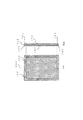
図1(a)は、本発明の第1のICカードアクセス制御体100の平面図および側面図を模式的に示す図である。なお、図1(b)は本発明と比較するために従来技術の干渉防止体1000の平面図および側面図を模式的に示している。
図2(a)は、本発明の第1のICカードアクセス制御体100を用いて二枚の非接触ICカードをカードリーダにかざした場合に干渉が起こらない様子を側面(横断面)から模式的に示した図である。なお、図2(b)は、本発明と比較するために従来技術の干渉防止体1000では実際には干渉が起こってしまう様子を側面(横断面)から模式的に示している。
First, the basic principle of the first IC card access controller of the present invention will be described.
Fig.1 (a) is a figure which shows typically the top view and side view of the 1st IC card
FIG. 2A is a schematic side view (cross section) showing that no interference occurs when two non-contact IC cards are held over a card reader using the first IC
本発明の第1のICカードアクセス制御体100は、図1(a)に示すように、導電性シートの表面側および裏面側にそれぞれ磁性シートが積層されているが、導電性シートの外周縁部分には磁性シートが積層されていない形状となっている。つまり、第1のICカードアクセス制御体100の外周縁端部分には導電性シートのみが設けられており、磁性シートは設けられておらず、磁性シートの外周縁端は導電性シートの外周縁端からやや内側となっている。
どの程度内側とするかは、カードリーダの発振磁界の強さや、非接触ICカードに内蔵されているアンテナコイルの位置などを考慮する。この点については後述する。
なお、導電性シートの大きさであるが、非接触ICカードとICカードアクセス制御体を重ね合わせた状態において、導電性シートの外周縁がアンテナコイルが設けられているエリア外周縁より外側に位置するものとする。つまり、干渉を防止するために、導電性シートが、ICカードアクセス制御体の上側に載せ置かれた非接触ICカードのアンテナコイルを覆う大きさと位置関係を有するものとする。
As shown in FIG. 1A, the first IC card
How much inside is taken into consideration is the strength of the oscillating magnetic field of the card reader, the position of the antenna coil incorporated in the non-contact IC card, and the like. This point will be described later.
Although the size of the conductive sheet, the outer peripheral edge of the conductive sheet is positioned outside the outer peripheral edge of the area where the antenna coil is provided in a state where the non-contact IC card and the IC card access control body are overlapped. It shall be. That is, in order to prevent interference, the conductive sheet has a size and a positional relationship covering the antenna coil of the non-contact IC card placed on the upper side of the IC card access control body.
一方、従来技術の干渉防止体1000は、図1(b)に示すように、導電性シート101の両面の全面に磁性シート102が積層されている。つまり、導電性シートの外周縁端部分にも磁性シートが設けられている。
上記構成の第1のICカードアクセス制御体100を二枚の非接触ICカードの間に挟み込み、改札機のカードリーダにかざした場合の電磁結合の様子を検討する。
On the other hand, as shown in FIG. 1 (b), the
The state of electromagnetic coupling when the first IC
まず初めに従来技術の干渉防止体1000の場合を説明する。
図2(b)の横断面図において、下に改札機のカードリーダ300があり、従来技術の干渉防止体1000を挟んで上側に非接触ICカード200a、下側に非接触ICカード200bが位置している。横断面となっており、アンテナコイル210はループ状のアンテナコイルの断面が模式的に示されている。
図2(b)に示すように、従来技術の干渉防止体1000では、下側に位置する非接触ICカード200bのアンテナコイル210bを通過する磁路FLbが形成され、さらに、導電性シートの外周縁端部分にも磁性シートが設けられているので導電性シートの外周縁端のやや外側を通過した磁力線が磁性シートの外周縁端から磁性シートの内側に引き込まれ、磁性シートの内側部分から再び出射し、改札機のカードリーダに戻るという磁路FLaも形成されてしまう。上側の非接触ICカード200aのアンテナコイル210aを通過する磁路となっており、結局、下側の非接触ICカード200bと上側の非接触ICカード200aの両者が改札機300のカードリーダと電磁結合して干渉が起こることとなる。このように従来技術の干渉防止体1000では実際には干渉が起こってしまうという問題が生じる。
First, the case of the
In the cross-sectional view of FIG. 2 (b), there is a
As shown in FIG. 2 (b), in the
次に、本発明の第1のICカードアクセス制御体100の場合を説明する。
図2(a)は本発明の第1のICカードアクセス制御体100によって干渉が防止される様子を側面(横断面)から模式的に示した図である。図2(a)においても、下に改札機のカードリーダがあり、本発明の第1のICカードアクセス制御体100を挟んで上側に非接触ICカード200a、下側に非接触ICカード200bが位置している。横断面となっており、アンテナコイル210はループ状のアンテナコイルの断面が模式的に示されている。
図2(a)に示すように、本発明の第1のICカードアクセス制御体100では、下側に位置する非接触ICカード200bのアンテナコイル210bを通過する磁路FLbが形成され、さらに、磁性シートの外周縁端は導電性シートのやや内側にあるため、導電性シートの外周縁端のやや外側を通過した磁力線は磁性シート102によって磁力線が引き込まれることなくそのまま第1のICカードアクセス制御体100の外側を通過して改札機のカードリーダ300へ戻る磁路FLaが形成されることとなる。この磁路FLaは上側の非接触ICカードのアンテナコイル210aを通過しない磁路となり、結局、改札機のカードリーダと電磁結合するのは下側の非接触ICカード200bのみとなり、上側の非接触ICカード200aが干渉することはない。このように本発明の第1のICカードアクセス制御体100では有効に干渉の発生を防止することができる。
以上が本発明の第1のICカードアクセス制御体の基本原理である。
Next, the case of the first IC
FIG. 2A is a diagram schematically showing from the side surface (cross section) how interference is prevented by the first IC
As shown in FIG. 2A, in the first IC card
The above is the basic principle of the first IC card access controller of the present invention.
次に、下側に位置する非接触ICカードの読み取りを感度良く可能とする働きについて検討する。磁性シートの形状は、上記のように第1のICカードアクセス制御体の上側に位置する非接触ICカードの干渉防止とともに、下側に位置する非接触ICカードの読み取り感度についても影響する。本発明の第1のICカードアクセス制御体100において、磁性シートの外周縁端を導電性シートの外周縁端からどの程度内側とするかは、カードリーダの発振磁界の強さや、非接触ICカードに内蔵されているアンテナコイルの位置などを考慮して決定する。本発明の第1のICカードアクセス制御体100では、非接触ICカードと第1のICカードアクセス制御体を重ね合わせた状態において、磁性シートの外周縁が導電性シートの外周縁より内側かつアンテナコイルが設けられているエリア内周縁より外側に位置するものとする。
Next, the function that enables reading of the non-contact IC card located on the lower side with high sensitivity will be examined. The shape of the magnetic sheet affects the reading sensitivity of the non-contact IC card located on the lower side as well as preventing interference of the non-contact IC card located on the upper side of the first IC card access control body as described above. In the first IC card
図3は、本発明の実施例1の第1のICカードアクセス制御体100と非接触ICカードのアンテナコイルとの位置関係を横断面により模式的に説明する図である。また、図4は、アンテナコイルが設けられているエリア内周縁とエリア外周縁を説明する図である。
FIG. 3 is a diagram schematically illustrating a positional relationship between the first IC
先に、図4を参照しつつ、アンテナコイルが設けられているエリア内周縁とエリア外周縁を定義しておく。図4では、形状が長方形型のアンテナコイルを例に挙げている。アンテナコイルは平面状に成型されており薄膜印刷による導線が所定回数ぐるりと渦巻き状に巻いた構成となっている。ここで、アンテナコイルが設けられているエリア内周縁とは最内周の導線が巻かれている境界であり、アンテナコイルが設けられているエリア外周縁とは最外周の導線が巻かれている境界である。図4の例では210−1がエリア内周縁、210−2がエリア外周縁となっている。なお、図3はICカードアクセス制御体および非接触ICカードを重ねた状態の断面のうち概ね左側部分のみを模式的に示したものであり、アンテナコイル210の断面が模式的に黒い四角形で示されているが、その黒い四角の左端がアンテナコイルの最外周つまりアンテナコイルが設けられているエリア外周縁であり、その黒い四角の右端がアンテナコイルの最内周つまりアンテナコイルが設けられているエリア内周縁に相当する。
First, referring to FIG. 4, the inner peripheral edge and the outer peripheral edge where the antenna coil is provided are defined. In FIG. 4, an antenna coil having a rectangular shape is taken as an example. The antenna coil is formed in a flat shape, and a conductive wire by thin film printing is wound around a predetermined number of times. Here, the inner periphery of the area where the antenna coil is provided is the boundary around which the innermost conductor is wound, and the outer periphery of the area where the antenna coil is provided is the outer periphery of the conductor. It is a boundary. In the example of FIG. 4, 210-1 is the inner periphery of the area, and 210-2 is the outer periphery of the area. FIG. 3 schematically shows only the left side of the cross section in a state where the IC card access control body and the non-contact IC card are overlapped, and the cross section of the
図3に戻り、本発明の実施例1の第1のICカードアクセス制御体100と非接触ICカードのアンテナコイルとの位置関係の説明を続ける。
本発明の第1のICカードアクセス制御体100では、図3(a)に示すように、非接触ICカードと第1のICカードアクセス制御体を重ね合わせた状態において、導電性シートの外周縁101がアンテナコイル210a,210bが設けられているエリア外周縁より外側に位置し、磁性シート102の外周縁が導電性シート101の外周縁より内側かつアンテナコイル210a,210bが設けられているエリア内周縁より外側に位置している。
このような位置関係であれば、導電性シート101の外周縁のすぐ外側を通過する磁力線は磁性シート102により引き込まれることなくそのままカードリーダ300に戻る磁路FLaを形成する。また、下側の非接触ICカード200bのやや内側から出射した磁力線は下側の磁性シート102により引き込まれ、下側の磁性シート102の外周縁端付近から再出射されてカードリーダに戻る磁路FLbを形成する。FLbは下側の非接触ICカードのアンテナコイル210bと交わり磁路となっており、電磁結合する。このように、上側の非接触ICカード200aとカードリーダの通信を遮断するとともに、下側の非接触ICカード200bとカードリーダの通信感度を上げる効果を持つ。
Returning to FIG. 3, the description of the positional relationship between the first IC card
In the first IC card
With such a positional relationship, the magnetic field lines passing just outside the outer peripheral edge of the
一方、比較のため、図3(b)のようなものを検討する。図3(b)では、導電性シートの外周縁101がアンテナコイル210a,210bが設けられているエリア外周縁より外側に位置するものの、磁性シート102の外周縁が導電性シート101の外周縁およびアンテナコイル210a,210bが設けられているエリア内周縁より内側に位置している。
この場合、導電性シート101の外周縁のすぐ外側を通過する磁力線は図3(a)と同様、磁性シート102により引き込まれることなくそのままカードリーダ300に戻る磁路FLaを形成し、下側の非接触ICカード200bのやや内側から出射した磁力線は下側の磁性シート102により引き込まれ、下側の磁性シート102の外周縁端付近から再出射されてカードリーダに戻る磁路FLbを形成するが、磁路FLaおよび磁路FLbのいずれも、非接触ICカードのアンテナコイル210a,210bと交わらない磁路となっており、電磁結合は起こらない。このように、磁性シートと非接触ICカードのアンテナコイルとの位置関係が図3(b)に示す位置関係であれば、上側の非接触ICカード200aのみならず下側の非接触ICカード200bとの通信も遮断されてしまい、ICカードアクセス制御体としては不適当なものであることが分かる。
On the other hand, for the purpose of comparison, the one shown in FIG. In FIG. 3B, the outer
In this case, the magnetic lines of force that pass just outside the outer peripheral edge of the
(実験)
次に、上記した本発明の第1のICカードアクセス制御体を試作し、カードリーダを用いて、第1のICカードアクセス制御体の上側に位置する非接触ICカードの干渉防止性能と、下側に位置する非接触ICカードの読み取り性能を確認した。
カードリーダとして、JR西日本(西日本旅客鉄道株式会社)の改札機のカードリーダ部分を用いた。
非接触ICカードとして、JR西日本(西日本旅客鉄道株式会社)が発行している「ICOCA(TM)」を用いた。
比較実験とするため、磁性シートの形状として、図5に示すような4パターンの形状を作り、それぞれの性能を確認した。なお、各パターンのICカードアクセス制御体の導電性シートの大きさは非接触ICカードと略同一の大きさである。また、各パターンのICカードアクセス制御体と非接触ICカードを重ね合わせた場合に非接触ICカード内のアンテナコイルがどのあたりに重なるのかを把握しやすいように、各パターンのICカードアクセス制御体の磁性シート上にアンテナコイルが重なる部分を薄い破線として書き込んでいる。この例ではアンテナコイル形状がアンチコリジョンタイプのいわゆる木の葉型をしている。
(Experiment)
Next, the above-described first IC card access control body of the present invention is prototyped, and using a card reader, the interference prevention performance of the non-contact IC card positioned above the first IC card access control body is The reading performance of the non-contact IC card located on the side was confirmed.
As the card reader, the card reader portion of the ticket gate of JR West (West Japan Railway Company) was used.
As the non-contact IC card, “ICOCA (TM)” issued by JR West (West Japan Railway Company) was used.
In order to make a comparative experiment, four patterns as shown in FIG. 5 were made as the shape of the magnetic sheet, and the respective performances were confirmed. The size of the conductive sheet of the IC card access control body of each pattern is substantially the same as that of the non-contact IC card. In addition, when the IC card access control body of each pattern and the non-contact IC card are overlapped, the IC card access control body of each pattern is easy to grasp where the antenna coil in the non-contact IC card overlaps. The portion where the antenna coil overlaps on the magnetic sheet is written as a thin broken line. In this example, the antenna coil has an anti-collision type so-called tree leaf shape.
パターン1は、従来技術の干渉防止体1000と同様、導電性シートの全面に磁性シートを積層した形状となっている。
パターン2は、パターン1の磁性シートの外周縁を5mm幅にて取り除いたものである。このパターン2は、本発明の第1のICカードアクセス制御体100の磁性シートの条件を備えたパターンとなっており、磁性シート102の外周縁が導電性シート101の外周縁より内側かつアンテナコイル210a,210bが設けられているエリア内周縁(パターン中に破線で示した木の葉型の内周縁)より外側に位置しているものとなっている。
パターン3は、パターン1のうち、非接触ICカードと重ね合わせた場合に非接触ICカードのアンテナコイルが重なる部分の磁性シートを除いたものとなっている。つまり、アンチコリジョンタイプのいわゆる木の葉型にくり抜かれたものとなっている。
パターン4は、パターン1の磁性シートの内側を取り除いたものとなっており、非接触ICカードと重ね合わせた場合に非接触ICカードのアンテナコイルと重なる部分の内側を取り除いたものとなっている。
上記4つのパターンのうち、パターン2が本発明の実施例1にかかる第1のICカードアクセス制御体の一構成例となっている。つまり、導電性シートの外周縁部分には磁性シートを積層しない形状となっており、また、導電性シートの外周縁がアンテナコイルが設けられているエリア外周縁より外側に位置し、磁性シートの外周縁が導電性シートの外周縁より内側かつアンテナコイルが設けられているエリア内周縁より外側に位置しているものとなっている。
The
The
The pattern 4 is obtained by removing the inner side of the magnetic sheet of the
Of the above four patterns,
図6は、非接触ICカードの読み取り実験の方法を説明する図である。
上側の非接触ICカードの通信遮断性能実験と下側の非接触ICカードの通信性能実験を同時に行うことは難しいので、それぞれ別々に行った。
図6(a)は上側の非接触ICカードの通信遮断性能実験の方法を説明する図である。本発明の第1のICカードアクセス制御体100の上側(カードリーダとは反対側)に非接触ICカード200aを載せ置き、そのまま、カードリーダに対して近づけて行き、カードリーダによって非接触ICカード200aが読み取られた時点で通信遮断が失敗したと判定する。つまり、この非接触ICカード200aが読み取られた時点の距離(反応距離)を通信遮断性能と評価する。
図6(b)は下側の非接触ICカードの通信性能実験の方法を説明する図である。本発明の第1のICカードアクセス制御体100の下側(カードリーダ側)に非接触ICカード200bを持ち、そのまま、カードリーダに対して近づけて行き、カードリーダによって非接触ICカード200bが読み取られた時点で通信が成功したと判定する。つまり、この非接触ICカード200bが読み取られた時点の距離(反応距離)を通信性能と評価する。
FIG. 6 is a diagram for explaining a method of a non-contact IC card reading experiment.
Since it is difficult to simultaneously perform the communication blocking performance experiment of the upper non-contact IC card and the lower non-contact IC card, they were performed separately.
FIG. 6A is a diagram for explaining a method of a communication cutoff performance experiment for the upper non-contact IC card. The
FIG. 6B is a diagram for explaining a communication performance experiment method for the lower non-contact IC card. The
図7は、上側の非接触ICカードの通信遮断性能実験と下側の非接触ICカードの通信性能実験の結果を示す図である。
縦軸は反応距離である。横軸は磁性シートのパターンであり、左からパターン1、パターン2、パターン3、パターン4となっている。
各パターンにおいて、左側の棒グラフが上側の非接触ICカードの通信遮断性能を示すグラフであり、右側の棒グラフが下側の非接触ICカードの通信性能を示すグラフである。
FIG. 7 is a diagram showing the results of the communication blocking performance experiment for the upper non-contact IC card and the communication performance experiment for the lower non-contact IC card.
The vertical axis represents the reaction distance. The horizontal axis is the pattern of the magnetic sheet, which is
In each pattern, the left bar graph is a graph showing the communication cutoff performance of the upper non-contact IC card, and the right bar graph is a graph showing the communication performance of the lower non-contact IC card.
図7のパターン1の結果より以下のことが確認できた。下側の非接触ICカードの通信性能は約6.5cmであり、第1のICカードアクセス制御体100の下側(カードリーダ側)に位置する非接触ICカードは性能良くカードリーダによって読み取られることが分かった。一方、上側の非接触ICカードの通信性能は約3.5cmであり、第1のICカードアクセス制御体100の上側(カードリーダとは反対側)に位置する非接触ICカードについては遮断性能は働かず、カードリーダによって読み取られてしまうことが分かった。
The following could be confirmed from the result of
図7のパターン2の結果より以下のことが確認できた。下側の非接触ICカードの通信性能は約5cmであり、第1のICカードアクセス制御体100の下側(カードリーダ側)に位置する非接触ICカードは性能良くカードリーダによって読み取られることが分かった。一方、上側の非接触ICカードにはまったく反応せずに読み取りはできなかった(遮断)。つまり、第1のICカードアクセス制御体100の上側(カードリーダとは反対側)に位置する非接触ICカードについては遮断性能が働いて干渉することがないことが確認された。
The following could be confirmed from the result of
図7のパターン3の結果より以下のことが確認できた。上側の非接触ICカードにはまったく反応せずに読み取りはできず(遮断)、また、下側の非接触ICカードに対してはエラーが発生して読み取りができなかった(エラー)。つまり、第1のICカードアクセス制御体100の上側(カードリーダとは反対側)に位置する非接触ICカードについては遮断性能が働いて干渉することがないものの、第1のICカードアクセス制御体100の下側(カードリーダ側)に位置する非接触ICカードについて通信性能が発揮できないことが確認された。この現象は下側の非接触ICカードのアンテナコイルの背後に磁性シートがなく導電性シート101のみがあると読み取るべき非接触ICカードのアンテナコイル210を通過した発振磁界がそのまま導電性シート101に相殺されてしまい、カードリーダ側に戻る磁路が形成されないために生じる。磁性シート102を設けておけば発振磁界を引き込んでカードリーダ側に返すための磁路の形成が可能となるが、パターン3では磁性シートの形状が当該磁路の形成を助ける形状とはなっていない。
The following could be confirmed from the result of
図7のパターン4の結果より以下のことが確認できた。下側の非接触ICカードの通信性能は約4.5cmであり、第1のICカードアクセス制御体100の下側(カードリーダ側)に位置する非接触ICカードは性能良くカードリーダによって読み取られることが分かった。一方、上側の非接触ICカードの通信性能は約0.5cmであり、第1のICカードアクセス制御体100の上側(カードリーダとは反対側)に位置する非接触ICカードについては遮断性能は不十分であり、カードリーダによって読み取られてしまうことが分かった。図2(b)に示す状態が発生していると考えられ、第1のICカードアクセス制御体100の上側(カードリーダとは反対側)に位置する非接触ICカードについては遮断性能は十分とは言えないことが分かった。
The following could be confirmed from the result of pattern 4 in FIG. The communication performance of the lower non-contact IC card is about 4.5 cm, and the non-contact IC card located on the lower side (card reader side) of the first IC
以上の実験から、従来技術の干渉防止体と同様の磁性シートの形状であれば、第1のICカードアクセス制御体としての上側の非接触ICカードに対する通信遮断性能が不十分となり、アンテナコイルに対応する位置の磁性シートを取り除いた形状であれば、下側の非接触ICカードに対する通信性能が十分発揮されず、アンテナコイルのすぐ内側を取り除いた形状の磁性シートでも上側の非接触ICカードに対する通信遮断性能は不十分であることが分かった。
本発明の第1のICカードアクセス制御体のように、パターン2の形状の磁性シートとすると、第1のICカードアクセス制御体としての上側の非接触ICカードに対する通信遮断性能も十分に発揮され、下側の非接触ICカードに対する通信性能も十分発揮されることが確認できた。
From the above experiment, if the shape of the magnetic sheet is the same as that of the interference prevention body of the prior art, the communication blocking performance for the upper non-contact IC card as the first IC card access control body becomes insufficient, and the antenna coil If the magnetic sheet in the corresponding position is removed, the communication performance for the lower non-contact IC card is not sufficiently exerted, and the magnetic sheet with the shape just removed from the inner side of the antenna coil is not compatible with the upper non-contact IC card. It was found that the communication interruption performance was insufficient.
If the magnetic sheet having the
次に、磁性シートの外周縁端を導電性シートの外周縁端からどの程度内側とすれば良いかについて実験した。どの程度内側とするかは、カードリーダの発振磁界の強さや、非接触ICカードに内蔵されているアンテナコイルの位置、導電性シートとICカードの大きさの関係などを考慮する必要がある。図7は導電性シートの外周縁端と磁性シートの外周縁端との距離を変化させつつ、上側の非接触ICカードに対する通信遮断性能と下側の非接触ICカードに対する通信性能を計測した結果を示す図である。カードリーダは上記と同様、JR西日本(西日本旅客鉄道株式会社)の改札機のカードリーダを用いた。非接触ICカードも実施例1と同様、JR西日本(西日本旅客鉄道株式会社)が発行している「ICOCA(TM)」を用いた。 Next, an experiment was conducted on how much the outer peripheral edge of the magnetic sheet should be inside the outer peripheral edge of the conductive sheet. It is necessary to consider how much the inside is to be taken into consideration, such as the strength of the oscillating magnetic field of the card reader, the position of the antenna coil built in the non-contact IC card, the relationship between the size of the conductive sheet and the IC card. FIG. 7 shows the result of measuring the communication blocking performance for the upper non-contact IC card and the communication performance for the lower non-contact IC card while changing the distance between the outer peripheral edge of the conductive sheet and the outer peripheral edge of the magnetic sheet. FIG. As above, the card reader used was a ticket reader of JR West Japan (West Japan Railway Company). Similarly to Example 1, the non-contact IC card used was “ICOCA (TM)” issued by JR West (West Japan Railway Company).
図8に見るように、上側の非接触ICカードに対する通信遮断性能は、磁性シートの外周縁端を導電性シートの外周縁端から3ミリ内側となったあたりから発揮され始め、5ミリ以上では精度よく通信が遮断された。一方、下側の非接触ICカードに対する通信性能は、磁性シートの外周縁端を導電性シートの外周縁端から5ミリあたりまでは精度良く発揮されていたが、9ミリ内側となった時点では通信性能が発揮できないことが分かった。一例として実験したカードリーダと非接触ICカードの組み合わせでは、上側の非接触ICカードに対する通信遮断性能と下側の非接触ICカードに対する通信性能がともに確保される範囲として、3〜7ミリの範囲が好ましく、5ミリ程度がもっとも安定していることが確認できた。
なお、本実験におけるパターン2の第1のICカードアクセス制御体であれば、今回実験に使用したJR西日本の「ICOCA」に採用されているサイバネティック規格のアンチコリジョンコイルアンテナ(いわゆる木の葉型コイルアンテナ)や、電子マネーとして普及している「EDi(エディ)」を始め広く一般に採用されている長方形のコイルアンテナのいずれであっても適用することができ、汎用性が高いものとなっている。
As shown in FIG. 8, the communication blocking performance for the upper non-contact IC card starts to be exhibited when the outer peripheral edge of the magnetic sheet is 3 mm inside from the outer peripheral edge of the conductive sheet. Communication was interrupted with high accuracy. On the other hand, the communication performance with respect to the lower non-contact IC card was exhibited accurately from the outer peripheral edge of the magnetic sheet up to about 5 mm from the outer peripheral edge of the conductive sheet, but when it became 9 mm inside It turned out that communication performance cannot be demonstrated. As an example, the combination of the card reader and the non-contact IC card tested as an example is a range of 3 to 7 mm as a range in which both the communication blocking performance for the upper non-contact IC card and the communication performance for the lower non-contact IC card are secured. It is preferable that about 5 mm is most stable.
In the case of the first IC card access control body of
実施例2の第1のICカードアクセス制御体は、本発明の第1のICカードアクセス制御体としての性能劣化を抑えつつ、コストを低減するため、磁性シートの面積を小さく工夫したものである。
実施例1にかかる第1のICカードアクセス制御体は磁性シートの形状が導電性シートの外周縁部分には磁性シートを積層しない形状となっていたが、実施例2にかかる第1のICカードアクセス制御体は磁性シートの形状において、非接触ICカードのアンテナコイルが設けられているエリアより内側のエリアに相当する部分を取り除いた形状としている。
The first IC card access control body of Example 2 is a device in which the area of the magnetic sheet is devised to reduce costs while suppressing performance deterioration as the first IC card access control body of the present invention. .
In the first IC card access controller according to the first embodiment, the shape of the magnetic sheet is such that the magnetic sheet is not laminated on the outer peripheral edge portion of the conductive sheet. The access control body is formed by removing a portion corresponding to the area inside the area where the antenna coil of the non-contact IC card is provided in the shape of the magnetic sheet.
図9は、実施例2の第1のICカードアクセス制御体の磁性シートの形状パターンを模式的に示す図である。パターン5が実施例2の第1のICカードアクセス制御体の磁性シートの形状パターンである。分かりやすいように、実施例1の図5で用いたパターン1を再掲している。
なお、図9においても、各パターンの第1のICカードアクセス制御体と非接触ICカードを重ね合わせた場合に非接触ICカード内のアンテナコイルがどのあたりに重なるのかを把握しやすいように、各パターンの第1のICカードアクセス制御体の磁性シート上にアンテナコイルが重なる部分を薄い破線として書き込んでいる。この例ではアンテナコイル形状がアンチコリジョンタイプのいわゆる木の葉型をしている。
FIG. 9 is a diagram schematically illustrating the shape pattern of the magnetic sheet of the first IC card access control body according to the second embodiment.
In FIG. 9 also, when the first IC card access control body of each pattern and the non-contact IC card are overlapped, it is easy to grasp where the antenna coil in the non-contact IC card overlaps. The portion where the antenna coil overlaps is written as a thin broken line on the magnetic sheet of the first IC card access control body of each pattern. In this example, the antenna coil has an anti-collision type so-called tree leaf shape.
実施例2のパターン5は、実施例1の図5のパターン2と同様、パターン1の磁性シートの外周縁を5mm幅にて取り除いたものとなっているが、アンテナコイルに相当するエリア(いわゆる木の葉型形状のエリア)の内側縁から5mm幅程度のマージンを残し、その内側の部分を取り除いた形状となっている。つまり、実施例2のパターン5の磁性シートの形状は、ICカードアクセス制御体と非接触ICカードを重ね合わせた状態において、カードリーダから上向きに放射された磁力線を、下側にある非接触ICカードのアンテナコイルのやや内側に位置する5mm幅程度のマージン部分から引き込んで磁性シートの外周縁から外側へ再放射する形状となっている。このパターン5の磁性シートの形状により形成が促進される磁路は非接触ICカードのアンテナコイルと交わるものとなっており、下側(カードリーダ側)にある非接触ICカードの通信性能を確保するものとなっている。実施例1のパターン2と比べ、中央部分には磁性シートがないので、磁力線の引き込みが小さくなり通信性能がやや劣るが、アンテナコイルのやや内側では磁力線の引き込みが可能となっているので通信性能を確保することは可能である。上側(カードリーダとは反対側)の非接触ICカードに対する通信遮断性能については、導電性シートの外周縁には磁性シートが設けられていないので実施例1で説明した図2(b)の外周縁からの磁力線の回り込みがなく、上側(カードリーダとは反対側)にある非接触ICカードの通信遮断性能を確保するものとなっている。
The
(実験)
次に、上記したパターン5の磁性シートの形状を持つ第1のICカードアクセス制御体を試作し、カードリーダを用いて、第1のICカードアクセス制御体の上側に位置する非接触ICカードの干渉防止性能と、下側に位置する非接触ICカードの読み取り性能を確認した。
カードリーダは実施例1と同様、JR西日本(西日本旅客鉄道株式会社)の改札機のカードリーダを用いた。
非接触ICカードも実施例1と同様、JR西日本(西日本旅客鉄道株式会社)が発行している「ICOCA(TM)」を用いた。
(Experiment)
Next, the first IC card access control body having the shape of the magnetic sheet of the
As in Example 1, a card reader of a ticket gate of JR West (West Japan Railway Company) was used.
Similarly to Example 1, the non-contact IC card used was “ICOCA (TM)” issued by JR West (West Japan Railway Company).
図10は、図9に示したパターン5の磁性シートを持つ第1のICカードアクセス制御体を用いた実験結果を示す図である。
比較するため、実施例1のパターン1、パターン2の磁性シートの形状を持つ第1のICカードアクセス制御体についてもプロットした。
図9のパターン5の結果より以下のことが確認できた。下側の非接触ICカードの通信性能は約4cmであり、第1のICカードアクセス制御体100の下側(カードリーダ側)に位置する非接触ICカードは性能良くカードリーダによって読み取られることが分かった。一方、上側の非接触ICカードもパターン2と同様、読み取りはできず、第1のICカードアクセス制御体100の上側(カードリーダとは反対側)に位置する非接触ICカードについては遮断性能が働いて干渉することがないことが確認された。
FIG. 10 is a diagram showing an experimental result using the first IC card access control body having the magnetic sheet of the
For comparison, the first IC card access control body having the shape of the magnetic sheet of
The following could be confirmed from the result of
実施例3にかかる第1のICカードアクセス制御体は、実施例1と同様に磁性シートの形状を導電性シートの外周縁部分には磁性シートを積層しない形状とするが、磁性シートの当該外周縁部分に非導電性材料からなる帯体を設けたものである。 The first IC card access control body according to the third embodiment is similar to the first embodiment in that the magnetic sheet has a shape in which the magnetic sheet is not laminated on the outer peripheral edge portion of the conductive sheet. A belt made of a non-conductive material is provided at the peripheral portion.
図11は、実施例3にかかる第1のICカードアクセス制御体の平面図および側面図を模式的に示す図である。図1(a)と同様、磁性シート102の形状は導電性シートの外周縁部分には磁性シートを積層しない形状となっているが、空隙のままとせず、プラスチックなどの非導電性材料からなる帯体103を設けたものとしている。非導電性材料は磁性シートのごとく磁力線を引き込んで再放射するという能力はなく、導電性シートのやや外側を通過する磁力線を引き込むことはない。
FIG. 11 is a schematic diagram of a plan view and a side view of the first IC card access control body according to the third embodiment. As in FIG. 1A, the shape of the
図12は、実施例3にかかる第1のICカードアクセス制御体100を用いて二枚の非接触ICカードをカードリーダにかざした場合に干渉が起こらない様子を側面から模式的に示した図である。図2(a)と同様、非導電性の帯体103のために磁性シートの外周縁端は導電性シートのやや内側となっているため、導電性シートの外周縁端のやや外側を通過した磁力線は磁性シート102によって磁力線が引き込まれることなくそのまま第1のICカードアクセス制御体100の外側を通過して改札機のカードリーダ300へ戻る磁路FLaが形成されることとなる。この磁路FLaは上側の非接触ICカードのアンテナコイル210aを通過しない磁路となり、結局、改札機のカードリーダと電磁結合するのは下側の非接触ICカード200bのみとなり、上側の非接触ICカード200aが干渉することはない。このように実施例3の第1のICカードアクセス制御体も実施例1の第1のICカードアクセス制御体と同様、有効に干渉の発生を防止することができる。
FIG. 12 is a diagram schematically showing from the side how interference does not occur when two non-contact IC cards are held over a card reader using the first IC
実施例4として本発明の第2のICカードアクセス制御体の例を示す。
本発明の第2のICカードアクセス制御体は、基板の一方の面をスキミング防止面とし、他方の面をICカード利用面としたものである。
実施例4にかかる第2のICカードアクセス制御体は、基板となる導電性シートと、導電性シートのICカード利用面に積層した磁性シートを備え、磁性シートの形状を、導電性シートの外周縁部分には磁性シートを積層せずに導電性シートの形状より小さい形状としている。磁性シートが積層されていない面をスキミング防止面とし、磁性シートが積層されている面をICカード利用面とする。
As a fourth embodiment, an example of the second IC card access control body of the present invention will be shown.
In the second IC card access control body of the present invention, one surface of the substrate is a skimming prevention surface and the other surface is an IC card utilization surface.
A second IC card access control body according to Example 4 includes a conductive sheet serving as a substrate and a magnetic sheet laminated on the IC card utilization surface of the conductive sheet, and the shape of the magnetic sheet is adjusted to the outside of the conductive sheet. A magnetic sheet is not laminated on the peripheral portion, and the shape is smaller than that of the conductive sheet. The surface on which the magnetic sheet is not laminated is defined as a skimming prevention surface, and the surface on which the magnetic sheet is laminated is defined as an IC card utilization surface.
図13は、本発明の第2のICカードアクセス制御体500のスキミング防止面、側面、ICカード利用面を模式的に示す図である。
図13に示すように第2のICカードアクセス制御体500は、基板となる導電性シート501と、当該導電性シート501の一方の面(ICカード利用面)に磁性シート502を積層した構造となっている。
実施例4に示す例では磁性シート502の形状に工夫を加えている。基板となっている導電性シート501の外周縁部分には磁性シートを積層せず、磁性シート502の形状を基板となる導電性シート501より小さい形状としている。つまり、ICカード利用面において外周縁部分には磁性シート502は積層されておらず、やや内側部分から中央にかけて磁性シート502が積層されている構造となっている。なお、スキミング防止面には磁性シート502が積層されておらず、基板である導電性シート501が剥き出しとなっている。
FIG. 13 is a diagram schematically showing a skimming prevention surface, a side surface, and an IC card utilization surface of the second IC
As shown in FIG. 13, the second IC card
In the example shown in Example 4, the shape of the
ここで、基板となる導電性シート501の大きさと磁性シート502の大きさの関係は、実施例1と同様、非接触ICカード200と第2のICカードアクセス制御体500を重ね合わせた状態において、導電性シート501の外周縁がアンテナコイルが設けられているエリア外周縁211より外側に位置し、磁性シート502の外周縁が導電性シート502の外周縁より内側かつアンテナコイルが設けられているエリア内周縁212より外側に位置したものとする。
磁性シート502の形状について上記のような工夫を加えることにより、実施例1に示したように、カードリーダがICカード利用面側にある場合には磁性シートによって磁力線を引き込んで再放射を支援する効果を持たせるとともに、カードリーダがスキミング防止面側にある場合にはICカード利用面側の磁性シートの外周縁から磁力線を引き込んで再放射するという現象が起こらないように防止する効果を狙っている。
Here, the relationship between the size of the
By adding the above-described device to the shape of the
実施例4の第2のICカードアクセス制御体500には基本的な使用態様は少なくとも3通りある。図14は第2のICカードアクセス制御体500の基本的なそれぞれの使用態様を模式的に示した図である。
図14(a)は第1の使用態様を示している。第1の使用態様は少なくとも一枚の非接触ICカードをスキミング防止面に沿わせるように保持し、非接触ICカードのスキミング防止を図る使用態様である。
図14(b)は第2の使用態様を示している。第2の使用態様は少なくとも一枚の非接触ICカードをICカード利用面に沿わせるように保持し、非接触ICカードのスキミング防止とカード利用支援の2つの制御を図る使用態様である。
図14(c)は第3の使用態様を示している。第3の使用態様は少なくとも二枚の非接触ICカードのうち一枚をスキミング防止面に、他の一枚をICカード利用面にそれぞれ沿わせて保持し、非接触ICカードのスキミング防止とICカード利用面側のICカードの利用支援の2つの制御を図る使用態様である。
それぞれの使用態様において非接触ICカードとICカードアクセス制御体を沿わせた状態で皮製や布製などの一般のカードケースに入れて使用する。
The second IC
FIG. 14A shows a first usage mode. The first usage mode is a usage mode in which at least one non-contact IC card is held along the skimming prevention surface to prevent skimming of the non-contact IC card.
FIG. 14B shows a second usage mode. The second usage mode is a usage mode in which at least one non-contact IC card is held along the IC card usage surface, and two controls, prevention of skimming of the non-contact IC card and card usage support, are performed.
FIG. 14C shows a third usage mode. In the third usage mode, one of at least two non-contact IC cards is held along the skimming prevention surface and the other one is held along the IC card use surface to prevent skimming of the non-contact IC card and the IC. This is a usage mode in which two controls for use support of an IC card on the card usage side are performed.
In each usage mode, the non-contact IC card and the IC card access control body are put in a general card case made of leather or cloth and used.
まず第1の使用態様について説明する。
第1の使用態様は、一枚の非接触ICカードをスキミング防止面に沿わせるように保持し、カードケース700に収めた状態のまま、例えば胸ポケットなどに入れて持つ。第1の使用態様ではカードケースの持ち方は自由であり、図15(a)に示すようにスキミング防止面側を外表面側に向けて持っても良く、図15(b)に示すようにICカード利用面側を外表面側に向けて持っても良い。いずれの持ち方でもスキミング防止効果が得られる。
First, the first usage mode will be described.
In the first use mode, a non-contact IC card is held so as to be along the skimming prevention surface, and held in the
図16は第1の使用態様におけるスキミング防止効果を模式的に示した図である。なお、図16は横断面となっており、アンテナコイル210はループ状のアンテナコイルの断面として模式的に四角形で示されている。なお、211はアンテナコイルのエリアの外周縁であり、212はアンテナコイルのエリアの内周縁である。
FIG. 16 is a diagram schematically showing the skimming prevention effect in the first usage mode. FIG. 16 shows a cross section, and the
図16(a)はスキミング防止面側が外表面に位置した場合の磁力線の流れを示している。第1の使用態様においてスキミング防止面が外表面に位置した場合は非接触ICカード500がカードリーダ300に対向する位置にある。しかし、実施例1において説明したように、非接触ICカード200の背後に導電性シート500が密着して存在する場合、非接触ICカード200とカードリーダ300とはうまく電磁結合できない。この現象は読み取るべき非接触ICカードのアンテナコイル210を通過した発振磁界(FLb)がそのまま導電性シート501に相殺されてしまい、カードリーダ側に戻る磁路(点線で示した磁路)が形成されないために生じる。このように第1の使用態様においてスキミング防止面を外表面側となるように持っている場合は外部からスキミングを試行されてもスキミングを防止する効果が得られている。
FIG. 16A shows the flow of magnetic lines of force when the skimming prevention surface side is located on the outer surface. In the first usage mode, when the skimming prevention surface is located on the outer surface, the
次に、図16(b)はICカード利用面が外表面に位置した場合の磁力線の流れを示している。第1の使用態様においてICカード利用面が外表面に位置した場合は導電性シート501が非接触ICカード200とカードリーダ300との間にある。実施例1において説明したように、磁性シート502はカードリーダ300から放射された磁力線(FLb)を引き込んで再放射するが、導電性シート501の存在により、非接触ICカード200とカードリーダ300が電磁結合できない。このように第1の使用態様においてICカード利用面を外表面側となるように持っている場合に外部からスキミングを試行されてもスキミングを防止する効果が得られている。
以上、第1の使用態様では、図16(a)、図16(b)のいずれの持ち方をしていてもスキミング防止効果が得られることが分かる。
Next, FIG. 16B shows the flow of magnetic lines of force when the IC card utilization surface is located on the outer surface. In the first usage mode, when the IC card utilization surface is located on the outer surface, the
As described above, in the first usage mode, it can be understood that the skimming prevention effect can be obtained regardless of the holding method shown in FIGS. 16 (a) and 16 (b).
(実験)
次に、実際に本発明の第2のICカードアクセス制御体を試作し、第1の使用態様の場合のスキミング防止性能を実験により確認した。カードリーダとして、JR西日本(西日本旅客鉄道株式会社)の改札機のカードリーダ部分を用いた。非接触ICカードとして、JR西日本(西日本旅客鉄道株式会社)が発行している「ICOCA(TM)」を用いた。磁性シートの形状として、図5に示したパターン2を採用した。
(Experiment)
Next, the second IC card access control body of the present invention was actually manufactured as a prototype, and the skimming prevention performance in the case of the first usage mode was confirmed by experiments. As the card reader, the card reader portion of the ticket gate of JR West (West Japan Railway Company) was used. As the non-contact IC card, “ICOCA (TM)” issued by JR West (West Japan Railway Company) was used. The
実験ではスキミング用のカードリーダに見立ててカードリーダ300を設置した。カードケース700には第2のICカードアクセス制御体500と非接触ICカード200を入れ、非接触ICカード200は第2のICカードアクセス制御体500のスキミング防止面に沿わせた。そしてスキミング防止面がカードリーダ300側(図16(a)に相当する関係)となるようにカードケース700を持ってカードリーダ300に徐々に近づけて行き、カードリーダ300が非接触ICカード200との間で読み取りができた時点の反応距離を計測する第1の測定と、ICカード利用面がカードリーダ300側(図16(b)に相当する関係)となるようにカードケース700を持ってカードリーダ300に徐々に近づけて行き、カードリーダ300が非接触ICカード200との間で読み取りができた時点の反応距離を計測する第2の測定を行なった。
In the experiment, the
図17に第1の使用態様の場合の確認実験の結果を示す。
図17の左側に示すように、スキミング防止面側の反応距離は0、つまり、カードケース700をカードリーダ300にピッタリ密着させるまで近づけても非接触ICカード200の情報を読み取ることはできなかった。
次に、図17の右側に示すように、ICカード利用面側の反応距離も0、つまり、カードケース700をカードリーダ300にピッタリ密着させるまで近づけても非接触ICカード200の情報を読み取ることはできなかった。
以上から、本発明の第2のICカードアクセス制御体500は、第1の使用態様においていずれの持ち方をしても良好なスキミング防止効果が確認できた。
FIG. 17 shows the result of the confirmation experiment in the case of the first usage mode.
As shown on the left side of FIG. 17, the reaction distance on the skimming prevention surface side is 0, that is, the information on the
Next, as shown on the right side of FIG. 17, the reaction distance on the IC card utilization surface side is also 0, that is, the information of the
From the above, it was confirmed that the second IC
次に、第2の使用態様について説明する。
第2の使用態様は、非接触ICカードをICカード利用面に沿わせるように保持し、非接触ICカード200を使用しないときは図18(a)のようにスキミング防止面を外表面側となるようにカードケース700を胸ポケットなどに入れて持ち、非接触ICカード200を使用するときは図18(b)のようにICカード利用面側を交通機関の改札機や金融機関のATMのカードリーダにかざすようにカードケース700を持つ。第2の使用態様によれば非接触ICカード200を使用しないときはスキミング防止効果が得られ、非接触ICカー200を使用するときはICカード利用支援効果が得られる。
Next, the second usage mode will be described.
In the second usage mode, the non-contact IC card is held along the IC card utilization surface. When the
図19は第2の使用態様におけるスキミング防止効果とICカード利用支援効果を模式的に示した図である。なお、図19は図16と同様、横断面となっており、アンテナコイル210はループ状のアンテナコイルの断面として模式的に四角形で示されている。なお、211はアンテナコイルのエリアの外周縁であり、212はアンテナコイルのエリアの内周縁である。
FIG. 19 is a diagram schematically showing a skimming prevention effect and an IC card utilization support effect in the second usage mode. Note that FIG. 19 has a cross section similar to FIG. 16, and the
図19(a)は第2の使用態様において、スキミング防止面側のカードリーダ300から放射された磁力線の流れを示している。第2の使用態様においてスキミング防止面が外表面に位置した場合は導電性シート501がカードリーダ300に対向する位置にあり、カードリーダ300から放射された磁路FLbが導電性素材の導電性シート501により遮断される。この現象は、磁力線が導電性素材に吸収されて熱エネルギーに変換されると説明することができ、また、入射する磁力線に対して導電性シートから同量逆位相の磁力線が誘起され、両者が打ち消し合って見かけ上、磁力線が導電性シート501表面で遮断されると説明することもできる。
このように、本発明の第2の使用態様においてスキミング防止面側からスキミング用のカードリーダにより不正読み取りを図っても非接触ICカード200を読み取ることはできず、スキミング防止効果が得られる。
FIG. 19A shows the flow of magnetic lines of force radiated from the
As described above, in the second usage mode of the present invention, even if illegal reading is performed from the skimming prevention surface side by the card reader for skimming, the
図19(b)は第2の使用態様において非接触ICカード200を利用すべく、交通機関の改札機や金融機関のATMのカードリーダなどにICカード利用面側からかざした場合の磁力線の流れを示している。第2の使用態様においてICカード利用面側からカードリーダ300にかざした場合は非接触ICカード200がカードリーダ300に対向する位置にあり、実施例1において説明したように、磁性シート502はカードリーダ300から放射された磁力線(FLb)を引き込んで再放射するので、非接触ICカード200のアンテナコイル210を通過する磁路の形成が支援され、非接触ICカード200とカードリーダ300が電磁結合する。このように第2の使用態様においてICカード利用面側からカードリーダ300にかざした場合はICカードの利用支援効果が得られる。
FIG. 19B shows the flow of magnetic lines of force when the IC card is used over the ticket gate of a transportation facility or an ATM card reader of a financial institution in order to use the
(実験)
次に、第1の使用態様の実験と同様、実際に本発明の第2のICカードアクセス制御体を用いて、第2の使用態様の場合のスキミング防止効果およびICカード利用支援効果を実験により確認した。
実験ではカードリーダに見立ててカードリーダ300を設置した。カードケース700には第2のICカードアクセス制御体500と非接触ICカード200を入れ、非接触ICカード200をICカード利用面に沿わせた。
スキミング防止面がカードリーダ300側(図19(a)に相当する関係)となるようにカードケース700を持ってカードリーダ300に徐々に近づけて行き、カードリーダ300が非接触ICカード200との間で読み取りができた時点の反応距離を計測する第1の測定と、ICカード利用面がカードリーダ300側(図19(b)に相当する関係)となるようにカードケース700を持ってカードリーダ300に徐々に近づけて行き、カードリーダ300が非接触ICカード200との間で読み取りができた時点の反応距離を計測する第2の測定を行なった。
(Experiment)
Next, as in the experiment of the first usage mode, the skimming prevention effect and the IC card utilization support effect in the second usage mode are actually tested by using the second IC card access controller of the present invention. confirmed.
In the experiment, the
Gradually approach the
図20に第2の使用態様の場合の確認実験の結果を示す。
図20の左側に示すように、スキミング防止面側の反応距離は0、つまり、カードケース700をカードリーダ300にピッタリ密着させるまで近づけても非接触ICカード200の情報を読み取ることはできなかった。
次に、図20の右側に示すように、ICカード利用面側の反応距離は約50mmであった。つまり、カードケース700をカードリーダ300に50mm以内に近づけると非接触ICカード200の情報を読み取ることができた。
以上から、本発明の第2のICカードアクセス制御体500は、第2の使用態様においてスキミング防止面を外表面に向けて保持している状態では良好なスキミング防止効果が得られることが確認でき、ICカードを利用するためにICカード利用面側からカードリーダにかざすと良好なICカード利用支援効果が得られることが確認できた。
FIG. 20 shows the result of the confirmation experiment in the case of the second usage mode.
As shown on the left side of FIG. 20, the reaction distance on the skimming prevention surface side is 0, that is, the information on the
Next, as shown on the right side of FIG. 20, the reaction distance on the IC card utilization surface side was about 50 mm. That is, when the
From the above, it can be confirmed that the second IC
次に、第3の使用態様について説明する。
第3の使用態様は、少なくとも二枚の非接触ICカードのうち一枚をスキミング防止面に、他の一枚をICカード利用面にそれぞれ沿わせて保持し、スキミング防止面側に沿わせた非接触ICカードのスキミング防止とICカード利用面側に沿わせた非接触ICカードの利用支援の制御を図る使用態様である。例えば、金融機関の非接触ICカード200Aをスキミング防止面に沿わせ、交通機関の非接触ICカード200BをICカード利用面に沿わせる。非接触ICカード200A、Bのいずれも使用しないときは図21(a)のようにスキミング防止面を外表面側となるようにカードケース700を胸ポケットなどに入れて持つとスキミング防止効果が得られる。また、交通機関の非接触ICカード200Bを使用するときは図21(b)のようにICカード利用面側を交通機関の改札機のカードリーダにかざすようにカードケース700を持つと非接触ICカード200BのICカード利用支援効果が得られる。なお、この例では非接触ICカード200Aを使用するときは非接触ICカード200Aをカードケース700から取り出して使用することとなる。
Next, the third usage mode will be described.
In the third usage mode, one of at least two contactless IC cards is held along the skimming prevention surface, and the other one is held along the IC card use surface, and is placed along the skimming prevention surface side. This is a usage mode in which skimming prevention of the non-contact IC card and control of use support of the non-contact IC card along the IC card use surface side are performed. For example, the
図22は第3の使用態様におけるスキミング防止効果とICカード利用支援効果を模式的に示した図である。なお、図22は図16と同様、横断面となっており、アンテナコイル210はループ状のアンテナコイルの断面として模式的に四角形で示されている。なお、211はアンテナコイルのエリアの外周縁であり、212はアンテナコイルのエリアの内周縁である。
FIG. 22 is a diagram schematically showing the skimming prevention effect and the IC card utilization support effect in the third usage mode. Note that FIG. 22 has a transverse cross section, similar to FIG. 16, and the
図22(a)は第3の使用態様において、スキミング防止面側のカードリーダ300から放射された磁力線の流れを示している。スキミング防止面に沿わせた非接触ICカード200Aがカードリーダ300に対向する位置にある。しかし、第1の使用態様の図16(a)の場合と同様、非接触ICカード200Aの背後に導電性シート500が密着して存在するので非接触ICカード200Aとカードリーダ300は電磁結合しない。また、ICカード利用面側に位置している交通機関の非接触ICカード200Bは導電性シート501の存在によりカードリーダ300と電磁結合することはない。このように第3の使用態様において非接触ICカード200A、Bいずれについても良好なスキミング防止効果が得られる。
このように、本発明の第3の使用態様においてスキミング防止面側からスキミング用のカードリーダにより不正読み取りを図っても非接触ICカード200A、Bのいずれも読み取ることはできず、スキミング防止効果が得られる。
FIG. 22A shows a flow of magnetic lines of force radiated from the
As described above, in the third usage mode of the present invention, even when illegal reading is performed from the skimming prevention surface side by the card reader for skimming, neither of the
図22(b)は第3の使用態様において非接触ICカード200Bを利用すべく、交通機関の改札機のカードリーダなどにICカード利用面側からかざした場合の磁力線の流れを示している。第3の使用態様においてICカード利用面側からカードリーダ300にかざした場合は非接触ICカード200Bがカードリーダ300に対向する位置にある。実施例1において説明したように、磁性シート502はカードリーダ300から放射された磁力線(FLb)を引き込んで再放射するので、非接触ICカード200のアンテナコイル210を通過する磁路の形成が支援され、非接触ICカード200とカードリーダ300が電磁結合する。なお、スキミング防止面に沿わせている非接触ICカード200Aは導電性シート501の存在によりカードリーダ300と電磁結合することはない。このように第3の使用態様においてICカード利用面側からカードリーダ300にかざした場合はICカード利用面に沿わせたICカードの利用支援効果が得られる。
FIG. 22B shows the flow of magnetic lines of force when the IC card usage surface side is held over a card reader of a ticket gate of a transportation facility in order to use the
(実験)
次に、第1の使用態様の実験と同様、上記の本発明の第3のICカードアクセス制御体とカードリーダを用いて第3の使用態様の場合のスキミング防止効果およびICカード利用支援効果を実験により確認した。
実験ではカードリーダに見立ててカードリーダ300を設置した。カードケース700には第2のICカードアクセス制御体500と2枚の非接触ICカード200を入れ、そのうち一つをスキミング防止面に他の一つをICカード利用面に沿わせた。
スキミング防止面がカードリーダ300側(図22(a)に相当する関係)となるようにカードケース700を持ってカードリーダ300に徐々に近づけて行き、カードリーダ300が非接触ICカード200Aとの間で読み取りができた時点の反応距離を計測する第1の測定と、ICカード利用面がカードリーダ300側(図22(b)に相当する関係)となるようにカードケース700を持ってカードリーダ300に徐々に近づけて行き、カードリーダ300が非接触ICカード200Bとの間で読み取りができた時点の反応距離を計測する第2の測定を行なった。
(Experiment)
Next, similarly to the experiment in the first usage mode, the skimming prevention effect and the IC card utilization support effect in the third usage mode using the third IC card access control body and the card reader of the present invention described above are obtained. Confirmed by experiment.
In the experiment, the
Gradually approach the
図23に第3の使用態様の場合の確認実験の結果を示す。
図23の左側に示すように、スキミング防止面側の反応距離は0、つまり、カードケース700をカードリーダ300にピッタリ密着させるまで近づけても非接触ICカード200Aの情報を読み取ることはできなかった。
次に、図23の右側に示すように、ICカード利用面側の反応距離は約50mmであった。つまり、カードケース700をカードリーダ300に50mm以内に近づけると非接触ICカード200Bの情報を読み取ることができた。
以上から、本発明の第2のICカードアクセス制御体500は、第3の使用態様においてスキミング防止面に沿わせた非接触ICカード200Aについては良好なスキミング防止効果が得られることが確認でき、ICカード利用面側からカードリーダにかざすとICカード利用面側に沿わせた非接触ICカード200Bと良好なICカード利用支援効果が得られることが確認できた。
FIG. 23 shows the result of the confirmation experiment in the case of the third usage mode.
As shown on the left side of FIG. 23, the reaction distance on the skimming prevention surface side is 0, that is, the information on the
Next, as shown on the right side of FIG. 23, the reaction distance on the IC card utilization surface side was about 50 mm. That is, when the
From the above, it can be confirmed that the second IC
次に、本発明の第2のICカードアクセス制御体500と比較するために、他のスキミング防止体を製作し、そのスキミング防止性能およびカード利用支援性能を計測し、本発明の第2のICカードアクセス制御体500のスキミング防止性能およびカード利用支援性能が優れていることを実験で確認しておく。
まず、第1のスキミング防止体として、導電性シートのみのスキミング防止体2000を製作した。
Next, for comparison with the second IC card
First, as a first skimming prevention body, a
図24は第1のスキミング防止体2000の構造および使用方法を示す図である。図24(a)に示すように第1のスキミング防止体2000は導電性シート501のみを備えている。なお、基板の導電性シートのみであるので表裏の違いはない。
使用方法は、図24(b)に示すように、非接触ICカード200を第1のスキミング防止体2000の一方の面に沿えて保持するものである。図24(b)の状態において、非接触ICカードを沿えた面がICカード利用面となり、非接触ICカードを沿えた面とは反対の面がスキミング防止面とする。
FIG. 24 is a diagram showing the structure and usage method of the first
As shown in FIG. 24 (b), the usage method is to hold the
(実験)
上記の第1のスキミング防止体2000を用いてスキミング防止効果およびICカード利用支援効果を実験により確認した。
実験ではカードリーダに見立ててカードリーダ300を設置した。カードケース700には第1のスキミング防止体2000と非接触ICカード200を入れ、非接触ICカード200を沿わせていない面をスキミング防止面とし、非接触ICカード200を沿わせた面をICカード利用面とした。スキミング防止面がカードリーダ300側となるようにカードケース700を持ってカードリーダ300に徐々に近づけて行き、カードリーダ300が非接触ICカード200との間で読み取りができた時点の反応距離を計測する第1の測定と、ICカード利用面がカードリーダ300側となるようにカードケース700を持ってカードリーダ300に徐々に近づけて行き、カードリーダ300が非接触ICカード200との間で読み取りができた時点の反応距離を計測する第2の測定を行なった。
(Experiment)
Using the first
In the experiment, the
図25に第1の干渉防止体2000の確認実験の結果を示す。
図25の左側に示すように、スキミング防止面側の反応距離は0、つまり、カードケース700をカードリーダ300にピッタリ密着させるまで近づけても非接触ICカード200の情報を読み取ることはできなかった。実験結果から従来技術から想定する第1のスキミング防止体2000のスキミング防止性能は極めて良い性能であることが確認できた。
次に、図25の右側に示すように、カード利用支援面の反応距離も0mmであった。非接触ICカード200の背後に密着して導電性シートがあるので第1の使用態様の図16(a)の場合と同様、非接触ICカード200とカードリーダ300とはうまく電磁結合できない。
このように、従来技術から想定しうる第1のスキミング防止体2000ではスキミング防止性能は発揮されるものの、ICカード利用支援性能は確保されないことが確認された。
FIG. 25 shows the result of the confirmation experiment of the first
As shown on the left side of FIG. 25, the reaction distance on the skimming prevention surface side is 0, that is, the information on the
Next, as shown on the right side of FIG. 25, the reaction distance on the card use support surface was also 0 mm. Since there is a conductive sheet in close contact behind the
As described above, it has been confirmed that the first
次に、第2のスキミング防止体として、基板である導電性シートの一方の面に磁性シートを全面に積層したスキミング防止体2100を製作した。
図26は第2のスキミング防止体2100の構造および使用方法を示す図である。図26(a)に示すように第2のスキミング防止体2100は基板となる導電性シート501の一方の面の全面に磁性シート502が積層されたものとなっている。この磁性シート502が積層された面がICカード利用面であり、導電性シートが剥き出しになっている面がスキミング防止面である。
使用方法は、図26(b)に示すように、非接触ICカード200を第2のスキミング防止体2100のICカード利用面に沿えて保持するものである。
Next, as a second skimming prevention body, a
FIG. 26 is a diagram showing the structure and usage method of the second
The usage method is to hold the
(実験)
上記の第2のスキミング防止体2100と上記第2のICカードアクセス制御体500の使用態様の実験で用いたカードリーダ300を用いてスキミング防止効果およびICカード利用支援効果を実験により確認した。
実験ではカードリーダに見立ててカードリーダ300を設置した。カードケース700には第2のスキミング防止体2100と非接触ICカード200を入れて非接触ICカード200はICカード利用面側に沿わせた。
スキミング防止面がカードリーダ300側となるようにカードケース700を持ってカードリーダ300に徐々に近づけて行き、カードリーダ300が非接触ICカード200との間で読み取りができた時点の反応距離を計測する第1の測定と、ICカード利用面がカードリーダ300側となるようにカードケース700を持ってカードリーダ300に徐々に近づけて行き、カードリーダ300が非接触ICカード200との間で読み取りができた時点の反応距離を計測する第2の測定を行なった。
(Experiment)
The skimming prevention effect and the IC card utilization support effect were confirmed by experiment using the
In the experiment, the
Hold the
図27に第2の干渉防止体2100の確認実験の結果を示す。
図27の左側に示すように、スキミング防止面の反応距離は35mm、つまり、スキミング防止面であっても完全にはスキミングを防止できずカードリーダ300は非接触ICカード200の情報を読み取ることができた。つまり、第2のスキミング防止体2100ではスキミング防止性能は十分には得られないことが確認できた。この数値は実施例1の実験で検証したパターン1のICカードアクセス制御体の上側通信遮断性能の数値と同じであり(図10)、スキミング防止性能が発揮されない理由も図2(b)に示した磁路FLaが形成されるためである。
FIG. 27 shows the result of the confirmation experiment of the second
As shown on the left side of FIG. 27, the reaction distance of the skimming prevention surface is 35 mm, that is, the skimming prevention surface cannot completely prevent skimming, and the
次に、図27の右側に示すように、カード利用支援面の反応距離は65mmであることが分かった。この実験結果の数値も実施例1の実験で検証したパターン1のICカードアクセス制御体の下側通信性能の数値と同じであり(図10)、十分な通信性能が確保できることが確認できた。
このように、従来技術から想定しうる第2のスキミング防止体2100ではICカード利用支援性能は発揮されるものの、スキミング防止性能は確保されないことが確認された。
Next, as shown on the right side of FIG. 27, it was found that the reaction distance of the card usage support surface was 65 mm. The numerical value of this experimental result is also the same as the numerical value of the lower communication performance of the IC card access control body of the
As described above, it was confirmed that the second
以上から、第1のICカードアクセス制御体2000および第2のICカードアクセス制御体2100のいずれであっても、スキミング防止面におけるスキミング防止性能とカード利用面におけるカード利用支援性能を同時に発揮することができないことが確認された。
一方、本発明の第2のICカードアクセス制御体500では3つの使用態様を持ち、スキミング防止性能やカード利用支援性能を選択的にまたは同時に発揮することができるという顕著な効果が得られることが確認された。
As described above, both the first IC card
On the other hand, the second IC card
本発明の第1のICカードアクセス制御体や第2のICカードアクセス制御体は、全体にプラスチックフィルムのコーティングを施して封止せしめたものとすることができる。全体にプラスチックフィルムのコーティングを施して封止せしめれば、ICカードアクセス制御体の構造的強度が高くなり、また、導電性シートから磁性シートが剥離するという不具合も発生しなくなるので好ましい。さらに、ICカードアクセス制御体のデザイン、商品名や説明など必要な記述などを印刷したものを挟み込んだ上でプラスチックフィルムのコーディングを施すことも可能である。
以上、本発明の好ましい実施例を図示して説明してきたが、本発明の技術的範囲を逸脱することなく種々の変更が可能であることは理解されるであろう。従って本発明の技術的範囲は添付された特許請求の範囲の記載によってのみ限定されるものである。
The first IC card access control body and the second IC card access control body of the present invention can be sealed by applying a plastic film coating to the whole. It is preferable that the whole is coated with a plastic film and sealed, since the structural strength of the IC card access control body is increased and the problem that the magnetic sheet is peeled off from the conductive sheet does not occur. Furthermore, it is also possible to code the plastic film after sandwiching what is printed on the design of the IC card access control body and necessary descriptions such as product names and explanations.
While the preferred embodiment of the invention has been illustrated and described, it will be appreciated that various changes can be made without departing from the scope of the invention. Therefore, the technical scope of the present invention is limited only by the description of the appended claims.
本発明の第1のICカードアクセス制御体、第2のICカードアクセス制御体は、非接触ICカードを用いるカードシステムに適用することができる。非接触ICカードを用いる業種は多様であり、例えば、交通機関の改札カード、金融機関のキャッシュカードやクレジットカード、入退室管理カードなどがある。利用者がこれらの非接触ICカードを二枚カードホルダーに入れたままカードリーダにかざして使用する際に本発明の第1のICカードアクセス制御体や第2のICカードアクセス制御体を用いることができる。 The first IC card access controller and the second IC card access controller of the present invention can be applied to a card system using a non-contact IC card. There are various types of businesses that use contactless IC cards, such as transportation ticket gate cards, financial institution cash cards and credit cards, and entrance / exit management cards. The user uses the first IC card access control body or the second IC card access control body of the present invention when the user uses these non-contact IC cards while holding them in the card holder over the card reader. Can do.
100 第1のICカードアクセス制御体
101 導電性シート
102 磁性シート
103 非導電性材料
200a,200b 非接触ICカード
210a,210b アンテナコイル
211 アンテナコイルエリア外周縁
212 アンテナコイルエリア内周縁
300 カードリーダ
500 第2のICカードアクセス制御体
501 導電性シート
502 磁性シート
700 カードケース
DESCRIPTION OF
Claims (6)
基板となる導電性シートと、
前記導電性シートの表面側および裏面側にそれぞれ積層した磁性シートを備え、
前記磁性シートの形状を、前記導電性シートの外周縁部分には前記磁性シートを積層せずに前記導電性シートの形状より小さい形状としたことを特徴とするICカードアクセス制御体。 Both are separated between two non-contact IC cards, and only a non-contact IC card located on the card reader side is electromagnetically coupled to an oscillating magnetic field of a predetermined frequency radiated by the card reader, An IC card access control body that prevents interference by preventing electromagnetic coupling of a non-contact IC card located on the side opposite to the card reader side,
A conductive sheet as a substrate;
Comprising a magnetic sheet laminated on the front side and the back side of the conductive sheet,
An IC card access control body characterized in that the shape of the magnetic sheet is smaller than the shape of the conductive sheet without laminating the magnetic sheet on the outer periphery of the conductive sheet.
基板となる導電性シートと、
前記導電性シートの表面側および裏面側にそれぞれ積層した磁性シートを備え、
前記磁性シートの形状を、前記導電性シートの外周縁部分には前記磁性シートを積層せずに前記導電性シートの形状より小さい形状とし、前記磁性シートの外周縁の外側部分の前記導電性シート上に非導電性材料からなる帯体を設けたことを特徴とするICカードアクセス制御体。 Both are separated between two non-contact IC cards, and only a non-contact IC card located on the card reader side is electromagnetically coupled to an oscillating magnetic field of a predetermined frequency radiated by the card reader, An IC card access control body that prevents interference by preventing electromagnetic coupling of a non-contact IC card located on the side opposite to the card reader side,
A conductive sheet as a substrate;
Comprising a magnetic sheet laminated on the front side and the back side of the conductive sheet,
The shape of the magnetic sheet is made smaller than the shape of the conductive sheet without laminating the magnetic sheet on the outer peripheral portion of the conductive sheet, and the conductive sheet on the outer peripheral portion of the magnetic sheet An IC card access control body comprising a band made of a non-conductive material provided thereon.
前記基板となる導電性シートと、
前記導電性シートのICカード利用面に積層した磁性シートを備え、
前記磁性シートの形状を、前記導電性シートの外周縁部分には前記磁性シートを積層せずに前記導電性シートの形状より小さい形状としたことを特徴とするICカードアクセス制御体。 One side of the board is used as a skimming prevention surface, the other side is used as an IC card use surface, and a non-contact IC card is held along either the skimming prevention surface or the IC card use surface. Or holding two non-contact IC cards along each of the skimming prevention surface and the IC card use surface, and controlling the non-contact IC card skimming prevention and use support A control body,
A conductive sheet to be the substrate;
A magnetic sheet laminated on the IC card utilization surface of the conductive sheet,
An IC card access control body characterized in that the shape of the magnetic sheet is smaller than the shape of the conductive sheet without laminating the magnetic sheet on the outer periphery of the conductive sheet.
前記基板となる導電性シートと、
前記導電性シートのICカード利用面に積層した磁性シートを備え、
前記磁性シートの形状を、前記導電性シートの外周縁部分には前記磁性シートを積層せずに前記導電性シートの形状より小さい形状とし、前記磁性シートの外周縁の外側部分の前記導電性シート上に非導電性材料からなる帯体を設けたことを特徴とするICカードアクセス制御体。 One surface of the substrate is used as a skimming prevention surface, the other surface is used as an IC card use surface, and one non-contact IC card is either one of the skimming prevention surface or the IC card use surface or two non-use surfaces. An IC card access control body that holds a contact IC card along each of the skimming prevention surface and the IC card use surface, and controls skimming prevention and use support of the non-contact IC card,
A conductive sheet to be the substrate;
A magnetic sheet laminated on the IC card utilization surface of the conductive sheet,
The shape of the magnetic sheet is made smaller than the shape of the conductive sheet without laminating the magnetic sheet on the outer peripheral portion of the conductive sheet, and the conductive sheet on the outer peripheral portion of the magnetic sheet An IC card access control body comprising a band made of a non-conductive material provided thereon.
前記非接触ICカードと前記ICカードアクセス制御体を重ね合わせた状態において、前記導電性シートの外周縁が前記アンテナコイルが設けられているエリア外周縁より外側に位置し、前記磁性シートの外周縁が前記導電性シートの外周縁より内側かつ前記アンテナコイルが設けられているエリア内周縁より外側に位置していることを特徴とする請求項1から4のいずれかに記載のICカードアクセス制御体。 The non-contact IC card contains an antenna coil,
In a state where the non-contact IC card and the IC card access control body are overlapped, the outer peripheral edge of the conductive sheet is located outside the outer peripheral edge of the area where the antenna coil is provided, and the outer peripheral edge of the magnetic sheet 5. The IC card access control body according to claim 1, wherein the IC card access control body is located inside an outer peripheral edge of the conductive sheet and outside an inner peripheral edge of the area where the antenna coil is provided. .
The IC card access control body according to any one of claims 1 to 5, wherein an outer surface is covered with a plastic resin and molded into a plastic card shape.
Priority Applications (1)
| Application Number | Priority Date | Filing Date | Title |
|---|---|---|---|
| JP2005257157A JP3872496B2 (en) | 2005-05-31 | 2005-09-05 | IC card access control body |
Applications Claiming Priority (2)
| Application Number | Priority Date | Filing Date | Title |
|---|---|---|---|
| JP2005159091 | 2005-05-31 | ||
| JP2005257157A JP3872496B2 (en) | 2005-05-31 | 2005-09-05 | IC card access control body |
Publications (2)
| Publication Number | Publication Date |
|---|---|
| JP2007012012A true JP2007012012A (en) | 2007-01-18 |
| JP3872496B2 JP3872496B2 (en) | 2007-01-24 |
Family
ID=37750358
Family Applications (1)
| Application Number | Title | Priority Date | Filing Date |
|---|---|---|---|
| JP2005257157A Expired - Lifetime JP3872496B2 (en) | 2005-05-31 | 2005-09-05 | IC card access control body |
Country Status (1)
| Country | Link |
|---|---|
| JP (1) | JP3872496B2 (en) |
Cited By (4)
| Publication number | Priority date | Publication date | Assignee | Title |
|---|---|---|---|---|
| WO2008096471A1 (en) * | 2007-02-09 | 2008-08-14 | Taiyo Inc. | Rfid card container and rfid communication auxiliary sheet |
| WO2009098890A1 (en) * | 2008-02-06 | 2009-08-13 | Taiyo Inc. | Non-contact ic card communication controller and non-contact ic card holder |
| JP4897931B1 (en) * | 2011-05-24 | 2012-03-14 | 博 齋藤 | Non-contact IC card communication adjustment board |
| JP2016143293A (en) * | 2015-02-03 | 2016-08-08 | 齋藤 博 | Non-contact ic card communication adjustment plate and non-contact ic card storage tool |
Families Citing this family (2)
| Publication number | Priority date | Publication date | Assignee | Title |
|---|---|---|---|---|
| JP5198051B2 (en) * | 2007-12-27 | 2013-05-15 | 日本信号株式会社 | Shield sheet, storage case and reader / writer |
| JP4361131B1 (en) * | 2009-06-30 | 2009-11-11 | 博 齋藤 | Non-contact IC card communication adjustment plate characteristic change card and non-contact IC card storage case |
-
2005
- 2005-09-05 JP JP2005257157A patent/JP3872496B2/en not_active Expired - Lifetime
Cited By (6)
| Publication number | Priority date | Publication date | Assignee | Title |
|---|---|---|---|---|
| WO2008096471A1 (en) * | 2007-02-09 | 2008-08-14 | Taiyo Inc. | Rfid card container and rfid communication auxiliary sheet |
| WO2009098890A1 (en) * | 2008-02-06 | 2009-08-13 | Taiyo Inc. | Non-contact ic card communication controller and non-contact ic card holder |
| KR101017331B1 (en) | 2008-02-06 | 2011-02-28 | 타이요 인크. | Communication controller for contactless IC card and contactless IC card holder |
| US8496183B2 (en) | 2008-02-06 | 2013-07-30 | Taiyo, Inc. | Non-contact IC card communication controller and non-contact IC card holder |
| JP4897931B1 (en) * | 2011-05-24 | 2012-03-14 | 博 齋藤 | Non-contact IC card communication adjustment board |
| JP2016143293A (en) * | 2015-02-03 | 2016-08-08 | 齋藤 博 | Non-contact ic card communication adjustment plate and non-contact ic card storage tool |
Also Published As
| Publication number | Publication date |
|---|---|
| JP3872496B2 (en) | 2007-01-24 |
Similar Documents
| Publication | Publication Date | Title |
|---|---|---|
| JP4088797B2 (en) | RFID tag | |
| US20210081748A1 (en) | Proximity and dual interface metal cards and methods of making card bodies with two metal layers | |
| KR100724198B1 (en) | Communication device and its installation structure, manufacturing method and communication method | |
| JP4624537B2 (en) | Non-contact data carrier device, storage | |
| JP2000172812A (en) | Noncontact information medium | |
| CN101999130A (en) | RFID apparatus and method for overlapping objects | |
| JP5102558B2 (en) | Composite RFID data carrier | |
| JP3872496B2 (en) | IC card access control body | |
| JP4256466B1 (en) | Non-contact IC card communication adjustment plate and non-contact IC card holder | |
| JP2001034725A (en) | Non-contact IC module, method of manufacturing the same, and non-contact information medium | |
| US20120037706A1 (en) | Rfid proximity card holder with flux directing means | |
| JP2001028037A (en) | Contactless information medium and communication system using the same | |
| JP4370841B2 (en) | Card holder | |
| JP2005332015A (en) | Card case with booster | |
| JP4012937B1 (en) | RFID card container and RFID communication auxiliary sheet | |
| JP2010147913A (en) | Short-range wireless communication terminal | |
| JP2006141769A (en) | Portable card case | |
| JP2006110032A (en) | Portable card holder | |
| JP3113620U (en) | Information control tool for IC card and IC card container | |
| JP4466927B2 (en) | Non-contact IC card holder | |
| JP2006018785A (en) | Mechanism for preventing failure in using ic card and ic tag or the like, and housing case applying same mechanism | |
| JP4549764B2 (en) | Non-contact IC card holder | |
| JP2007241341A (en) | Ic module access control body | |
| JP6433008B1 (en) | Non-contact near field communication card and data parallel processing system using the same | |
| KR20100033571A (en) | Smart card capable of controlling rf function |
Legal Events
| Date | Code | Title | Description |
|---|---|---|---|
| TRDD | Decision of grant or rejection written | ||
| R150 | Certificate of patent or registration of utility model |
Ref document number: 3872496 Country of ref document: JP Free format text: JAPANESE INTERMEDIATE CODE: R150 Free format text: JAPANESE INTERMEDIATE CODE: R150 |
|
| FPAY | Renewal fee payment (event date is renewal date of database) |
Free format text: PAYMENT UNTIL: 20091027 |
|
| FPAY | Renewal fee payment (event date is renewal date of database) |
Free format text: PAYMENT UNTIL: 20091027 |
|
| FPAY | Renewal fee payment (event date is renewal date of database) |
Free format text: PAYMENT UNTIL: 20121027 Year of fee payment: 6 |
|
| R250 | Receipt of annual fees |
Free format text: JAPANESE INTERMEDIATE CODE: R250 |
|
| FPAY | Renewal fee payment (event date is renewal date of database) |
Free format text: PAYMENT UNTIL: 20121027 Year of fee payment: 6 |
|
| FPAY | Renewal fee payment (event date is renewal date of database) |
Free format text: PAYMENT UNTIL: 20131027 Year of fee payment: 7 |
|
| R250 | Receipt of annual fees |
Free format text: JAPANESE INTERMEDIATE CODE: R250 |
|
| R250 | Receipt of annual fees |
Free format text: JAPANESE INTERMEDIATE CODE: R250 |
|
| R250 | Receipt of annual fees |
Free format text: JAPANESE INTERMEDIATE CODE: R250 |
|
| R250 | Receipt of annual fees |
Free format text: JAPANESE INTERMEDIATE CODE: R250 |
|
| R250 | Receipt of annual fees |
Free format text: JAPANESE INTERMEDIATE CODE: R250 |
|
| R250 | Receipt of annual fees |
Free format text: JAPANESE INTERMEDIATE CODE: R250 |
|
| R250 | Receipt of annual fees |
Free format text: JAPANESE INTERMEDIATE CODE: R250 |
|
| R250 | Receipt of annual fees |
Free format text: JAPANESE INTERMEDIATE CODE: R250 |
|
| R250 | Receipt of annual fees |
Free format text: JAPANESE INTERMEDIATE CODE: R250 |
|
| R250 | Receipt of annual fees |
Free format text: JAPANESE INTERMEDIATE CODE: R250 |
|
| R250 | Receipt of annual fees |
Free format text: JAPANESE INTERMEDIATE CODE: R250 |
|
| R250 | Receipt of annual fees |
Free format text: JAPANESE INTERMEDIATE CODE: R250 |
|
| EXPY | Cancellation because of completion of term |