JP2007013092A - 配線基板の製造方法および半導体装置の製造方法 - Google Patents
配線基板の製造方法および半導体装置の製造方法 Download PDFInfo
- Publication number
- JP2007013092A JP2007013092A JP2006014199A JP2006014199A JP2007013092A JP 2007013092 A JP2007013092 A JP 2007013092A JP 2006014199 A JP2006014199 A JP 2006014199A JP 2006014199 A JP2006014199 A JP 2006014199A JP 2007013092 A JP2007013092 A JP 2007013092A
- Authority
- JP
- Japan
- Prior art keywords
- electrode
- manufacturing
- support substrate
- opening
- wiring board
- Prior art date
- Legal status (The legal status is an assumption and is not a legal conclusion. Google has not performed a legal analysis and makes no representation as to the accuracy of the status listed.)
- Granted
Links
Images
















Classifications
-
- H—ELECTRICITY
- H10—SEMICONDUCTOR DEVICES; ELECTRIC SOLID-STATE DEVICES NOT OTHERWISE PROVIDED FOR
- H10D—INORGANIC ELECTRIC SEMICONDUCTOR DEVICES
- H10D64/00—Electrodes of devices having potential barriers
- H10D64/01—Manufacture or treatment
- H10D64/011—Manufacture or treatment of electrodes ohmically coupled to a semiconductor
-
- H—ELECTRICITY
- H05—ELECTRIC TECHNIQUES NOT OTHERWISE PROVIDED FOR
- H05K—PRINTED CIRCUITS; CASINGS OR CONSTRUCTIONAL DETAILS OF ELECTRIC APPARATUS; MANUFACTURE OF ASSEMBLAGES OF ELECTRICAL COMPONENTS
- H05K1/00—Printed circuits
- H05K1/02—Details
- H05K1/11—Printed elements for providing electric connections to or between printed circuits
- H05K1/115—Via connections; Lands around holes or via connections
-
- H—ELECTRICITY
- H05—ELECTRIC TECHNIQUES NOT OTHERWISE PROVIDED FOR
- H05K—PRINTED CIRCUITS; CASINGS OR CONSTRUCTIONAL DETAILS OF ELECTRIC APPARATUS; MANUFACTURE OF ASSEMBLAGES OF ELECTRICAL COMPONENTS
- H05K3/00—Apparatus or processes for manufacturing printed circuits
- H05K3/40—Forming printed elements for providing electric connections to or between printed circuits
- H05K3/4007—Surface contacts, e.g. bumps
-
- H—ELECTRICITY
- H05—ELECTRIC TECHNIQUES NOT OTHERWISE PROVIDED FOR
- H05K—PRINTED CIRCUITS; CASINGS OR CONSTRUCTIONAL DETAILS OF ELECTRIC APPARATUS; MANUFACTURE OF ASSEMBLAGES OF ELECTRICAL COMPONENTS
- H05K3/00—Apparatus or processes for manufacturing printed circuits
- H05K3/40—Forming printed elements for providing electric connections to or between printed circuits
- H05K3/42—Plated through-holes or plated via connections
- H05K3/421—Blind plated via connections
-
- H—ELECTRICITY
- H10—SEMICONDUCTOR DEVICES; ELECTRIC SOLID-STATE DEVICES NOT OTHERWISE PROVIDED FOR
- H10P—GENERIC PROCESSES OR APPARATUS FOR THE MANUFACTURE OR TREATMENT OF DEVICES COVERED BY CLASS H10
- H10P72/00—Handling or holding of wafers, substrates or devices during manufacture or treatment thereof
- H10P72/70—Handling or holding of wafers, substrates or devices during manufacture or treatment thereof for supporting or gripping
- H10P72/74—Handling or holding of wafers, substrates or devices during manufacture or treatment thereof for supporting or gripping using temporarily an auxiliary support
-
- H—ELECTRICITY
- H10—SEMICONDUCTOR DEVICES; ELECTRIC SOLID-STATE DEVICES NOT OTHERWISE PROVIDED FOR
- H10W—GENERIC PACKAGES, INTERCONNECTIONS, CONNECTORS OR OTHER CONSTRUCTIONAL DETAILS OF DEVICES COVERED BY CLASS H10
- H10W70/00—Package substrates; Interposers; Redistribution layers [RDL]
- H10W70/01—Manufacture or treatment
- H10W70/05—Manufacture or treatment of insulating or insulated package substrates, or of interposers, or of redistribution layers
-
- H—ELECTRICITY
- H10—SEMICONDUCTOR DEVICES; ELECTRIC SOLID-STATE DEVICES NOT OTHERWISE PROVIDED FOR
- H10W—GENERIC PACKAGES, INTERCONNECTIONS, CONNECTORS OR OTHER CONSTRUCTIONAL DETAILS OF DEVICES COVERED BY CLASS H10
- H10W90/00—Package configurations
- H10W90/701—Package configurations characterised by the relative positions of pads or connectors relative to package parts
-
- H—ELECTRICITY
- H05—ELECTRIC TECHNIQUES NOT OTHERWISE PROVIDED FOR
- H05K—PRINTED CIRCUITS; CASINGS OR CONSTRUCTIONAL DETAILS OF ELECTRIC APPARATUS; MANUFACTURE OF ASSEMBLAGES OF ELECTRICAL COMPONENTS
- H05K1/00—Printed circuits
- H05K1/02—Details
- H05K1/11—Printed elements for providing electric connections to or between printed circuits
- H05K1/115—Via connections; Lands around holes or via connections
- H05K1/116—Lands, clearance holes or other lay-out details concerning the surrounding of a via
-
- H—ELECTRICITY
- H05—ELECTRIC TECHNIQUES NOT OTHERWISE PROVIDED FOR
- H05K—PRINTED CIRCUITS; CASINGS OR CONSTRUCTIONAL DETAILS OF ELECTRIC APPARATUS; MANUFACTURE OF ASSEMBLAGES OF ELECTRICAL COMPONENTS
- H05K2201/00—Indexing scheme relating to printed circuits covered by H05K1/00
- H05K2201/03—Conductive materials
- H05K2201/0332—Structure of the conductor
- H05K2201/0364—Conductor shape
- H05K2201/0376—Flush conductors, i.e. flush with the surface of the printed circuit
-
- H—ELECTRICITY
- H05—ELECTRIC TECHNIQUES NOT OTHERWISE PROVIDED FOR
- H05K—PRINTED CIRCUITS; CASINGS OR CONSTRUCTIONAL DETAILS OF ELECTRIC APPARATUS; MANUFACTURE OF ASSEMBLAGES OF ELECTRICAL COMPONENTS
- H05K2201/00—Indexing scheme relating to printed circuits covered by H05K1/00
- H05K2201/09—Shape and layout
- H05K2201/09209—Shape and layout details of conductors
- H05K2201/09372—Pads and lands
- H05K2201/09481—Via in pad; Pad over filled via
-
- H—ELECTRICITY
- H05—ELECTRIC TECHNIQUES NOT OTHERWISE PROVIDED FOR
- H05K—PRINTED CIRCUITS; CASINGS OR CONSTRUCTIONAL DETAILS OF ELECTRIC APPARATUS; MANUFACTURE OF ASSEMBLAGES OF ELECTRICAL COMPONENTS
- H05K2201/00—Indexing scheme relating to printed circuits covered by H05K1/00
- H05K2201/09—Shape and layout
- H05K2201/09209—Shape and layout details of conductors
- H05K2201/09372—Pads and lands
- H05K2201/0949—Pad close to a hole, not surrounding the hole
-
- H—ELECTRICITY
- H05—ELECTRIC TECHNIQUES NOT OTHERWISE PROVIDED FOR
- H05K—PRINTED CIRCUITS; CASINGS OR CONSTRUCTIONAL DETAILS OF ELECTRIC APPARATUS; MANUFACTURE OF ASSEMBLAGES OF ELECTRICAL COMPONENTS
- H05K2201/00—Indexing scheme relating to printed circuits covered by H05K1/00
- H05K2201/09—Shape and layout
- H05K2201/09209—Shape and layout details of conductors
- H05K2201/095—Conductive through-holes or vias
- H05K2201/09509—Blind vias, i.e. vias having one side closed
-
- H—ELECTRICITY
- H05—ELECTRIC TECHNIQUES NOT OTHERWISE PROVIDED FOR
- H05K—PRINTED CIRCUITS; CASINGS OR CONSTRUCTIONAL DETAILS OF ELECTRIC APPARATUS; MANUFACTURE OF ASSEMBLAGES OF ELECTRICAL COMPONENTS
- H05K2203/00—Indexing scheme relating to apparatus or processes for manufacturing printed circuits covered by H05K3/00
- H05K2203/03—Metal processing
- H05K2203/0338—Transferring metal or conductive material other than a circuit pattern, e.g. bump, solder, printed component
-
- H—ELECTRICITY
- H05—ELECTRIC TECHNIQUES NOT OTHERWISE PROVIDED FOR
- H05K—PRINTED CIRCUITS; CASINGS OR CONSTRUCTIONAL DETAILS OF ELECTRIC APPARATUS; MANUFACTURE OF ASSEMBLAGES OF ELECTRICAL COMPONENTS
- H05K2203/00—Indexing scheme relating to apparatus or processes for manufacturing printed circuits covered by H05K3/00
- H05K2203/03—Metal processing
- H05K2203/0361—Stripping a part of an upper metal layer to expose a lower metal layer, e.g. by etching or using a laser
-
- H—ELECTRICITY
- H05—ELECTRIC TECHNIQUES NOT OTHERWISE PROVIDED FOR
- H05K—PRINTED CIRCUITS; CASINGS OR CONSTRUCTIONAL DETAILS OF ELECTRIC APPARATUS; MANUFACTURE OF ASSEMBLAGES OF ELECTRICAL COMPONENTS
- H05K2203/00—Indexing scheme relating to apparatus or processes for manufacturing printed circuits covered by H05K3/00
- H05K2203/15—Position of the PCB during processing
- H05K2203/1536—Temporarily stacked PCBs
-
- H—ELECTRICITY
- H05—ELECTRIC TECHNIQUES NOT OTHERWISE PROVIDED FOR
- H05K—PRINTED CIRCUITS; CASINGS OR CONSTRUCTIONAL DETAILS OF ELECTRIC APPARATUS; MANUFACTURE OF ASSEMBLAGES OF ELECTRICAL COMPONENTS
- H05K3/00—Apparatus or processes for manufacturing printed circuits
- H05K3/10—Apparatus or processes for manufacturing printed circuits in which conductive material is applied to the insulating support in such a manner as to form the desired conductive pattern
- H05K3/20—Apparatus or processes for manufacturing printed circuits in which conductive material is applied to the insulating support in such a manner as to form the desired conductive pattern by affixing prefabricated conductor pattern
- H05K3/205—Apparatus or processes for manufacturing printed circuits in which conductive material is applied to the insulating support in such a manner as to form the desired conductive pattern by affixing prefabricated conductor pattern using a pattern electroplated or electroformed on a metallic carrier
-
- H—ELECTRICITY
- H05—ELECTRIC TECHNIQUES NOT OTHERWISE PROVIDED FOR
- H05K—PRINTED CIRCUITS; CASINGS OR CONSTRUCTIONAL DETAILS OF ELECTRIC APPARATUS; MANUFACTURE OF ASSEMBLAGES OF ELECTRICAL COMPONENTS
- H05K3/00—Apparatus or processes for manufacturing printed circuits
- H05K3/22—Secondary treatment of printed circuits
- H05K3/28—Applying non-metallic protective coatings
-
- H—ELECTRICITY
- H05—ELECTRIC TECHNIQUES NOT OTHERWISE PROVIDED FOR
- H05K—PRINTED CIRCUITS; CASINGS OR CONSTRUCTIONAL DETAILS OF ELECTRIC APPARATUS; MANUFACTURE OF ASSEMBLAGES OF ELECTRICAL COMPONENTS
- H05K3/00—Apparatus or processes for manufacturing printed circuits
- H05K3/30—Assembling printed circuits with electric components, e.g. with resistors
- H05K3/32—Assembling printed circuits with electric components, e.g. with resistors electrically connecting electric components or wires to printed circuits
- H05K3/34—Assembling printed circuits with electric components, e.g. with resistors electrically connecting electric components or wires to printed circuits by soldering
- H05K3/3465—Application of solder
- H05K3/3473—Plating of solder
-
- H—ELECTRICITY
- H05—ELECTRIC TECHNIQUES NOT OTHERWISE PROVIDED FOR
- H05K—PRINTED CIRCUITS; CASINGS OR CONSTRUCTIONAL DETAILS OF ELECTRIC APPARATUS; MANUFACTURE OF ASSEMBLAGES OF ELECTRICAL COMPONENTS
- H05K3/00—Apparatus or processes for manufacturing printed circuits
- H05K3/40—Forming printed elements for providing electric connections to or between printed circuits
- H05K3/42—Plated through-holes or plated via connections
- H05K3/423—Plated through-holes or plated via connections characterised by electroplating method
-
- H—ELECTRICITY
- H05—ELECTRIC TECHNIQUES NOT OTHERWISE PROVIDED FOR
- H05K—PRINTED CIRCUITS; CASINGS OR CONSTRUCTIONAL DETAILS OF ELECTRIC APPARATUS; MANUFACTURE OF ASSEMBLAGES OF ELECTRICAL COMPONENTS
- H05K3/00—Apparatus or processes for manufacturing printed circuits
- H05K3/46—Manufacturing multilayer circuits
- H05K3/4644—Manufacturing multilayer circuits by building the multilayer layer by layer, i.e. build-up multilayer circuits
-
- H—ELECTRICITY
- H10—SEMICONDUCTOR DEVICES; ELECTRIC SOLID-STATE DEVICES NOT OTHERWISE PROVIDED FOR
- H10P—GENERIC PROCESSES OR APPARATUS FOR THE MANUFACTURE OR TREATMENT OF DEVICES COVERED BY CLASS H10
- H10P72/00—Handling or holding of wafers, substrates or devices during manufacture or treatment thereof
- H10P72/70—Handling or holding of wafers, substrates or devices during manufacture or treatment thereof for supporting or gripping
- H10P72/74—Handling or holding of wafers, substrates or devices during manufacture or treatment thereof for supporting or gripping using temporarily an auxiliary support
- H10P72/7424—Handling or holding of wafers, substrates or devices during manufacture or treatment thereof for supporting or gripping using temporarily an auxiliary support used as a support during the manufacture of self-supporting substrates
-
- H—ELECTRICITY
- H10—SEMICONDUCTOR DEVICES; ELECTRIC SOLID-STATE DEVICES NOT OTHERWISE PROVIDED FOR
- H10W—GENERIC PACKAGES, INTERCONNECTIONS, CONNECTORS OR OTHER CONSTRUCTIONAL DETAILS OF DEVICES COVERED BY CLASS H10
- H10W72/00—Interconnections or connectors in packages
- H10W72/01—Manufacture or treatment
- H10W72/0198—Manufacture or treatment batch processes
-
- H—ELECTRICITY
- H10—SEMICONDUCTOR DEVICES; ELECTRIC SOLID-STATE DEVICES NOT OTHERWISE PROVIDED FOR
- H10W—GENERIC PACKAGES, INTERCONNECTIONS, CONNECTORS OR OTHER CONSTRUCTIONAL DETAILS OF DEVICES COVERED BY CLASS H10
- H10W72/00—Interconnections or connectors in packages
- H10W72/071—Connecting or disconnecting
- H10W72/072—Connecting or disconnecting of bump connectors
-
- H—ELECTRICITY
- H10—SEMICONDUCTOR DEVICES; ELECTRIC SOLID-STATE DEVICES NOT OTHERWISE PROVIDED FOR
- H10W—GENERIC PACKAGES, INTERCONNECTIONS, CONNECTORS OR OTHER CONSTRUCTIONAL DETAILS OF DEVICES COVERED BY CLASS H10
- H10W72/00—Interconnections or connectors in packages
- H10W72/071—Connecting or disconnecting
- H10W72/072—Connecting or disconnecting of bump connectors
- H10W72/07202—Connecting or disconnecting of bump connectors using auxiliary members
- H10W72/07204—Connecting or disconnecting of bump connectors using auxiliary members using temporary auxiliary members, e.g. sacrificial coatings
-
- H—ELECTRICITY
- H10—SEMICONDUCTOR DEVICES; ELECTRIC SOLID-STATE DEVICES NOT OTHERWISE PROVIDED FOR
- H10W—GENERIC PACKAGES, INTERCONNECTIONS, CONNECTORS OR OTHER CONSTRUCTIONAL DETAILS OF DEVICES COVERED BY CLASS H10
- H10W72/00—Interconnections or connectors in packages
- H10W72/071—Connecting or disconnecting
- H10W72/072—Connecting or disconnecting of bump connectors
- H10W72/07231—Techniques
- H10W72/07236—Soldering or alloying
-
- H—ELECTRICITY
- H10—SEMICONDUCTOR DEVICES; ELECTRIC SOLID-STATE DEVICES NOT OTHERWISE PROVIDED FOR
- H10W—GENERIC PACKAGES, INTERCONNECTIONS, CONNECTORS OR OTHER CONSTRUCTIONAL DETAILS OF DEVICES COVERED BY CLASS H10
- H10W72/00—Interconnections or connectors in packages
- H10W72/20—Bump connectors, e.g. solder bumps or copper pillars; Dummy bumps; Thermal bumps
- H10W72/241—Dispositions, e.g. layouts
-
- H—ELECTRICITY
- H10—SEMICONDUCTOR DEVICES; ELECTRIC SOLID-STATE DEVICES NOT OTHERWISE PROVIDED FOR
- H10W—GENERIC PACKAGES, INTERCONNECTIONS, CONNECTORS OR OTHER CONSTRUCTIONAL DETAILS OF DEVICES COVERED BY CLASS H10
- H10W72/00—Interconnections or connectors in packages
- H10W72/851—Dispositions of multiple connectors or interconnections
- H10W72/874—On different surfaces
- H10W72/884—Die-attach connectors and bond wires
-
- H—ELECTRICITY
- H10—SEMICONDUCTOR DEVICES; ELECTRIC SOLID-STATE DEVICES NOT OTHERWISE PROVIDED FOR
- H10W—GENERIC PACKAGES, INTERCONNECTIONS, CONNECTORS OR OTHER CONSTRUCTIONAL DETAILS OF DEVICES COVERED BY CLASS H10
- H10W74/00—Encapsulations, e.g. protective coatings
- H10W74/01—Manufacture or treatment
- H10W74/012—Manufacture or treatment of encapsulations on active surfaces of flip-chip devices, e.g. forming underfills
-
- H—ELECTRICITY
- H10—SEMICONDUCTOR DEVICES; ELECTRIC SOLID-STATE DEVICES NOT OTHERWISE PROVIDED FOR
- H10W—GENERIC PACKAGES, INTERCONNECTIONS, CONNECTORS OR OTHER CONSTRUCTIONAL DETAILS OF DEVICES COVERED BY CLASS H10
- H10W74/00—Encapsulations, e.g. protective coatings
- H10W74/10—Encapsulations, e.g. protective coatings characterised by their shape or disposition
- H10W74/15—Encapsulations, e.g. protective coatings characterised by their shape or disposition on active surfaces of flip-chip devices, e.g. underfills
-
- H—ELECTRICITY
- H10—SEMICONDUCTOR DEVICES; ELECTRIC SOLID-STATE DEVICES NOT OTHERWISE PROVIDED FOR
- H10W—GENERIC PACKAGES, INTERCONNECTIONS, CONNECTORS OR OTHER CONSTRUCTIONAL DETAILS OF DEVICES COVERED BY CLASS H10
- H10W90/00—Package configurations
- H10W90/701—Package configurations characterised by the relative positions of pads or connectors relative to package parts
- H10W90/721—Package configurations characterised by the relative positions of pads or connectors relative to package parts of bump connectors
- H10W90/724—Package configurations characterised by the relative positions of pads or connectors relative to package parts of bump connectors between a chip and a stacked insulating package substrate, interposer or RDL
-
- H—ELECTRICITY
- H10—SEMICONDUCTOR DEVICES; ELECTRIC SOLID-STATE DEVICES NOT OTHERWISE PROVIDED FOR
- H10W—GENERIC PACKAGES, INTERCONNECTIONS, CONNECTORS OR OTHER CONSTRUCTIONAL DETAILS OF DEVICES COVERED BY CLASS H10
- H10W90/00—Package configurations
- H10W90/701—Package configurations characterised by the relative positions of pads or connectors relative to package parts
- H10W90/731—Package configurations characterised by the relative positions of pads or connectors relative to package parts of die-attach connectors
- H10W90/734—Package configurations characterised by the relative positions of pads or connectors relative to package parts of die-attach connectors between a chip and a stacked insulating package substrate, interposer or RDL
-
- H—ELECTRICITY
- H10—SEMICONDUCTOR DEVICES; ELECTRIC SOLID-STATE DEVICES NOT OTHERWISE PROVIDED FOR
- H10W—GENERIC PACKAGES, INTERCONNECTIONS, CONNECTORS OR OTHER CONSTRUCTIONAL DETAILS OF DEVICES COVERED BY CLASS H10
- H10W90/00—Package configurations
- H10W90/701—Package configurations characterised by the relative positions of pads or connectors relative to package parts
- H10W90/751—Package configurations characterised by the relative positions of pads or connectors relative to package parts of bond wires
- H10W90/754—Package configurations characterised by the relative positions of pads or connectors relative to package parts of bond wires between a chip and a stacked insulating package substrate, interposer or RDL
-
- Y—GENERAL TAGGING OF NEW TECHNOLOGICAL DEVELOPMENTS; GENERAL TAGGING OF CROSS-SECTIONAL TECHNOLOGIES SPANNING OVER SEVERAL SECTIONS OF THE IPC; TECHNICAL SUBJECTS COVERED BY FORMER USPC CROSS-REFERENCE ART COLLECTIONS [XRACs] AND DIGESTS
- Y10—TECHNICAL SUBJECTS COVERED BY FORMER USPC
- Y10T—TECHNICAL SUBJECTS COVERED BY FORMER US CLASSIFICATION
- Y10T29/00—Metal working
- Y10T29/49—Method of mechanical manufacture
- Y10T29/49002—Electrical device making
- Y10T29/49117—Conductor or circuit manufacturing
- Y10T29/49124—On flat or curved insulated base, e.g., printed circuit, etc.
- Y10T29/49126—Assembling bases
-
- Y—GENERAL TAGGING OF NEW TECHNOLOGICAL DEVELOPMENTS; GENERAL TAGGING OF CROSS-SECTIONAL TECHNOLOGIES SPANNING OVER SEVERAL SECTIONS OF THE IPC; TECHNICAL SUBJECTS COVERED BY FORMER USPC CROSS-REFERENCE ART COLLECTIONS [XRACs] AND DIGESTS
- Y10—TECHNICAL SUBJECTS COVERED BY FORMER USPC
- Y10T—TECHNICAL SUBJECTS COVERED BY FORMER US CLASSIFICATION
- Y10T29/00—Metal working
- Y10T29/49—Method of mechanical manufacture
- Y10T29/49002—Electrical device making
- Y10T29/49117—Conductor or circuit manufacturing
- Y10T29/49124—On flat or curved insulated base, e.g., printed circuit, etc.
- Y10T29/4913—Assembling to base an electrical component, e.g., capacitor, etc.
- Y10T29/49144—Assembling to base an electrical component, e.g., capacitor, etc. by metal fusion
-
- Y—GENERAL TAGGING OF NEW TECHNOLOGICAL DEVELOPMENTS; GENERAL TAGGING OF CROSS-SECTIONAL TECHNOLOGIES SPANNING OVER SEVERAL SECTIONS OF THE IPC; TECHNICAL SUBJECTS COVERED BY FORMER USPC CROSS-REFERENCE ART COLLECTIONS [XRACs] AND DIGESTS
- Y10—TECHNICAL SUBJECTS COVERED BY FORMER USPC
- Y10T—TECHNICAL SUBJECTS COVERED BY FORMER US CLASSIFICATION
- Y10T29/00—Metal working
- Y10T29/49—Method of mechanical manufacture
- Y10T29/49002—Electrical device making
- Y10T29/49117—Conductor or circuit manufacturing
- Y10T29/49124—On flat or curved insulated base, e.g., printed circuit, etc.
- Y10T29/49155—Manufacturing circuit on or in base
-
- Y—GENERAL TAGGING OF NEW TECHNOLOGICAL DEVELOPMENTS; GENERAL TAGGING OF CROSS-SECTIONAL TECHNOLOGIES SPANNING OVER SEVERAL SECTIONS OF THE IPC; TECHNICAL SUBJECTS COVERED BY FORMER USPC CROSS-REFERENCE ART COLLECTIONS [XRACs] AND DIGESTS
- Y10—TECHNICAL SUBJECTS COVERED BY FORMER USPC
- Y10T—TECHNICAL SUBJECTS COVERED BY FORMER US CLASSIFICATION
- Y10T29/00—Metal working
- Y10T29/49—Method of mechanical manufacture
- Y10T29/49002—Electrical device making
- Y10T29/49117—Conductor or circuit manufacturing
- Y10T29/49124—On flat or curved insulated base, e.g., printed circuit, etc.
- Y10T29/49155—Manufacturing circuit on or in base
- Y10T29/49165—Manufacturing circuit on or in base by forming conductive walled aperture in base
Landscapes
- Engineering & Computer Science (AREA)
- Microelectronics & Electronic Packaging (AREA)
- Manufacturing & Machinery (AREA)
- Electric Connection Of Electric Components To Printed Circuits (AREA)
- Production Of Multi-Layered Print Wiring Board (AREA)
- Printing Elements For Providing Electric Connections Between Printed Circuits (AREA)
- Wire Bonding (AREA)
Abstract
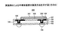
【解決手段】支持基板上に第1のソルダーレジスト層102を形成し、第1のソルダーレジスト層102に第1の開口部を形成し、第1の開口部に電極を103形成する。電極103上に絶縁層104を形成し、絶縁層104に電極103に接続される配線部106を形成する。配線部106上に第2のソルダーレジスト層107を形成し、第2のソルダーレジスト層107に第2の開口部107Aを形成する。支持基板を除去し、配線基板を得る。
【選択図】図1E
Description
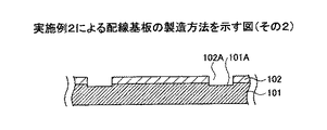
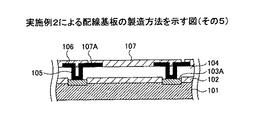
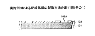
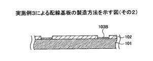
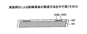
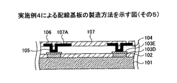
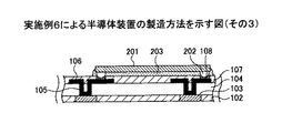
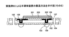
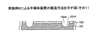
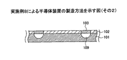
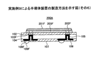
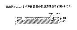
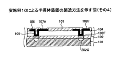
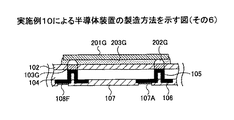
101,101a 支持基板
102,107,107a ソルダーレジスト層
103,103a,103A,103C,103E 電極
104,104a 絶縁層
105,105a ビアプラグ
106,106a パターン配線
102A,107A 開口部
201,201F,201G 半導体チップ
202F,202G 半田ボール
203F,203G アンダーフィル
Claims (13)
- 支持基板上に第1の開口部を有する第1のソルダーレジスト層を形成する第1の工程と、
前記第1の開口部に電極を形成する第2の工程と、
前記電極上に絶縁層を形成し、当該絶縁層に前記電極に接続される配線部を形成する第3の工程と、
当該配線部上に第2の開口部を有する第2のソルダーレジスト層を形成する第4の工程と、
前記支持基板を除去する第5の工程と、を有することを特徴とする配線基板の製造方法。 - 前記支持基板は導電性材料よりなり、前記電極は電解メッキ法により形成されることを特徴とする請求項1記載の配線基板の製造方法。
- 前記第2の工程は、前記支持基板をエッチングして凹部を形成する工程を含み、前記電極は前記凹部に対応するように形成されることを特徴とする請求項1または2記載の配線基板の製造方法。
- 前記第2の工程は、前記第1の開口部に電極高さ調整層を形成する工程を含み、前記電極は前記電極高さ調整層上に形成されることを特徴とする請求項1または2記載の配線基板の製造方法。
- 前記第5の工程では前記支持基板と共に前記電極高さ調整層が除去されることを特徴とする請求項4記載の配線基板の製造方法。
- 前記支持基板および前記高さ調整層はCuまたはCu合金よりなることを特徴とする請求項4または5記載の配線基板の製造方法。
- 前記電極高さ調整層の厚さが前記第1のソルダーレジスト層の厚さ以上であることを特徴とする請求項4乃至6のうち、いずれか1項記載の配線基板の製造方法。
- 前記電極の面積が前記第1の開口部の面積より大きいことを特徴とする請求項7記載の配線基板の製造方法。
- 前記支持基板は別の支持基板と貼り合わせられており、
前記別の支持基板に第3の開口部を有する第3のソルダーレジスト層を形成する第6の工程と、
前記第3の開口部に別の電極を形成する第7の工程と、
前記別の電極を覆うように別の絶縁層を形成し、当該別の絶縁層に、前記別の電極に接続される別の配線部を形成する第8の工程と、
前記別の配線部を覆うように第4の開口部を有する第4のソルダーレジスト層を形成する第9の工程と、
前記別の支持基板を除去する第10の工程と、をさらに有することを特徴とする請求項1乃至8のうち、いずれか1項記載の配線基板の製造方法。 - 請求項1乃至9のうち、いずれか1項記載の配線基板の製造方法を用いた半導体装置の製造方法であって、
前記第4の工程の後に、前記第2の開口部から前記配線部に電気的に接続されるように半導体チップを実装する実装工程をさらに有することを特徴とする半導体装置の製造方法。 - 前記第1の工程の後に、前記第1の開口部から露出する前記支持基板をエッチングするとともに、エッチングされた該支持基板に外部接続端子を形成する工程をさらに有することを特徴とする請求項10記載の半導体装置の製造方法。
- 請求項1乃至9のうち、いずれか1項記載の配線基板の製造方法を用いた半導体装置の製造方法であって、
前記第5の工程の後に、前記電極を介して前記配線部に電気的に接続されるように半導体チップを実装する実装工程をさらに有することを特徴とする半導体装置の製造方法。 - 前記第1の工程の後に、前記第1の開口部から露出する前記支持基板をエッチングするとともに、エッチングされた該支持基板に半導体チップ接続端子を形成する工程をさらに有し、前記半導体チップは前記半導体チップ接続端子上に実装されることを特徴とする請求項12記載の半導体装置の製造方法。
Priority Applications (8)
| Application Number | Priority Date | Filing Date | Title |
|---|---|---|---|
| JP2006014199A JP4146864B2 (ja) | 2005-05-31 | 2006-01-23 | 配線基板及びその製造方法、並びに半導体装置及び半導体装置の製造方法 |
| US11/419,887 US8015700B2 (en) | 2005-05-31 | 2006-05-23 | Method of fabricating wiring board and method of fabricating semiconductor device |
| KR1020060046012A KR20060124576A (ko) | 2005-05-31 | 2006-05-23 | 배선 기판의 제조 방법 및 반도체 장치의 제조 방법 |
| TW095118980A TWI437668B (zh) | 2005-05-31 | 2006-05-29 | 佈線板、半導體裝置、佈線板之製造方法及半導體裝置之製造方法 |
| CN2006100836413A CN1873935B (zh) | 2005-05-31 | 2006-05-31 | 配线基板的制造方法及半导体器件的制造方法 |
| US13/196,129 US8455770B2 (en) | 2005-05-31 | 2011-08-02 | Method of fabricating wiring board and method of fabricating semiconductor device |
| KR1020120088942A KR101344800B1 (ko) | 2005-05-31 | 2012-08-14 | 배선 기판 및 반도체 장치 |
| US13/873,504 US9155195B2 (en) | 2005-05-31 | 2013-04-30 | Wiring board and semiconductor device |
Applications Claiming Priority (2)
| Application Number | Priority Date | Filing Date | Title |
|---|---|---|---|
| JP2005159993 | 2005-05-31 | ||
| JP2006014199A JP4146864B2 (ja) | 2005-05-31 | 2006-01-23 | 配線基板及びその製造方法、並びに半導体装置及び半導体装置の製造方法 |
Related Child Applications (1)
| Application Number | Title | Priority Date | Filing Date |
|---|---|---|---|
| JP2008133992A Division JP4980295B2 (ja) | 2005-05-31 | 2008-05-22 | 配線基板の製造方法、及び半導体装置の製造方法 |
Publications (3)
| Publication Number | Publication Date |
|---|---|
| JP2007013092A true JP2007013092A (ja) | 2007-01-18 |
| JP2007013092A5 JP2007013092A5 (ja) | 2008-01-17 |
| JP4146864B2 JP4146864B2 (ja) | 2008-09-10 |
Family
ID=37464013
Family Applications (1)
| Application Number | Title | Priority Date | Filing Date |
|---|---|---|---|
| JP2006014199A Expired - Fee Related JP4146864B2 (ja) | 2005-05-31 | 2006-01-23 | 配線基板及びその製造方法、並びに半導体装置及び半導体装置の製造方法 |
Country Status (4)
| Country | Link |
|---|---|
| US (3) | US8015700B2 (ja) |
| JP (1) | JP4146864B2 (ja) |
| KR (2) | KR20060124576A (ja) |
| TW (1) | TWI437668B (ja) |
Cited By (14)
| Publication number | Priority date | Publication date | Assignee | Title |
|---|---|---|---|---|
| JP2008270346A (ja) * | 2007-04-17 | 2008-11-06 | Shinko Electric Ind Co Ltd | 配線基板の製造方法及び半導体装置の製造方法及び配線基板 |
| KR20100133317A (ko) | 2009-06-11 | 2010-12-21 | 신코 덴키 코교 가부시키가이샤 | 배선기판의 제조방법 |
| JP2012069972A (ja) * | 2011-11-04 | 2012-04-05 | Shinko Electric Ind Co Ltd | 配線基板の製造方法及び半導体パッケージの製造方法 |
| JP2012124363A (ja) * | 2010-12-09 | 2012-06-28 | Ngk Spark Plug Co Ltd | 多層配線基板の製造方法 |
| JP2013009006A (ja) * | 2012-09-26 | 2013-01-10 | Shinko Electric Ind Co Ltd | 配線基板とその製造方法 |
| US8476754B2 (en) | 2009-06-03 | 2013-07-02 | Shinko Electric Industries Co., Ltd. | Wiring substrate and method of manufacturing the same |
| US8502398B2 (en) | 2007-10-05 | 2013-08-06 | Shinko Electric Industries Co., Ltd. | Wiring board, semiconductor apparatus and method of manufacturing them |
| US8610287B2 (en) | 2009-12-21 | 2013-12-17 | Shinko Electric Industries Co., Ltd. | Wiring substrate and method of manufacturing the same |
| JP2015073068A (ja) * | 2013-10-01 | 2015-04-16 | 旭徳科技股▲ふん▼有限公司 | パッケージキャリア |
| US9258899B2 (en) | 2007-05-30 | 2016-02-09 | Shinko Electric Industries Co., Ltd. | Method of fabricating a wiring board |
| JP2017163058A (ja) * | 2016-03-10 | 2017-09-14 | パナソニックIpマネジメント株式会社 | Ledモジュール |
| JP2017163053A (ja) * | 2016-03-10 | 2017-09-14 | パナソニックIpマネジメント株式会社 | Ledモジュール |
| JP2021034573A (ja) * | 2019-08-26 | 2021-03-01 | ローム株式会社 | 半導体装置 |
| KR20230038559A (ko) * | 2020-07-15 | 2023-03-20 | 주하이 엑세스 세미컨덕터 컴퍼니., 리미티드 | 패키지 기판 제작 방법 |
Families Citing this family (15)
| Publication number | Priority date | Publication date | Assignee | Title |
|---|---|---|---|---|
| JP5557439B2 (ja) * | 2008-10-24 | 2014-07-23 | ピーエスフォー ルクスコ エスエイアールエル | 半導体装置及びその製造方法 |
| US8569894B2 (en) | 2010-01-13 | 2013-10-29 | Advanced Semiconductor Engineering, Inc. | Semiconductor package with single sided substrate design and manufacturing methods thereof |
| JP5623308B2 (ja) | 2010-02-26 | 2014-11-12 | 日本特殊陶業株式会社 | 多層配線基板及びその製造方法 |
| TWI411075B (zh) | 2010-03-22 | 2013-10-01 | 日月光半導體製造股份有限公司 | 半導體封裝件及其製造方法 |
| JP5638269B2 (ja) | 2010-03-26 | 2014-12-10 | 日本特殊陶業株式会社 | 多層配線基板 |
| JP5566771B2 (ja) | 2010-05-18 | 2014-08-06 | 日本特殊陶業株式会社 | 多層配線基板 |
| JP5502624B2 (ja) * | 2010-07-08 | 2014-05-28 | 新光電気工業株式会社 | 配線基板の製造方法及び配線基板 |
| US9406658B2 (en) | 2010-12-17 | 2016-08-02 | Advanced Semiconductor Engineering, Inc. | Embedded component device and manufacturing methods thereof |
| JP5795225B2 (ja) * | 2011-09-27 | 2015-10-14 | 新光電気工業株式会社 | 配線基板の製造方法 |
| US8698008B2 (en) | 2011-12-12 | 2014-04-15 | Advance Materials Corporation | Packaging substrate and fabrication method thereof |
| KR20150064445A (ko) * | 2013-12-03 | 2015-06-11 | 삼성전기주식회사 | 반도체 패키지용 코어리스 기판 및 그 제조 방법, 이를 이용한 반도체 패키지 제조 방법 |
| JP2015231003A (ja) * | 2014-06-06 | 2015-12-21 | イビデン株式会社 | 回路基板および回路基板の製造方法 |
| CN105407651B (zh) * | 2014-09-12 | 2018-06-26 | 深南电路有限公司 | 一种电路板上设置阻焊层的方法 |
| KR102231100B1 (ko) * | 2014-10-02 | 2021-03-23 | 삼성전기주식회사 | 인쇄회로기판 및 그 제조 방법 |
| KR20230096382A (ko) * | 2021-12-23 | 2023-06-30 | 삼성전기주식회사 | 인쇄회로기판 제조 방법 |
Family Cites Families (33)
| Publication number | Priority date | Publication date | Assignee | Title |
|---|---|---|---|---|
| US4889584A (en) * | 1989-03-31 | 1989-12-26 | Meiko Electronics Co., Ltd. | Method of producing conductor circuit boards |
| JPH04322252A (ja) | 1991-04-23 | 1992-11-12 | Hitachi Ltd | 光硬化性レジスト組成物の調整方法 |
| US5886877A (en) * | 1995-10-13 | 1999-03-23 | Meiko Electronics Co., Ltd. | Circuit board, manufacturing method therefor, and bump-type contact head and semiconductor component packaging module using the circuit board |
| EP1921902B1 (en) * | 1996-12-19 | 2011-03-02 | Ibiden Co., Ltd. | Multilayered printed circuit board |
| JPH11307883A (ja) | 1998-04-20 | 1999-11-05 | Ngk Spark Plug Co Ltd | 配線基板 |
| JP3437453B2 (ja) | 1998-07-06 | 2003-08-18 | イビデン株式会社 | Icチップ実装用プリント配線板およびその製造方法 |
| US6915566B2 (en) * | 1999-03-01 | 2005-07-12 | Texas Instruments Incorporated | Method of fabricating flexible circuits for integrated circuit interconnections |
| JP3949849B2 (ja) * | 1999-07-19 | 2007-07-25 | 日東電工株式会社 | チップサイズパッケージ用インターポーザーの製造方法およびチップサイズパッケージ用インターポーザー |
| US6210992B1 (en) * | 1999-08-31 | 2001-04-03 | Micron Technology, Inc. | Controlling packaging encapsulant leakage |
| JP2001094259A (ja) | 1999-09-24 | 2001-04-06 | Jsr Corp | 多層配線板およびその製造方法 |
| EP1990832A3 (en) * | 2000-02-25 | 2010-09-29 | Ibiden Co., Ltd. | Multilayer printed circuit board and multilayer printed circuit board manufacturing method |
| JP3677429B2 (ja) * | 2000-03-09 | 2005-08-03 | Necエレクトロニクス株式会社 | フリップチップ型半導体装置の製造方法 |
| JP3546961B2 (ja) | 2000-10-18 | 2004-07-28 | 日本電気株式会社 | 半導体装置搭載用配線基板およびその製造方法、並びに半導体パッケージ |
| JP2002261190A (ja) | 2001-02-28 | 2002-09-13 | Sony Corp | 半導体装置、その製造方法及び電子機器 |
| EP1280204A3 (en) * | 2001-06-27 | 2004-09-01 | Shinko Electric Industries Co. Ltd. | Wiring substrate having position problem |
| JP3910387B2 (ja) * | 2001-08-24 | 2007-04-25 | 新光電気工業株式会社 | 半導体パッケージ及びその製造方法並びに半導体装置 |
| KR100516795B1 (ko) * | 2001-10-31 | 2005-09-26 | 신꼬오덴기 고교 가부시키가이샤 | 반도체 장치용 다층 회로 기판의 제조 방법 |
| JP3666591B2 (ja) * | 2002-02-01 | 2005-06-29 | 株式会社トッパンNecサーキットソリューションズ | 半導体チップ搭載用基板の製造方法 |
| US7474538B2 (en) * | 2002-05-27 | 2009-01-06 | Nec Corporation | Semiconductor device mounting board, method of manufacturing the same, method of inspecting the same, and semiconductor package |
| JP2004066017A (ja) * | 2002-08-01 | 2004-03-04 | Nippon Paint Co Ltd | ソルダーレジスト膜の形成方法 |
| JP3990962B2 (ja) * | 2002-09-17 | 2007-10-17 | 新光電気工業株式会社 | 配線基板の製造方法 |
| KR100499006B1 (ko) * | 2002-12-30 | 2005-07-01 | 삼성전기주식회사 | 도금 인입선이 없는 패키지 기판의 제조 방법 |
| WO2004081376A1 (ja) | 2003-03-12 | 2004-09-23 | Yasuhiro Fujita | 太陽光発電と風力発電を複合した発電装置 |
| TWI326910B (en) | 2003-03-31 | 2010-07-01 | Sanyo Electric Co | Semiconductor module and method for making same |
| JP4067507B2 (ja) | 2003-03-31 | 2008-03-26 | 三洋電機株式会社 | 半導体モジュールおよびその製造方法 |
| US20060289203A1 (en) * | 2003-05-19 | 2006-12-28 | Dai Nippon Printing Co., Ltd. | Double-sided wiring board, double sided wiring board manufacturing method, and multilayer wiring board |
| JP2005129904A (ja) | 2003-09-29 | 2005-05-19 | Sanyo Electric Co Ltd | 半導体装置およびその製造方法 |
| JP4271590B2 (ja) * | 2004-01-20 | 2009-06-03 | 新光電気工業株式会社 | 半導体装置及びその製造方法 |
| US7468645B2 (en) * | 2004-01-29 | 2008-12-23 | Sanyo Electric Co., Ltd. | Signal line circuit device |
| TWI255535B (en) * | 2004-03-31 | 2006-05-21 | Sanyo Electric Co | Device mounting board and semiconductor apparatus using the same |
| JP4361826B2 (ja) * | 2004-04-20 | 2009-11-11 | 新光電気工業株式会社 | 半導体装置 |
| JP4333492B2 (ja) | 2004-06-16 | 2009-09-16 | ソニー株式会社 | 回路モジュール体の製造方法 |
| US7361979B2 (en) * | 2004-12-29 | 2008-04-22 | Tessera, Inc. | Multi-sheet conductive substrates for microelectronic devices and methods for forming such substrates |
-
2006
- 2006-01-23 JP JP2006014199A patent/JP4146864B2/ja not_active Expired - Fee Related
- 2006-05-23 US US11/419,887 patent/US8015700B2/en active Active
- 2006-05-23 KR KR1020060046012A patent/KR20060124576A/ko not_active Ceased
- 2006-05-29 TW TW095118980A patent/TWI437668B/zh not_active IP Right Cessation
-
2011
- 2011-08-02 US US13/196,129 patent/US8455770B2/en not_active Expired - Fee Related
-
2012
- 2012-08-14 KR KR1020120088942A patent/KR101344800B1/ko not_active Expired - Fee Related
-
2013
- 2013-04-30 US US13/873,504 patent/US9155195B2/en active Active
Cited By (25)
| Publication number | Priority date | Publication date | Assignee | Title |
|---|---|---|---|---|
| JP2008270346A (ja) * | 2007-04-17 | 2008-11-06 | Shinko Electric Ind Co Ltd | 配線基板の製造方法及び半導体装置の製造方法及び配線基板 |
| US8225502B2 (en) | 2007-04-17 | 2012-07-24 | Shinko Electric Industries Co., Ltd. | Wiring board manufacturing method |
| US9258899B2 (en) | 2007-05-30 | 2016-02-09 | Shinko Electric Industries Co., Ltd. | Method of fabricating a wiring board |
| TWI447874B (zh) * | 2007-10-05 | 2014-08-01 | 新光電氣工業股份有限公司 | 佈線板,半導體裝置及其等製造方法 |
| US8779602B2 (en) | 2007-10-05 | 2014-07-15 | Shinko Electric Industries Co., Ltd. | Wiring board, semiconductor apparatus and method of manufacturing them |
| US8502398B2 (en) | 2007-10-05 | 2013-08-06 | Shinko Electric Industries Co., Ltd. | Wiring board, semiconductor apparatus and method of manufacturing them |
| US8749046B2 (en) | 2009-06-03 | 2014-06-10 | Shinko Electric Industries Co., Ltd. | Wiring substrate and method of manufacturing the same |
| US8476754B2 (en) | 2009-06-03 | 2013-07-02 | Shinko Electric Industries Co., Ltd. | Wiring substrate and method of manufacturing the same |
| US8790504B2 (en) | 2009-06-11 | 2014-07-29 | Shinko Electric Industries Co., Ltd. | Method of manufacturing wiring substrate |
| KR20100133317A (ko) | 2009-06-11 | 2010-12-21 | 신코 덴키 코교 가부시키가이샤 | 배선기판의 제조방법 |
| US8610287B2 (en) | 2009-12-21 | 2013-12-17 | Shinko Electric Industries Co., Ltd. | Wiring substrate and method of manufacturing the same |
| US8535546B2 (en) | 2010-12-09 | 2013-09-17 | Ngk Spark Plug Co., Ltd. | Method of manufacturing multilayer wiring substrate |
| JP2012124363A (ja) * | 2010-12-09 | 2012-06-28 | Ngk Spark Plug Co Ltd | 多層配線基板の製造方法 |
| JP2012069972A (ja) * | 2011-11-04 | 2012-04-05 | Shinko Electric Ind Co Ltd | 配線基板の製造方法及び半導体パッケージの製造方法 |
| JP2013009006A (ja) * | 2012-09-26 | 2013-01-10 | Shinko Electric Ind Co Ltd | 配線基板とその製造方法 |
| JP2015073068A (ja) * | 2013-10-01 | 2015-04-16 | 旭徳科技股▲ふん▼有限公司 | パッケージキャリア |
| US9433099B2 (en) | 2013-10-01 | 2016-08-30 | Subtron Technology Co., Ltd. | Package carrier |
| JP2017163058A (ja) * | 2016-03-10 | 2017-09-14 | パナソニックIpマネジメント株式会社 | Ledモジュール |
| JP2017163053A (ja) * | 2016-03-10 | 2017-09-14 | パナソニックIpマネジメント株式会社 | Ledモジュール |
| JP2021034573A (ja) * | 2019-08-26 | 2021-03-01 | ローム株式会社 | 半導体装置 |
| JP7382175B2 (ja) | 2019-08-26 | 2023-11-16 | ローム株式会社 | 半導体装置 |
| KR20230038559A (ko) * | 2020-07-15 | 2023-03-20 | 주하이 엑세스 세미컨덕터 컴퍼니., 리미티드 | 패키지 기판 제작 방법 |
| JP2023534256A (ja) * | 2020-07-15 | 2023-08-08 | 珠海越亜半導体股▲分▼有限公司 | パッケージ基板の製作方法 |
| JP7534523B2 (ja) | 2020-07-15 | 2024-08-14 | 珠海越亜半導体股▲分▼有限公司 | パッケージ基板の製作方法 |
| KR102786330B1 (ko) * | 2020-07-15 | 2025-03-24 | 주하이 엑세스 세미컨덕터 컴퍼니., 리미티드 | 패키지 기판 제작 방법 |
Also Published As
| Publication number | Publication date |
|---|---|
| KR20060124576A (ko) | 2006-12-05 |
| KR20120109427A (ko) | 2012-10-08 |
| US20130235543A1 (en) | 2013-09-12 |
| US9155195B2 (en) | 2015-10-06 |
| US8455770B2 (en) | 2013-06-04 |
| KR101344800B1 (ko) | 2013-12-26 |
| US8015700B2 (en) | 2011-09-13 |
| JP4146864B2 (ja) | 2008-09-10 |
| US20110286189A1 (en) | 2011-11-24 |
| TW200703590A (en) | 2007-01-16 |
| TWI437668B (zh) | 2014-05-11 |
| US20060270211A1 (en) | 2006-11-30 |
Similar Documents
| Publication | Publication Date | Title |
|---|---|---|
| JP4146864B2 (ja) | 配線基板及びその製造方法、並びに半導体装置及び半導体装置の製造方法 | |
| JP4980295B2 (ja) | 配線基板の製造方法、及び半導体装置の製造方法 | |
| JP5101451B2 (ja) | 配線基板及びその製造方法 | |
| CN100435299C (zh) | 布线基板的制备方法 | |
| JP5101169B2 (ja) | 配線基板とその製造方法 | |
| TWI443791B (zh) | 佈線基板之製造方法、半導體裝置之製造方法及佈線基板 | |
| TWI557855B (zh) | 封裝載板及其製作方法 | |
| US9711476B2 (en) | Wiring board and electronic component device | |
| CN101409238A (zh) | 无核层封装基板的制作方法 | |
| JP2008060573A (ja) | 電子素子内蔵型印刷回路基板の製造方法 | |
| JP2018032657A (ja) | プリント配線板およびプリント配線板の製造方法 | |
| TW201424497A (zh) | 電路板及其製作方法 | |
| US8061024B2 (en) | Method of fabricating a circuit board and semiconductor package. | |
| JP2005243850A (ja) | 多層プリント配線基板及びその製造方法 | |
| CN1791311B (zh) | 制造电路基板的方法和制造电子部件封装结构的方法 | |
| JP2009147080A (ja) | 半導体装置用パッケージおよびその製造方法 | |
| US20250113438A1 (en) | Wiring board and semiconductor device | |
| TWI461134B (zh) | 載板結構及其製作方法 | |
| TWI496243B (zh) | 元件內埋式半導體封裝件的製作方法 | |
| JP5511922B2 (ja) | 配線基板とその製造方法 | |
| JP4591098B2 (ja) | 半導体素子搭載用基板の製造方法 | |
| JP2005093930A (ja) | 多層基板とその製造方法 | |
| JP2013084812A (ja) | 半導体パッケージの製造方法及び半導体パッケージ |
Legal Events
| Date | Code | Title | Description |
|---|---|---|---|
| A521 | Request for written amendment filed |
Free format text: JAPANESE INTERMEDIATE CODE: A523 Effective date: 20071127 |
|
| A621 | Written request for application examination |
Free format text: JAPANESE INTERMEDIATE CODE: A621 Effective date: 20071127 |
|
| A871 | Explanation of circumstances concerning accelerated examination |
Free format text: JAPANESE INTERMEDIATE CODE: A871 Effective date: 20071127 |
|
| A131 | Notification of reasons for refusal |
Free format text: JAPANESE INTERMEDIATE CODE: A131 Effective date: 20080108 |
|
| A975 | Report on accelerated examination |
Free format text: JAPANESE INTERMEDIATE CODE: A971005 Effective date: 20080325 |
|
| A131 | Notification of reasons for refusal |
Free format text: JAPANESE INTERMEDIATE CODE: A131 Effective date: 20080401 |
|
| A521 | Request for written amendment filed |
Free format text: JAPANESE INTERMEDIATE CODE: A523 Effective date: 20080522 |
|
| TRDD | Decision of grant or rejection written | ||
| A01 | Written decision to grant a patent or to grant a registration (utility model) |
Free format text: JAPANESE INTERMEDIATE CODE: A01 Effective date: 20080617 |
|
| A01 | Written decision to grant a patent or to grant a registration (utility model) |
Free format text: JAPANESE INTERMEDIATE CODE: A01 |
|
| A61 | First payment of annual fees (during grant procedure) |
Free format text: JAPANESE INTERMEDIATE CODE: A61 Effective date: 20080620 |
|
| R150 | Certificate of patent or registration of utility model |
Free format text: JAPANESE INTERMEDIATE CODE: R150 Ref document number: 4146864 Country of ref document: JP Free format text: JAPANESE INTERMEDIATE CODE: R150 |
|
| FPAY | Renewal fee payment (event date is renewal date of database) |
Free format text: PAYMENT UNTIL: 20110627 Year of fee payment: 3 |
|
| FPAY | Renewal fee payment (event date is renewal date of database) |
Free format text: PAYMENT UNTIL: 20110627 Year of fee payment: 3 |
|
| FPAY | Renewal fee payment (event date is renewal date of database) |
Free format text: PAYMENT UNTIL: 20120627 Year of fee payment: 4 |
|
| FPAY | Renewal fee payment (event date is renewal date of database) |
Free format text: PAYMENT UNTIL: 20120627 Year of fee payment: 4 |
|
| FPAY | Renewal fee payment (event date is renewal date of database) |
Free format text: PAYMENT UNTIL: 20130627 Year of fee payment: 5 |
|
| LAPS | Cancellation because of no payment of annual fees |