JP2007019049A - チップマウント用配線シート、シートマウントチップおよびシートマウントチップの製造方法 - Google Patents
チップマウント用配線シート、シートマウントチップおよびシートマウントチップの製造方法 Download PDFInfo
- Publication number
- JP2007019049A JP2007019049A JP2003364389A JP2003364389A JP2007019049A JP 2007019049 A JP2007019049 A JP 2007019049A JP 2003364389 A JP2003364389 A JP 2003364389A JP 2003364389 A JP2003364389 A JP 2003364389A JP 2007019049 A JP2007019049 A JP 2007019049A
- Authority
- JP
- Japan
- Prior art keywords
- chip
- sheet
- terminal
- test
- semiconductor chip
- Prior art date
- Legal status (The legal status is an assumption and is not a legal conclusion. Google has not performed a legal analysis and makes no representation as to the accuracy of the status listed.)
- Pending
Links
Images



Classifications
-
- H—ELECTRICITY
- H10—SEMICONDUCTOR DEVICES; ELECTRIC SOLID-STATE DEVICES NOT OTHERWISE PROVIDED FOR
- H10P—GENERIC PROCESSES OR APPARATUS FOR THE MANUFACTURE OR TREATMENT OF DEVICES COVERED BY CLASS H10
- H10P74/00—Testing or measuring during manufacture or treatment of wafers, substrates or devices
- H10P74/27—Structural arrangements therefor
- H10P74/273—Interconnections for measuring or testing, e.g. probe pads
-
- G—PHYSICS
- G01—MEASURING; TESTING
- G01R—MEASURING ELECTRIC VARIABLES; MEASURING MAGNETIC VARIABLES
- G01R31/00—Arrangements for testing electric properties; Arrangements for locating electric faults; Arrangements for electrical testing characterised by what is being tested not provided for elsewhere
- G01R31/28—Testing of electronic circuits, e.g. by signal tracer
- G01R31/2851—Testing of integrated circuits [IC]
- G01R31/2884—Testing of integrated circuits [IC] using dedicated test connectors, test elements or test circuits on the IC under test
-
- H—ELECTRICITY
- H10—SEMICONDUCTOR DEVICES; ELECTRIC SOLID-STATE DEVICES NOT OTHERWISE PROVIDED FOR
- H10W—GENERIC PACKAGES, INTERCONNECTIONS, CONNECTORS OR OTHER CONSTRUCTIONAL DETAILS OF DEVICES COVERED BY CLASS H10
- H10W70/00—Package substrates; Interposers; Redistribution layers [RDL]
- H10W70/60—Insulating or insulated package substrates; Interposers; Redistribution layers
- H10W70/611—Insulating or insulated package substrates; Interposers; Redistribution layers for connecting multiple chips together
-
- H—ELECTRICITY
- H10—SEMICONDUCTOR DEVICES; ELECTRIC SOLID-STATE DEVICES NOT OTHERWISE PROVIDED FOR
- H10W—GENERIC PACKAGES, INTERCONNECTIONS, CONNECTORS OR OTHER CONSTRUCTIONAL DETAILS OF DEVICES COVERED BY CLASS H10
- H10W70/00—Package substrates; Interposers; Redistribution layers [RDL]
- H10W70/60—Insulating or insulated package substrates; Interposers; Redistribution layers
- H10W70/62—Insulating or insulated package substrates; Interposers; Redistribution layers characterised by their interconnections
- H10W70/65—Shapes or dispositions of interconnections
-
- G—PHYSICS
- G01—MEASURING; TESTING
- G01R—MEASURING ELECTRIC VARIABLES; MEASURING MAGNETIC VARIABLES
- G01R31/00—Arrangements for testing electric properties; Arrangements for locating electric faults; Arrangements for electrical testing characterised by what is being tested not provided for elsewhere
- G01R31/28—Testing of electronic circuits, e.g. by signal tracer
- G01R31/2851—Testing of integrated circuits [IC]
- G01R31/2855—Environmental, reliability or burn-in testing
- G01R31/286—External aspects, e.g. related to chambers, contacting devices or handlers
- G01R31/2863—Contacting devices, e.g. sockets, burn-in boards or mounting fixtures
-
- H—ELECTRICITY
- H10—SEMICONDUCTOR DEVICES; ELECTRIC SOLID-STATE DEVICES NOT OTHERWISE PROVIDED FOR
- H10W—GENERIC PACKAGES, INTERCONNECTIONS, CONNECTORS OR OTHER CONSTRUCTIONAL DETAILS OF DEVICES COVERED BY CLASS H10
- H10W72/00—Interconnections or connectors in packages
- H10W72/90—Bond pads, in general
- H10W72/931—Shapes of bond pads
- H10W72/932—Plan-view shape, i.e. in top view
-
- H—ELECTRICITY
- H10—SEMICONDUCTOR DEVICES; ELECTRIC SOLID-STATE DEVICES NOT OTHERWISE PROVIDED FOR
- H10W—GENERIC PACKAGES, INTERCONNECTIONS, CONNECTORS OR OTHER CONSTRUCTIONAL DETAILS OF DEVICES COVERED BY CLASS H10
- H10W90/00—Package configurations
- H10W90/20—Configurations of stacked chips
- H10W90/24—Configurations of stacked chips at least one of the stacked chips being laterally offset from a neighbouring stacked chip, e.g. chip stacks having a staircase shape
-
- H—ELECTRICITY
- H10—SEMICONDUCTOR DEVICES; ELECTRIC SOLID-STATE DEVICES NOT OTHERWISE PROVIDED FOR
- H10W—GENERIC PACKAGES, INTERCONNECTIONS, CONNECTORS OR OTHER CONSTRUCTIONAL DETAILS OF DEVICES COVERED BY CLASS H10
- H10W90/00—Package configurations
- H10W90/701—Package configurations characterised by the relative positions of pads or connectors relative to package parts
- H10W90/751—Package configurations characterised by the relative positions of pads or connectors relative to package parts of bond wires
- H10W90/752—Package configurations characterised by the relative positions of pads or connectors relative to package parts of bond wires between stacked chips
-
- H—ELECTRICITY
- H10—SEMICONDUCTOR DEVICES; ELECTRIC SOLID-STATE DEVICES NOT OTHERWISE PROVIDED FOR
- H10W—GENERIC PACKAGES, INTERCONNECTIONS, CONNECTORS OR OTHER CONSTRUCTIONAL DETAILS OF DEVICES COVERED BY CLASS H10
- H10W90/00—Package configurations
- H10W90/701—Package configurations characterised by the relative positions of pads or connectors relative to package parts
- H10W90/751—Package configurations characterised by the relative positions of pads or connectors relative to package parts of bond wires
- H10W90/754—Package configurations characterised by the relative positions of pads or connectors relative to package parts of bond wires between a chip and a stacked insulating package substrate, interposer or RDL
Landscapes
- Engineering & Computer Science (AREA)
- Computer Hardware Design (AREA)
- Microelectronics & Electronic Packaging (AREA)
- General Engineering & Computer Science (AREA)
- Physics & Mathematics (AREA)
- General Physics & Mathematics (AREA)
- Wire Bonding (AREA)
- Testing Of Individual Semiconductor Devices (AREA)
- Testing Or Measuring Of Semiconductors Or The Like (AREA)
Abstract
【解決手段】 複数の単位区画20′が形成されたチップマウント用配線シート200の各単位区画20′のチップマウント部100に半導体チップ50をマウントする。このシートのままの状態で、テスト用端子25にテスト装置を接続して各半導体チップ50の各種テストを行う。このテストには、チップ状態では行えない高温バイアス試験(Burn-in)なども含まれる。このテストののち、テスト用端子25を含まない配線シート部20の領域のみ切り離すことにより、KGDとしてのシートマウントチップ60を得ることができる。
【選択図】 図1
Description
日経エレクトロニクス2002,2-11 no.815 p108 「第1部 チップがダメならパッケージがある」
また、この発明によれば、完全にチップサイズのシートマウントチップを製造することができる。
なお、この場合でも、テスト信号線に多重化したテスト信号を入力することにより、複数の半導体チップに対してそれぞれ独立したテストを行うことが可能である。
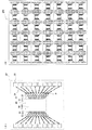
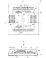
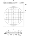
10−パッケージ基板
11−端子
12−半田ボール
13−封止樹脂
20−配線シート部
20′−単位区画
21−内部端子、
22−外部端子
23,24−内部配線
25−テスト用端子
30,40,50−半導体チップ
31,41,51−端子
60−シートマウントチップ
70−(半導体チップ50が形成された)ウェハ
100−チップマウントエリア
200−チップマウント用配線シート
W−ワイヤ
Claims (10)
- 複数の半導体チップをマウントする配線シートであって、
チップマウント部にマウントされた半導体チップに接続される内部端子と、
実装時に他の部品に接続される外部端子と、
試験時に試験装置の端子が接続されるテスト用端子と、
前記内部端子と前記外部端子およびテスト用端子とを電気的に接続する内部配線と、
を各半導体チップ毎に備えたことを特徴とするチップマウント用配線シート。 - 前記テスト用端子は、前記外部端子よりもチップマウント部に対して外側に形成されている請求項1に記載のチップマウント用配線シート。
- 前記テスト用端子は、シートの端部に形成されている請求項1に記載のチップマウント用配線シート。
- 前記テスト用端子は、複数の半導体チップで共通である請求項3に記載のチップマウント用配線シート。
- 半導体チップがマウントされた請求項1乃至請求項4のいずれかに記載のチップマウント用配線シートを、各半導体チップ毎に、チップマウント部、内部端子および外部端子を含み、テスト用端子の少なくとも一部を含まない形状に切り抜いて形成したことを特徴とするシートマウントチップ。
- 請求項1乃至請求項4のいずれかに記載のチップマウント用配線シートに半導体チップをマウントする手順、
テスト用端子に試験装置の端子を接続して各半導体チップの試験を行う手順、
各半導体チップ毎に、チップマウント部、内部端子および外部端子を含み、テスト用端子を含まない形状に切り抜く手順、
を有することを特徴とするシートマウントチップの製造方法。 - 複数の半導体チップが形成されたウェハに貼り付けられる配線シートであって、
各半導体チップのパッドに対向して電気的に接続される内部端子と、
貼付面の裏面に形成され、実装時に他の部品に接続される外部端子と、
前記ウェハの貼り付け範囲外または貼付面の裏面に形成され、試験時に試験装置の端子が接続されるテスト用端子と、
前記内部端子と前記外部端子およびテスト用端子とを電気的に接続する内部配線と、
を備えたことを特徴とするチップマウント用配線シート。 - 前記テスト用端子は、シートの端部に形成され、複数の半導体チップで共通である請求項7に記載のチップマウント用配線シート。
- 請求項7または請求項8に記載のチップマウント用配線シートに貼り付けた半導体チップが形成されたウェハを、各半導体チップ毎にカットして形成したことを特徴とするシートマウントチップ。
- 請求項7または請求項8に記載のチップマウント用配線シートに半導体チップが形成されたウェハを貼り付ける手順、
テスト用端子に試験装置の端子を接続して各半導体チップの試験を行う手順、
前記ウェハおよびチップマウント用配線シートを各半導体チップ毎にカットする手順、
を有することを特徴とするシートマウントチップの製造方法。
Priority Applications (2)
| Application Number | Priority Date | Filing Date | Title |
|---|---|---|---|
| JP2003364389A JP2007019049A (ja) | 2003-10-24 | 2003-10-24 | チップマウント用配線シート、シートマウントチップおよびシートマウントチップの製造方法 |
| PCT/JP2004/002342 WO2005041296A1 (ja) | 2003-10-24 | 2004-02-27 | チップマウント用配線シート、シートマウントチップおよびシートマウントチップの製造方法 |
Applications Claiming Priority (1)
| Application Number | Priority Date | Filing Date | Title |
|---|---|---|---|
| JP2003364389A JP2007019049A (ja) | 2003-10-24 | 2003-10-24 | チップマウント用配線シート、シートマウントチップおよびシートマウントチップの製造方法 |
Publications (1)
| Publication Number | Publication Date |
|---|---|
| JP2007019049A true JP2007019049A (ja) | 2007-01-25 |
Family
ID=34510107
Family Applications (1)
| Application Number | Title | Priority Date | Filing Date |
|---|---|---|---|
| JP2003364389A Pending JP2007019049A (ja) | 2003-10-24 | 2003-10-24 | チップマウント用配線シート、シートマウントチップおよびシートマウントチップの製造方法 |
Country Status (2)
| Country | Link |
|---|---|
| JP (1) | JP2007019049A (ja) |
| WO (1) | WO2005041296A1 (ja) |
Family Cites Families (3)
| Publication number | Priority date | Publication date | Assignee | Title |
|---|---|---|---|---|
| US5367763A (en) * | 1993-09-30 | 1994-11-29 | Atmel Corporation | TAB testing of area array interconnected chips |
| JP3527015B2 (ja) * | 1996-06-10 | 2004-05-17 | 株式会社ルネサステクノロジ | 半導体装置及びその製造方法 |
| JP2001176940A (ja) * | 1999-12-20 | 2001-06-29 | Sharp Corp | 半導体モジュールの製造方法 |
-
2003
- 2003-10-24 JP JP2003364389A patent/JP2007019049A/ja active Pending
-
2004
- 2004-02-27 WO PCT/JP2004/002342 patent/WO2005041296A1/ja not_active Ceased
Also Published As
| Publication number | Publication date |
|---|---|
| WO2005041296A1 (ja) | 2005-05-06 |
Similar Documents
| Publication | Publication Date | Title |
|---|---|---|
| US9653427B2 (en) | Integrated circuit package with probe pad structure | |
| US8994163B2 (en) | Semiconductor assemblies, stacked semiconductor devices, and methods of manufacturing semiconductor assemblies and stacked semiconductor devices | |
| CN108140615B (zh) | 使能对用于半导体封装的硅桥的在线测试的保护环设计 | |
| US8076179B2 (en) | Fabrication method for integrated circuit chip component, multi-chip module, and their integration structure | |
| TWI433621B (zh) | 超薄多層基板之封裝方法 | |
| US20150084051A1 (en) | Electronic Device, Test Board, and Semiconductor Device Manufacturing Method | |
| KR20030014637A (ko) | 반도체 웨이퍼와 반도체장치 및 그 제조방법 | |
| US7723835B2 (en) | Semiconductor device package structure | |
| EP2645417A1 (en) | Semiconductor module | |
| TWI474444B (zh) | 超薄多層基板之封裝方法 | |
| TWI440412B (zh) | 超薄多層基板之封裝方法 | |
| WO2019011457A1 (en) | NON DESTRUCTIVE TEST OF INTEGRATED CIRCUIT CHIPS | |
| CN101499464A (zh) | 使用穿通电极制备堆叠封装的方法 | |
| US9263379B2 (en) | IC package with metal interconnect structure implemented between metal layers of die and interposer | |
| JP3842272B2 (ja) | インターポーザー、半導体チップマウントサブ基板および半導体パッケージ | |
| JP2007019049A (ja) | チップマウント用配線シート、シートマウントチップおよびシートマウントチップの製造方法 | |
| JP4388926B2 (ja) | 半導体装置のパッケージ構造 | |
| JP4303772B2 (ja) | 半導体パッケージ | |
| JP2003273313A (ja) | 半導体装置およびその製造方法 | |
| JP4388989B2 (ja) | 半導体チップマウント封止サブ基板 | |
| JP2007142128A (ja) | 半導体装置およびその製造方法 | |
| US20080121878A1 (en) | Interposer, semiconductor chip mounted sub-board, and semiconductor package | |
| WO1999026289A1 (fr) | Dispositif a semi-conducteur et son procede de production | |
| CN118738027A (zh) | 切割线结构及其半导体元件 | |
| CN103325773A (zh) | 集成电路的封装结构 |
Legal Events
| Date | Code | Title | Description |
|---|---|---|---|
| A521 | Request for written amendment filed |
Free format text: JAPANESE INTERMEDIATE CODE: A523 Effective date: 20061023 |
|
| A621 | Written request for application examination |
Free format text: JAPANESE INTERMEDIATE CODE: A621 Effective date: 20061023 |
|
| A131 | Notification of reasons for refusal |
Free format text: JAPANESE INTERMEDIATE CODE: A131 Effective date: 20090421 |
|
| A521 | Request for written amendment filed |
Free format text: JAPANESE INTERMEDIATE CODE: A523 Effective date: 20090622 |
|
| A131 | Notification of reasons for refusal |
Free format text: JAPANESE INTERMEDIATE CODE: A131 Effective date: 20090714 |
|
| A02 | Decision of refusal |
Free format text: JAPANESE INTERMEDIATE CODE: A02 Effective date: 20100119 |